EP0447729B1 - Gegen Rauschen geschützter Schwellwertdetektor - Google Patents
Gegen Rauschen geschützter Schwellwertdetektor Download PDFInfo
- Publication number
- EP0447729B1 EP0447729B1 EP90403391A EP90403391A EP0447729B1 EP 0447729 B1 EP0447729 B1 EP 0447729B1 EP 90403391 A EP90403391 A EP 90403391A EP 90403391 A EP90403391 A EP 90403391A EP 0447729 B1 EP0447729 B1 EP 0447729B1
- Authority
- EP
- European Patent Office
- Prior art keywords
- input
- inverter
- inverters
- transistors
- vbias
- Prior art date
- Legal status (The legal status is an assumption and is not a legal conclusion. Google has not performed a legal analysis and makes no representation as to the accuracy of the status listed.)
- Expired - Lifetime
Links
Images

Classifications
-
- H—ELECTRICITY
- H03—ELECTRONIC CIRCUITRY
- H03K—PULSE TECHNIQUE
- H03K5/00—Manipulating of pulses not covered by one of the other main groups of this subclass
-
- G—PHYSICS
- G01—MEASURING; TESTING
- G01R—MEASURING ELECTRIC VARIABLES; MEASURING MAGNETIC VARIABLES
- G01R19/00—Arrangements for measuring currents or voltages or for indicating presence or sign thereof
- G01R19/165—Indicating that current or voltage is either above or below a predetermined value or within or outside a predetermined range of values
- G01R19/16528—Indicating that current or voltage is either above or below a predetermined value or within or outside a predetermined range of values using digital techniques or performing arithmetic operations
Definitions
- the invention relates to integrated circuits, and more particularly to the manner of producing a threshold comparator which is immune to noise, in particular noise constituted by variations in supply voltage Vcc of the integrated circuit or variations in electrical ground potential. .
- the threshold from which the comparator switches in one direction or the other is more or less a function of the supply voltage of the comparator, or more exactly of the difference between this voltage and ground.
- the supply voltage or in the ground potential may be more or less well distributed across the integrated circuit.
- the object of the present invention is to propose a comparison circuit which does not have the drawbacks of those of the prior art.
- a noise-protected threshold comparator comprising a signal input intended to receive a signal of variable level, characterized in that it comprises at least one input capacitance connected to the signal input. , two threshold inverters each having an input connected to the capacity, these inverters having tilting thresholds close to each other, these thresholds corresponding to an input voltage value Vbias + v for one and Vbias -v 'for the other, v and v' low compared to the supply voltage Vcc of the comparator, the outputs of the inverters being connected one to a tilting input of an RS type flip-flop and the other to l re-entry of this flip-flop, so as to cause the flip-flop of the flip-flop during a change of state of one of the inverters due to the exceeding of Vbias + v by the input signal and the re-establishment during the change of state of the other inverter as a result of the return of the input signal below Vbias-v
- the voltage Vbias is a bias voltage defined by the output of a third inverter having its input looped back to its output, this output being connected to the inputs of the first two inverters, each of the three inverters comprising two transistors in series and the the geometries of the inverter transistors being chosen such that the ratio between the geometry of the first transistor and the geometry of the second for the first inverter is slightly different from the corresponding ratio for the second inverter, the corresponding ratio for the third inverter being between first two reports.
- each of the three inverters comprises an N-channel transistor in series with a P-channel transistor.
- the input of the inverter can be constituted for example by the gate of the N-channel transistor.
- the gate of the P channel transistor can be controlled by a reference voltage Vref common to all the inverters or be connected to the input of the inverter.
- the simplest circuit implementing the invention may comprise for each inverter a P-channel transistor in series with an N-channel transistor; the gates of all the transistors P (or on the contrary N) are controlled by the same reference voltage Vref; all P transistors have the same channel width / length ratio; the N transistors of the first two inverters have slightly different width-to-length ratios, and the third inverter has a width-to-length ratio between those of the first two inverters.
- an alternative embodiment consists in providing not a third inverter to establish a bias voltage Vbias, but two "third inverters" (hereinafter called third and fourth inverters) to establish two bias voltages Vbias + v and Vbias-v 'applied respectively to the input of the first inverter and the second inverter.
- third and fourth inverters there are two capacitors connected, one between the signal input and the input of the first inverter, the other between the signal input and the input of the second inverter.
- the first inverter preferably has transistors identical to those of the third; and the second has transistors identical to those of the fourth but different from the first and from the third, the third and the fourth inverter of the polarization voltages slightly different from each other.
- the conventional diagram in FIG. 1 comprises a signal input E, intended to receive a variable signal, such as an alternating periodic signal; for example, we want to count the number of times this signal exceeds a Vbias reference level.
- a threshold comparator A is used.
- the signal input E is connected to a capacitor C which is also connected to the input of the threshold comparator A.
- the input of the comparator is biased at a fixed direct voltage Vbias which defines the comparison threshold.
- the comparator output S provides a logic level 1 each time the threshold Vbias is exceeded by the input signal.
- Vbias may also change; and this can happen when the input signal is very close to the Vbias level. There is a risk of multiple counts for a single actual overshooting of the Vbias level by the input signal.
- FIG. 2 represents a theoretical diagram explaining a way of remedying this drawback.
- the input E is connected by a decoupling capacitor C to a common input E 'of two threshold inverters I1 and I2.
- the input E ' is biased by a voltage Vbias, but the thresholds of the inverters I1 and I2 are slightly different from Vbias: the threshold of the inverter I1 is Vbias + v, that of the inverter I2 is Vbias-v'.
- the output of the inverter I1 is connected, directly or by means of cascade inverters (I3, I4 in the figure) to the tilting input S1 of a flip-flop B of RS type.
- the output of the inverter I2 is connected to the recovery input R1 of the flip-flop, by means of one or more inverters (I5) in cascade; the number of inverters between I2 and the input R1 is of reverse parity of the number of cascaded inverters between I1 and the input S1.
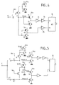
- FIG. 3 represents a preferred embodiment of the invention, making it possible to implement this security against noise in an extremely simple manner.
- the capacitance C is connected between the signal input E and the common input E 'of two inverters I1 and I2 each constituted by a set of two transistors serial; the bias voltage Vbias is supplied by a third inverter whose input is looped back to its output, the output providing the voltage Vbias.
- the inverter I1 comprises a P-channel MOS transistor T1 in series with an N-channel MOS transistor T'1.
- the P channel transistor is connected by its source to Vcc, the N channel transistor is connected by its source to ground; the gate of the P-channel transistor T1 is controlled by a reference voltage Vref.
- the gate of transistor T'1 constitutes the input of the inverter and is connected to terminal E '.
- the output of the inverter is taken from the combined drains of transistors T1 and T'1. It is it which is connected, by the intermediary or not of other inverters (I3, I4) to an input S1 of the flip-flop RS.
- the inverter I2 is constituted exactly like the inverter I1, with transistors T2 and T'2. However, as will be seen, the inverter I2 differs from the inverter I1 by the dimensions of its transistors.
- the output of the inverter I2, taken from the combined drains of T2 and T'2, is connected to the other input R1 of the flip-flop B.
- the third inverter previously mentioned which establishes the bias voltage Vbias on the input E ', comprises a transistor T3 (channel P) in series with a transistor T'3 (channel N) between the supply Vcc and the ground.
- the gate of transistor T3 is controlled by the same reference voltage Vref as the gates of transistors T1 and T2 of inverters I1 and I2.
- the gate of transistor T'3 is connected to the combined drains of T3 and T'3; it constitutes both the input and the output of the inverter, on which the bias voltage Vbias is automatically generated.
- This output is connected through a transistor Q (playing the role of resistance) to the input E 'of the inverters I1 and I2.
- Q is for example an N channel transistor having its gate connected to Vcc and having a small channel width / length ratio (so-called "long" transistor).
- the bias voltage Vbias is automatically determined by the voltage Vref and by the dimensions of the transistors T3 and T'3: the value Vref (or more exactly Vcc-Vref) imposes the current in the transistor T3, this current being proportional to the geometry of the transistor T3 for a given technology, that is to say for a given carrier mobility, a given gate oxide thickness, and a given threshold voltage of the transistors.
- This current, flowing in the transistor T'3 generates a gate-source voltage Vbias proportional to this current and inversely proportional to the geometry of the transistor T'3. It is therefore understood that Vbias is proportional to the ratio between the geometries of the transistors P and N of the inverter.
- inverters I1 and I2 the reference voltage Vref applied to the P-channel transistor and the bias voltage Vbias applied to the N-channel transistor would tend to impose a similar equilibrium in which the same current flows in the P-channel transistor and the N-channel transistor, if however the relationships between the geometries of the P-channel transistor and the N-channel transistor in these inverters were exactly the same as for the inverter T3, T'3.
- channel widths of transistors N in a ratio 27/20 between T1 and T3 and 17/20 between T2 and T3 are suitable.
- the inverters are also constituted by a P-channel transistor in series with an N-channel transistor between Vcc and ground; but instead of the P channel transistor having its gate connected to a reference voltage source Vref common to the three inverters, it has its gate connected to the gate of the N channel transistor, that is to say to the inverter input.
- the operation is the same and the value of the thresholds switching again depends on the ratios of the geometries of the N-channel and P-channel transistors for the different inverters: the ratio for the third inverter (T3, T'3) is between the corresponding ratios for the first two inverters (T1, T '1 and T2, T'2).
- a third inverter is used to define a bias voltage Vbias + v and a fourth inverter to define a bias voltage Vbias-v '.
- These bias voltages are applied one to the input E 'of the first inverter and the other to the input E' 'of the second; the inputs of the first two inverters are in fact disconnected and each connected by a respective capacitance C ', C' 'to the signal input E.
- the four inverters are constituted in the same way as in the embodiments already described, the fourth inverter comprising a P-channel transistor T4 in series with an N-channel transistor T'4.
- the first inverter preferably has geometries identical to those of the third and the second inverter has geometries of transistors identical to those of the fourth but slightly different from those of the first and third inverter, this difference establishing the difference between the bias voltages therefore between the switching thresholds of the inverters.
Landscapes
- Physics & Mathematics (AREA)
- Nonlinear Science (AREA)
- General Physics & Mathematics (AREA)
- Manipulation Of Pulses (AREA)
Claims (5)
- Gegen Rauschen geschützter Schwellenwertkomparator mit einem Signaleingang (E) zum Empfangen eines Signals mit variablem Pegel, gekennzeichnet durch wenigstens eine Eingangskapazität (C), die mit dem Signaleingang (E) verbunden ist, zwei Invertierglieder mit Schwellenwert (I1, 12), die jeweils einen mit dem Kondensator (C) verbundenen Eingang aufweisen, wobei diese Invertierglieder (I1, 12) nahe beieinanderliegende Kippschwellenwerte aufweisen, die einer Eingangsspannung Vbias + v für den einen und Vbias - v' für den anderen haben, wobei v und v' klein gegenüber der Versorgungsspannung Vcc des Komparators sind, wobei die Ausgänge der Invertierglieder (I1, 12) an einen Kippeingang eines Flipflops (B) vom Typ RS bzw. an den Rückstelleingang (R1) dieses Flipflops (B) angeschlossen sind, so daß bei einer Änderung des Zustandes eines der Invertierglieder als Folge des Überschreitens von Vbias + v durch das Eingangssignall das Kippen des Flipflops (B) und bei einer Änderung des Zustandes des anderen Invertierglieds als Folge der Rückkehr des Eingangssignals unter Vbias - v' das Rücksetzen hervorgerufen wird.
- Komparator nach Anspruch 1, dadurch gekennzeichnet, daß die Spannung Vbias durch den Ausgang wenigstens eines dritten Invertierglieds (T3, T'3) festgelegt wird, dessen Eingang mit seinem Ausgang verbunden ist, wobei dieser Ausgang mit den Eingängen der zwei ersten Invertierglieder verbunden ist, wobei jedes der drei Invertierglieder einen P-Kanal-Transistor in Serie mit einem N-Kanal-Transistor enthält und wobei die geometrischen Abmessungen (W/L) des P-Kanal-Transistors und des N-Kanal-Transistors jedes Invertierglieds so gewählt sind, daß das Verhältnis zwischen den geometrischen Abmessungen der Transistoren P und N (T1 und T'1) des ersten Invertierglieds geringfügig verschieden vom Verhältnis der geometrischen Parameter der Transistoren P und N (T2 und T'2) des zweiten Invertierglieds sind, während das Verhältnis zwischen den geometrischen Parametern der Transistoren P und N des dritten Invertierglieds zwischen den zwei ersten Verhältnissen liegen.
- Komparator nach Anspruch 2, dadurch gekennzeichnet, daß die Invertierglieder einen P-Kanal-Transistor enthalten, dessen Drain-Anschluß an eine Versorgungsspannung Vcc und dessen Gate-Anschluß an eine Referenzspannung Vref gelegt sind, und einen N-Kanal-Transistor enthalten, dessen Source-Anschluß an Masse liegt, dessen Gate-Anschluß den Eingang des Invertierglieds bildet und dessen Drain-Anschluß mit dem Drain-Anschluß des P-Kanal-Transistors verbunden ist, wobei die Referenzspannung Vref für alle Invertierglieder gleich ist, und wobei der Ausgang des Invertierglieds von den miteinander verbundenen Drain-Anschlüssen der zwei das Invertierglied bildenden Transistoren abgegriffen wird.
- Komparator nach Anspruch 2, dadurch gekennzeichnet, daß die Invertierglieder einen in Serie mit einem N-Kanal-Transistor liegenden P-Kanal-Transistor enthalten, wobei der Eingang des Invertierglieds von den miteinander verbundenen Gate-Anschlüssen der zwei Transistoren gebildet ist, während der Ausgang von den verbundenen Drain-Anschlüssen der Transistoren gebildet ist.
- Komparator nach einem der Ansprüche 2 bis 4, gekennzeichnet durch eine erste Kapazität (C'), die zwischen dem Signaleingang und dem Eingang eines ersten Invertierglieds angeschlossen ist, eine zweite Kapazität (C''), die zwischen dem Signaleingang und dem Eingang eines zweiten Invertierglieds angeschlossen ist, wobei der Komparator ein drittes Invertierglied enthält, dessen Eingang mit seinem Ausgang verbunden ist und das dazu dient, am Eingang des ersten Invertierglieds eine erste Vorspannung Vbias + v zu erzeugen, und ein viertes Invertierglied, dessen Eingang mit seinem Ausgang verbunden ist, um am Eingang des zweiten Invertierglieds eine zweite Vorspannung Vbias - v' zu erzeugen, wobei das Verhältnis zwischen den geometrischen Parametern der Transistoren, die das dritte Invertierglied bilden, vom Verhältnis der geometrischen Parameter der das vierte Invertierglied bildenden Transistoren verschieden ist.
Applications Claiming Priority (2)
| Application Number | Priority Date | Filing Date | Title |
|---|---|---|---|
| FR8916044 | 1989-12-05 | ||
| FR8916044A FR2655496B1 (fr) | 1989-12-05 | 1989-12-05 | Comparateur a seuil immunise contre le bruit. |
Publications (3)
| Publication Number | Publication Date |
|---|---|
| EP0447729A2 EP0447729A2 (de) | 1991-09-25 |
| EP0447729A3 EP0447729A3 (en) | 1992-05-06 |
| EP0447729B1 true EP0447729B1 (de) | 1993-05-19 |
Family
ID=9388160
Family Applications (1)
| Application Number | Title | Priority Date | Filing Date |
|---|---|---|---|
| EP90403391A Expired - Lifetime EP0447729B1 (de) | 1989-12-05 | 1990-11-29 | Gegen Rauschen geschützter Schwellwertdetektor |
Country Status (4)
| Country | Link |
|---|---|
| US (1) | US5170076A (de) |
| EP (1) | EP0447729B1 (de) |
| DE (1) | DE69001669T2 (de) |
| FR (1) | FR2655496B1 (de) |
Families Citing this family (10)
| Publication number | Priority date | Publication date | Assignee | Title |
|---|---|---|---|---|
| JP2928651B2 (ja) * | 1991-03-19 | 1999-08-03 | 株式会社日立製作所 | 通信機能を備えた制御装置 |
| US5341046A (en) * | 1992-12-07 | 1994-08-23 | Ncr Corporation | Threshold controlled input circuit for an integrated circuit |
| US5600270A (en) * | 1993-06-18 | 1997-02-04 | Yozan Inc. | Computational circuit |
| CN1108778A (zh) * | 1993-09-20 | 1995-09-20 | 株式会社鹰山 | 多极开关电路 |
| US5514987A (en) * | 1994-06-27 | 1996-05-07 | Advanced Micro Devices Inc. | Digital regenerative comparator |
| FI101328B (fi) * | 1997-04-18 | 1998-05-29 | Kone Oy | Menetelmä hissin kosketinpiirin toiminnan valvomiseksi |
| JP3596540B2 (ja) * | 2001-06-26 | 2004-12-02 | セイコーエプソン株式会社 | レベルシフタ及びそれを用いた電気光学装置 |
| KR100500928B1 (ko) * | 2002-06-29 | 2005-07-14 | 주식회사 하이닉스반도체 | 스위칭포인트 감지회로 및 그를 이용한 반도체 장치 |
| US7170329B2 (en) * | 2004-11-23 | 2007-01-30 | Faraday Technology Corp. | Current comparator with hysteresis |
| CN113608015B (zh) * | 2021-08-11 | 2024-04-09 | 南京导纳能科技有限公司 | 一种避雷器雷击动作的计数电路 |
Family Cites Families (8)
| Publication number | Priority date | Publication date | Assignee | Title |
|---|---|---|---|---|
| US3768024A (en) * | 1972-09-25 | 1973-10-23 | Gen Motors Corp | Zero crossover detector circuit |
| NL7805068A (nl) * | 1978-05-11 | 1979-11-13 | Philips Nv | Drempelschakeling. |
| JPS6019848B2 (ja) * | 1978-07-12 | 1985-05-18 | 株式会社日立製作所 | 電圧比較回路 |
| JPS5568729A (en) * | 1978-11-17 | 1980-05-23 | Mitsubishi Electric Corp | Input circuit with input level decision |
| JPS55136818A (en) * | 1979-04-11 | 1980-10-25 | Nippon Electric Co | Power voltage drop detecting circuit |
| US4521696A (en) * | 1982-07-06 | 1985-06-04 | Motorola, Inc. | Voltage detecting circuit |
| JPS5974721A (ja) * | 1982-10-21 | 1984-04-27 | Toshiba Corp | シユミツト・トリガ回路 |
| US4794283A (en) * | 1987-05-26 | 1988-12-27 | Motorola, Inc. | Edge sensitive level translating and rereferencing CMOS circuitry |
-
1989
- 1989-12-05 FR FR8916044A patent/FR2655496B1/fr not_active Expired - Lifetime
-
1990
- 1990-11-29 EP EP90403391A patent/EP0447729B1/de not_active Expired - Lifetime
- 1990-11-29 DE DE9090403391T patent/DE69001669T2/de not_active Expired - Fee Related
- 1990-12-04 US US07/624,088 patent/US5170076A/en not_active Expired - Lifetime
Also Published As
| Publication number | Publication date |
|---|---|
| FR2655496A1 (fr) | 1991-06-07 |
| US5170076A (en) | 1992-12-08 |
| DE69001669D1 (de) | 1993-06-24 |
| EP0447729A2 (de) | 1991-09-25 |
| EP0447729A3 (en) | 1992-05-06 |
| FR2655496B1 (fr) | 1992-02-28 |
| DE69001669T2 (de) | 1993-08-26 |
Similar Documents
| Publication | Publication Date | Title |
|---|---|---|
| EP0594834B1 (de) | In Standard-CMOS-Technologie realisierte, zwischen einer Logikschaltung mit niedriger Versorgungsspannung und einer Ausgangsstufe mit hoher Versorgungsspannung, liegende Schaltung | |
| EP1079525A1 (de) | System zur Steuerung eines Zweirichtungs-Schalters mit zwei Transistoren | |
| FR2749939A1 (fr) | Detecteur de gamme de tension d'alimentation dans un circuit integre | |
| EP0447729B1 (de) | Gegen Rauschen geschützter Schwellwertdetektor | |
| EP0700141B1 (de) | Temperaturdetektor auf einer integrierten Schaltung | |
| FR2529726A1 (fr) | Amplificateur a seuil prevu pour la fabrication en circuit integre | |
| EP0583203A1 (de) | Schaltung zum Ziehen des Eingangs einer integrierten Schaltung auf einen definierten Zustand | |
| EP1925079B1 (de) | Stromschalter mit durch eine niederspannung gespeisten differenztransistorpaaren | |
| EP0121464B1 (de) | Nichtflüchtige RAM Speicherzelle mit CMOS Transistoren mit gemeinsamem schwebendem Gate | |
| EP0568440B1 (de) | Detektionsschaltung mit Spannungsschwellen | |
| EP1672795A1 (de) | Vorrichtung zur Reinitialisierung eines integrierten Schaltkreises anhand der Detektion eines Spannungsabfalls der Stromversorgung und elektrische Schaltung hierfür | |
| EP0690573B1 (de) | Steuerschaltung für den teilweisen Standby-Betrieb einer Vorspannungsquelle | |
| CA2057824C (fr) | Dispositif de retard reglable | |
| EP0571302A1 (de) | Verstärker mit Ausgangsstrombegrenzung | |
| EP0699989B1 (de) | Integrierte Schaltung mit Sofortstartfunktion von Spannungsquellen oder Referenzstrom | |
| EP0368742B1 (de) | Digitalverstärker und diesen enthaltende integrierte Schaltung | |
| FR2534751A1 (fr) | Circuit de restauration a la mise sous tension pour un systeme de commande electrique | |
| EP0129470B1 (de) | Festkörper photoempfindliche Anordnung | |
| EP0480815B1 (de) | Integrierte Verstärkerschaltung mit einziger Eingangssignalverbindung | |
| EP0568474B1 (de) | MOS-Schaltung zum Extrahieren eines Synchronisierungssignals in einem BAS-Videosignal | |
| EP0715240B1 (de) | Spannungsregler für Logikschaltung in gekoppeltem Betriebszustand | |
| FR2767243A1 (fr) | Dispositif adaptateur symetrique de commutation d'un signal logique | |
| EP0332499B1 (de) | Schneller Komparator mit in zwei Phasen arbeitender Ausgangsstufe | |
| FR2549317A1 (fr) | Circuit de remise sous tension pour circuit logique | |
| EP0917288A1 (de) | Zelle mit Pseudo-Kapazität, insbesondere für künstliche Netzhaut |
Legal Events
| Date | Code | Title | Description |
|---|---|---|---|
| PUAI | Public reference made under article 153(3) epc to a published international application that has entered the european phase |
Free format text: ORIGINAL CODE: 0009012 |
|
| AK | Designated contracting states |
Kind code of ref document: A2 Designated state(s): DE FR GB IT |
|
| PUAL | Search report despatched |
Free format text: ORIGINAL CODE: 0009013 |
|
| AK | Designated contracting states |
Kind code of ref document: A3 Designated state(s): DE FR GB IT |
|
| 17P | Request for examination filed |
Effective date: 19920522 |
|
| 17Q | First examination report despatched |
Effective date: 19920721 |
|
| ITF | It: translation for a ep patent filed |
Owner name: ING. C. SPANDONARI |
|
| GRAA | (expected) grant |
Free format text: ORIGINAL CODE: 0009210 |
|
| AK | Designated contracting states |
Kind code of ref document: B1 Designated state(s): DE FR GB IT |
|
| REF | Corresponds to: |
Ref document number: 69001669 Country of ref document: DE Date of ref document: 19930624 |
|
| GBT | Gb: translation of ep patent filed (gb section 77(6)(a)/1977) |
Effective date: 19930722 |
|
| PLBE | No opposition filed within time limit |
Free format text: ORIGINAL CODE: 0009261 |
|
| STAA | Information on the status of an ep patent application or granted ep patent |
Free format text: STATUS: NO OPPOSITION FILED WITHIN TIME LIMIT |
|
| 26N | No opposition filed | ||
| REG | Reference to a national code |
Ref country code: FR Ref legal event code: D6 |
|
| PGFP | Annual fee paid to national office [announced via postgrant information from national office to epo] |
Ref country code: DE Payment date: 20001120 Year of fee payment: 11 |
|
| REG | Reference to a national code |
Ref country code: GB Ref legal event code: IF02 |
|
| PG25 | Lapsed in a contracting state [announced via postgrant information from national office to epo] |
Ref country code: DE Free format text: LAPSE BECAUSE OF NON-PAYMENT OF DUE FEES Effective date: 20020702 |
|
| PGFP | Annual fee paid to national office [announced via postgrant information from national office to epo] |
Ref country code: FR Payment date: 20021108 Year of fee payment: 13 |
|
| PGFP | Annual fee paid to national office [announced via postgrant information from national office to epo] |
Ref country code: GB Payment date: 20021127 Year of fee payment: 13 |
|
| PG25 | Lapsed in a contracting state [announced via postgrant information from national office to epo] |
Ref country code: GB Free format text: LAPSE BECAUSE OF NON-PAYMENT OF DUE FEES Effective date: 20031129 |
|
| GBPC | Gb: european patent ceased through non-payment of renewal fee |
Effective date: 20031129 |
|
| PG25 | Lapsed in a contracting state [announced via postgrant information from national office to epo] |
Ref country code: FR Free format text: LAPSE BECAUSE OF NON-PAYMENT OF DUE FEES Effective date: 20040730 |
|
| REG | Reference to a national code |
Ref country code: FR Ref legal event code: ST |
|
| PG25 | Lapsed in a contracting state [announced via postgrant information from national office to epo] |
Ref country code: IT Free format text: LAPSE BECAUSE OF NON-PAYMENT OF DUE FEES;WARNING: LAPSES OF ITALIAN PATENTS WITH EFFECTIVE DATE BEFORE 2007 MAY HAVE OCCURRED AT ANY TIME BEFORE 2007. THE CORRECT EFFECTIVE DATE MAY BE DIFFERENT FROM THE ONE RECORDED. Effective date: 20051129 |