EP0447225A2 - Verfahren und Einrichtung zur Maximierung von Spaltenadressenkohärenz für den Zugriff von seriellen und Direktzugriffstoren in einem graphischen System mit einem Rasterpufferspeicher - Google Patents
Verfahren und Einrichtung zur Maximierung von Spaltenadressenkohärenz für den Zugriff von seriellen und Direktzugriffstoren in einem graphischen System mit einem Rasterpufferspeicher Download PDFInfo
- Publication number
- EP0447225A2 EP0447225A2 EP91302152A EP91302152A EP0447225A2 EP 0447225 A2 EP0447225 A2 EP 0447225A2 EP 91302152 A EP91302152 A EP 91302152A EP 91302152 A EP91302152 A EP 91302152A EP 0447225 A2 EP0447225 A2 EP 0447225A2
- Authority
- EP
- European Patent Office
- Prior art keywords
- frame buffer
- graphics
- scan line
- scan
- display
- Prior art date
- Legal status (The legal status is an assumption and is not a legal conclusion. Google has not performed a legal analysis and makes no representation as to the accuracy of the status listed.)
- Granted
Links
Images

Classifications
-
- G—PHYSICS
- G09—EDUCATION; CRYPTOGRAPHY; DISPLAY; ADVERTISING; SEALS
- G09G—ARRANGEMENTS OR CIRCUITS FOR CONTROL OF INDICATING DEVICES USING STATIC MEANS TO PRESENT VARIABLE INFORMATION
- G09G5/00—Control arrangements or circuits for visual indicators common to cathode-ray tube indicators and other visual indicators
- G09G5/36—Control arrangements or circuits for visual indicators common to cathode-ray tube indicators and other visual indicators characterised by the display of a graphic pattern, e.g. using an all-points-addressable [APA] memory
- G09G5/39—Control of the bit-mapped memory
Definitions
- This invention relates to methods and apparatus for rendering graphics primitives to frame buffers in computer graphics systems. More specifically, this invention relates to methods and apparatus for maximizing performance of video random access memory (VRAM) arrays in graphics systems by maximizing column address coherency for serial and random port accesses in a frame buffer.
- VRAM video random access memory
- Computer graphics workstations can provide highly detailed graphics simulations for a variety of applications. Engineers and designers working in the computer aided design (CAD) and computer aided manufacturing (CAM) areas typically utilize graphics simulations for a variety of computational tasks. The computer graphics workstation industry has thus been driven to provide more powerful computer graphics workstations which can perform graphics simulations quickly and with increased detail.
- CAD computer aided design
- CAM computer aided manufacturing
- Modern workstations having graphics capabilities generally utilize "window" systems to accomplish graphics manipulations.
- computer workstation engineers have tried to design high performance, multiple window systems which maintain a high degree of user interactivity with the graphics workstation.
- a primary function of window systems in such graphics workstations is to provide the user with simultaneous access to multiple processes on the workstation. Each of these processes provides an interface to the user through its own area onto the workstation display.
- the overall result for the user is an increase in productivity since the user can then manage more than one task at a time with multiple windows displaying multiple processes on the workstation.
- graphics primitives are a basic component of a graphics picture, such as a polygon or vector. All graphics pictures are formed with combinations of these graphics primitives.
- Many schemes may be utilized to perform graphics primitives rendering.
- One such scheme is the "spline tessellation" scheme utilized in the TURBO SRX graphics system provided by the Hewlett Packard Graphics Technology division, Fort Collins, Colorado.
- a frame buffer generally comprises a plurality of video random access memory (VRAM) computer chips which store information concerning pixel activation on the system's display screen corresponding to the particular graphics primitives which will be traced out on the screen.
- VRAM video random access memory
- the frame buffer contains all the graphics data information which will be written onto the windows, and stores this information until the graphics system is prepared to trace this information on the workstation's screen.
- the frame buffer is generally dynamic and is periodically refreshed until the information stored on it is written to the screen.
- CTR cathode ray tube
- Display devices such as CRTs typically stimulate pixels sequentially in some regular order, such as left to right and top to bottom, and repeat the sequence 50 to 70 times a second to keep the screen refreshed. Thus, some mechanism is required to retain a pixel's value between the times that this value is used to stimulate the display.
- the frame buffer is typically used to provide this "refresh" function.
- Frame buffers for displaying data in windows on display screens in graphics rendering systems are known in the art. See U.S. Patent No. 4,780,709, Randall. As taught in the Randall patent, a display processor divides a display screen such as a CRT into a plurality of horizontal strips, with each strip being further subdivided into a plurality of "tiles.” Each tile represents a portion of a window to be displayed on the screen, and each tile is further defined by tile descriptors which include memory address locations of data to be displayed in that particular tile. See Randall, col. 2, lines 23-35.
- frame buffers are usually implemented as arrays of VRAMs, they are "bit mapped" such that pixel locations on a display device are assigned x,y coordinates on the frame buffer.
- a single VRAM device rarely has enough storage location to completely store all the x,y coordinates corresponding to pixel locations for the entire image on a display device, and therefore multiple VRAMs are generally used.
- the particular mapping algorithm used is a function of various factors, such as what particular VRAMs are available, how quickly the VRAM can be accessed compared to how quickly pixels can be rendered, how much hardware it takes to support a particular mapping, and other factors.
- Prior frame buffers in graphics systems comprised of VRAMs are generally dual port, random access memories.
- a serial output port develops the active video portion of a displayed video signal.
- signal processing circuitry accesses the VRAMs in the frame buffer via a standard input/output bus wherein the access is controlled by a VRAM control unit.
- data held in the VRAMs is provided to graphics processing circuitry which generally comprises decoders, first-in/first-out (FIFO) circuits, and an arithmetic and logic unit (ALU). See , e.g. , U.S. Patent No. 4,816,913 Harney et al. at col. 5, lines 27 through 62
- Generated pixel value data are written to the VRAMs in the frame buffer via output FIFOs in matrix form.
- the matrix corresponds to lines of video signal wherein each line has a separate number of pixel values.
- This matrix is referred to as the "bit map,” and is read from the VRAMs by a graphics display processor to produce an image on the graphics system display device.
- Display processors provide horizontal line synchronizing signals and vertical field synchronizing signals to coordinate transfer of data from the VRAMs to the display processor for ultimate display on a CRT. See Harney, col. 6, lines 7 through 24.
- Raster scan displays utilize a multiplicity of beams for simultaneously imaging data on a corresponding multiplicity of parallel scan lines.
- the multiplicity of beams usually write pixel value data to stimulate pixels on the display from the left side of the display CRT to the right side of the display CRT.
- each tile is considered to comprise a depth equal to the multiplicity of scan lines, with each tile being a particular number of pixels wide.
- the resulting graphics primitive image thus comprises a multiplicity of parallel, non-overlapping sets of parallel lines of pixels generated by a separate sweep of electron beams across the CRT screen.
- the tiles are generally rectangular, and thus organize the image into arrays having a plurality of rows by a set number of columns.
- raster scan displays are organized along scan lines wherein pixels in a display are activated according to the bit-mapped frame buffer coordinate pixel values.
- graphics primitives which potentially have random orientations and sizes are plotted on the raster display.
- the scanning raster CRT is accessed by the frame buffer according to row address strobe (RAS) and column address strobe (CAS) raster beams.
- RAS row address strobe
- CAS column address strobe
- Bit mapped systems generally utilize direct memory access (DMA) transfer sequences for transferring data from some external memory such as a ROM, cache buffer, or host processor to the VRAMs in the frame buffer.
- DMA direct memory access
- bit map systems are known as providing means for displaying characters and graphics patterns on CRT displays. See U.S. Patent no. 4,837,564, Ogawa et al., col. 1, lines 17 through 40.
- DMA transfer control is performed independently of processing control of graphics primitives attributes. Since a large number of hardware components are generally necessary for realizing DMA control sequences, the circuitry for such systems is complicated and the processing speed for expanding display data in a VRAM array may be reduced. In such systems, total processing speed for DMA sequences is not satisfactorily increased. See Ogawa et al., col. 1, lines 56 through 65. There is a long-felt need in the art for control data sequences for DMA transfer to increase processing speed, and to decrease the amount of expensive hardware necessary to perform this function.
- a display refresh port receives an incrementing address from the frame buffer, and the output data is first buffered then serialized using high speed shift registers typically built into the frame buffer architecture.
- the frame buffer then sends output data which drives digital to analog converters in a standard red/green/blue color monitor, or in a direct fashion to drive a black and white (monochrome) monitor. See U.S. Patent no. 4,745,407 Costello, col. 1, lines 32 through 55.
- a second update port, sometimes called a "random" port of the frame buffer is usually configured as an x,y random access memory wherein the frame buffer is organized into x,y coordinates.
- Knierim patent discloses a FIFO buffer which is provided to store sequences of data from a frame buffer and which comprises a barrel shifter to shift bit positions of the data words stored in the FIFO to facilitate proper pixel alignment during the horizontal scrolling operation. See col. 2, lines 3 through 7.
- Knierim patent improves page mode operation and performance in a frame buffer graphics system.
- further improvements with an eye toward maximizing page mode performance and column address coherency is desired in the art. This need must be satisfied without increasing the cost and complexity of the hardware necessary to form DMA transfer circuitry.
- the aforementioned long-felt needs are solved by methods and apparatus provided in accordance with the present invention.
- Methods and apparatus provided in accordance with the present invention satisfy the aforementioned long-felt needs in the computer graphics art for frame buffer graphic systems which have maximum column address coherency for serial and random port accesses in dual port, VRAM array frame buffers.
- the present invention maximizes page mode performance for VRAM arrays comprising frame buffers in graphic subsystems, or any other types of systems which utilize dual port VRAMs.
- processing time is greatly reduced, while system performance is enhanced for DMA transfer of data in graphics systems.
- methods of maximizing column address coherency for serial and random port accesses in a video random access memory array frame buffer which utilizes a raster scan device to display graphics primitives comprise the steps of organizing the video random access arrays into tiles, and shifting scan line data at a fixed interval across the raster scan display so that portions of scan line data are output to the raster scan CRT to display the graphics primitives.
- graphics display systems adapted to provide high performance page mode operation.
- the graphics display systems comprise raster scan display means having a plurality of scan lines for displaying graphics images, frame buffer means interfaced with the raster scan display means for mapping pixel value data corresponding to graphics primitives on the display means, the frame buffer means being organized into a plurality of rows and columns, random port means interfaced with the frame buffer means for outputting scan line data from a scan converter, serial port means interfaced with the frame buffer means for outputting scan line data to the raster scan display means and refreshing the raster scan display means with the pixel value data, and barrel shifting means interfaced with the serial port means for shifting the scan lines at a fixed interval so that the frame buffer partially outputs scan line data to the raster scan display means.
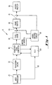
- Figure 1 is a graphics pipeline system provided in accordance with the present invention having a graphics frame buffer, raster scan display, and barrel shifting circuitry for maximizing column address coherency.
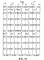
- Figure 2 is a bank of VRAM organized into a 4 X 4 tile in a graphics frame buffer.
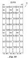
- Figures 3A and 3B illustrate a graphics frame buffer bit map organized into a plurality of rows and columns, wherein four scan lines access the bit mapped frame buffer.
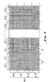
- Figure 4 is an illustration of a single row of the bit mapped frame buffer of figure 3.
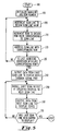
- Figure 5 is a flow chart of a preferred embodiment of methods provided in accordance with the present invention for maximizing column address coherency, and improving page mode performance of a graphics frame buffer system.
- Figure 1 depicts a frame buffer graphics system shown generally at 10.
- the frame buffer graphics system 10 in preferred embodiments is a pipeline graphics system wherein the graphics components are interconnected by pipeline hardware which performs a number of system tasks.
- a graphics pipeline is a series of data processing elements which communicate graphics commands through the graphics system.
- graphics pipelines with window architectures are evolving to support multitasking workstations.
- the graphics pipeline interconnects a host processor 20 to the graphics system which provides a multiplicity of graphics commands that are available to the system, and which also interfaces with the user.
- Host processor 20 is interfaced to a transform engine 30 along the graphics pipeline which generally comprises a number of parallel floating point processors.
- Transform engine 30 performs a number of system tasks including context management, matrix transformation calculations, light modeling and radiosity computations, and control of the systems's vector and polygon rendering hardware.
- Rendering circuit means 40 is further interfaced along the graphics pipeline with transform engine 30.
- rendering circuit means further comprises a scan converter.
- the scan converter is preferably a raster scan converter which controls RAS and CAS operations in the frame buffer and raster display in the graphics system.
- pixel cache means 50 is interfaced with the scan converter in rendering means 40.
- the pixel cache is generally a buffered memory which maintains pixel value data that is to be rendered to the frame buffer.
- a frame buffer 60 is further interfaced with pixel cache 50 along the pipeline graphics system.
- frame buffer 60 comprises a plurality of VRAM chips which are organized by the renderer and other graphics pipeline hardware into tiles to form graphics primitives.
- graphics primitives are basic shapes which comprise graphics figures that are displayed on the raster scan CRT.
- pixel value data can be manipulated so that the graphics primitives can be rendered to the CRT display.
- the tiles are rectangular, but may generally take on any arbitrary shape.
- frame buffer 60 is a dual port device.
- a serial port 70 interfaced with frame buffer 60 and raster display 80 provides scan output refresh data to the raster display.
- Random port 85 is interfaced with the frame buffer 60 and pixel cache 50 to provide updates of the graphics primitives and scenes which are rendered on frame buffer 60 and which will be displayed on raster display 80.
- barrel shifting means 90 is provided to the frame buffer 60 and is interfaced with renderer 40 containing the scan converter.
- barrel shifting means 90 comprises two barrel shifting circuits.
- a first barrel shifting circuit shifts data between pixel cache 50 and the random ports of the VRAMs into frame buffer 60.
- a second barrel shifting circuit shifts data between the VRAM serial ports and raster display 80. Control for the amount of shifting accomplished by the two barrel shifting circuits is preferably derived from the X-address of the rendered data or the refresh data respectively.
- scan line data can be vertically barrel shifted by barrel shifting circuitry 90 at fixed intervals across display 80 so that the scan line organized serial port 70 outputs data and maintains a much shorter page boundary for random port 85 accesses.
- barrel shifting circuitry 90 At fixed intervals across display 80 so that the scan line organized serial port 70 outputs data and maintains a much shorter page boundary for random port 85 accesses.
- barrel shifters in barrel shifter means 90 may be any barrel shifter circuit which is commonly available from the industry.
- Barrel shifting circuit 90 barrel shifts scan line data from frame buffer 60 to the raster display at a fixed interval as will be discussed herein. The fixed time interval determines when the barrel shifter means 90 allows scan line data from the frame buffer to be output to raster display 80.
- ALU 100 Interfaced with renderer 40 in the pipeline system 10 is an arithmetic logic unit (ALU) 100.
- ALU 100 is also interfaced with host processor 20 along a pipeline by-pass bus 110.
- ALU 100 performs various arithmetic functions such as, for example, window and source destination addressing, and conversion of window relative addresses from frame buffer relative addresses to raster display addresses.
- VRAM chips are shown having row designated letter values A through D, and numbered 0 to 3 in each of the rows. Thus, for example, in row A, VRAM chips are designated A0, A1, A2 and A3.
- pixel data words are stored in planes of the frame buffer memory array similar to the VRAM banks shown in Figure 2, and organized into tiles.
- each row may be stored.
- the sixteen bit data words in each row correspond to pixels in a raster line on the display device.
- the particular one of the sixteen words currently addressed in each tile is determined by the address bits for each of the rows, each of which are row and column address strobed.
- address bits for each of the rows each of which are row and column address strobed.
- a standard raster scanning technique is applied so that the graphics primitive and the pixel value data stored in the VRAMs of Figure 2 can be written to the display CRT. While a square tile has been illustrated in Figure 2, it will be recognized that any tile shape may be utilized with the methods and apparatus provided in accordance with the with the present invention as long as there is more than one scan line within a tile.
- a frame , buffer architecture 120 which is utilized in accordance with the present invention for maximizing column address coherency is split into a visible portion 130 in Figure 3A which corresponds to a raster display, and an off-screen, invisible portion 140 in Figure 3B which is generally viewed as a work area for window manipulation.
- the visible portion of the frame buffer is 1024 x 1280 x 8 bits while the invisible, off-screen area is 1024 x 768 x 8 bits.
- a single row address given to all VRAMs in the bank will enable page mode access to a 16 x 256 rectangle of pixels.
- scan line data which in preferred embodiments comprises four scan lines, can then be scanned out of the serial port so that the CRT can be stimulated to provide a graphics image.
- frame buffer 120 is partitioned so that visible region 130 is broken into five RAS zones denoted as RAS zone 0, RAS zone 1, RAS zone 2, RAS zone 3, and RAS zone 4.
- RAS zone the frame buffer VRAMs are broken into 64 columns.
- the invisible, off-screen region is partitioned into the remaining three RAS zones denoted as RAS zone 5, RAS zone 6, and RAS zone 7.
- Figure 4 illustrates which particular VRAM supplies data for a portion of a scan line, and which particular VRAM row and column addresses must be addressed to access a given pixel at an x,y location.
- square tiles are shown generally at 150.
- row 0 of the frame buffer addresses corresponding to 256 columns are illustrated.
- four scan lines must be used to output the scan line data through the dual port frame buffer to the display device so that the pixel value data can be rendered to the CRT.
- data for any given scan line is stored in two rows of VRAMs.
- scan line 0 data are stored in the row A VRAMs shown generally at 160, and the row C VRAMs shown generally at 170.
- the first 256 pixels come from the row A VRAMs while the next 256 pixels come from row C VRAMs. This allows 512 pixels (instead of 256 pixels) to be scanned out of the serial ports before the frame buffer VRAMs need to be reloaded.
- a single row address giving all the VRAMs in a bank will enable page mode access to a 16 x 256 rectangle of pixels.
- the source of data changes from one row of VRAM to another. If a 1 x 4 tile crosses the 256 pixel boundary, the data would not all come from one row of VRAM. Thus no 1 x 4 tile crosses any 256 pixel boundary on a single VRAM access cycle. If it does, the tile requires two VRAM cycles to access all four pixels. Otherwise, a 1 x 4 tile may start at any pixel.
- step 180 it is desired to initialize the row number and a particular scan line in the row. In further preferred embodiments, this initial value may be zero for both the scan line and row number.
- the scan line is incremented to obtain a scan line value
- the row number is incremented to obtain a row value corresponding to the scan line which will access the frame buffer so that data can be output to the CRT.
- the incrementing values at steps 200 and 210 give a particular row (N) and a scan line corresponding to a value, for example, "scan line A.”
- N row
- scan line A scan line A
- step 220 the scan line is addressed with the corresponding row number. It is then desired to determine at step 230 whether the last scan line has been addressed with the last corresponding row. If the answer to this question is "no," then the method returns to step 200 where incrementing of the scan line and the row numbers, and addressing of the scan line at steps 200, 210, and 220 can be repeated. For the 4 x 4 square tile discussed, incrementing occurs to obtain scan line B addressed with row (N + 1), scan line C addressed with row (N + 2), and scan line D addressed with row (N + 3). In preferred embodiments, once scan line D has been addressed with the (N + 3) row, at step 230 the last scan line has been addressed and the method proceeds.
- step 240 data is then output to the first scan line (scan line A) on the display device through the serial port of the frame buffer.
- the scan line output is then barrel shifted at a specified fixed interval to the next scan line, scan line B, at step 250.
- the data is then similarly output to scan line B at step 260 on the display device.
- step 270 it is determined whether data to the last scan line has been output from the frame buffer to the display.
- scan line B is not the last scan line to which data is output to the display device and so the method returns to step 250 where scan line B is barrel shifted to scan line C so that at step 260 scan line C output data can be bussed to the display device or CRT.
- the remaining scan lines can be barrel shifted at the fixed interval so that scan line D output data is also bussed to the display device.
- the method stops at 280.
- the fixed interval to activate the barrel shifter so that the scan lines can be switched is determined by taking the number of columns in the row divided by eight.
- the denominator "eight" is desired since there are preferably four rows represented along a scan line, and a factor of "two" is applied to the denominator since current VRAMs allow the serial port to be loaded with columns from two unique rows.
- This arrangement is denoted a "split shift register.”
- the RAS zones are changed at intervals of 16 so that scan output is switched from scan A to scan B to scan C to scan D at fixed intervals of 16 RAM access cycles.
Landscapes
- Engineering & Computer Science (AREA)
- Physics & Mathematics (AREA)
- Computer Hardware Design (AREA)
- General Physics & Mathematics (AREA)
- Theoretical Computer Science (AREA)
- Controls And Circuits For Display Device (AREA)
- Image Input (AREA)
- Image Generation (AREA)
Applications Claiming Priority (2)
| Application Number | Priority Date | Filing Date | Title |
|---|---|---|---|
| US494701 | 1990-03-16 | ||
| US07/494,701 US5233689A (en) | 1990-03-16 | 1990-03-16 | Methods and apparatus for maximizing column address coherency for serial and random port accesses to a dual port ram array |
Publications (3)
| Publication Number | Publication Date |
|---|---|
| EP0447225A2 true EP0447225A2 (de) | 1991-09-18 |
| EP0447225A3 EP0447225A3 (en) | 1992-12-23 |
| EP0447225B1 EP0447225B1 (de) | 1996-05-22 |
Family
ID=23965607
Family Applications (1)
| Application Number | Title | Priority Date | Filing Date |
|---|---|---|---|
| EP91302152A Expired - Lifetime EP0447225B1 (de) | 1990-03-16 | 1991-03-14 | Verfahren und Einrichtung zur Maximierung von Spaltenadressenkohärenz für den Zugriff von seriellen und Direktzugriffstoren in einem graphischen System mit einem Rasterpufferspeicher |
Country Status (4)
| Country | Link |
|---|---|
| US (1) | US5233689A (de) |
| EP (1) | EP0447225B1 (de) |
| JP (1) | JPH04222069A (de) |
| DE (1) | DE69119630T2 (de) |
Cited By (3)
| Publication number | Priority date | Publication date | Assignee | Title |
|---|---|---|---|---|
| EP0681279A3 (de) * | 1994-05-03 | 1996-01-17 | Sun Microsystems Inc | Direktzugriffspeicher und System für Rasterpuffer. |
| EP0681282A3 (de) * | 1994-05-03 | 1996-01-17 | Sun Microsystems Inc | Vielseitiger DRAM-Zugriff in einem Rasterpufferspeicher. |
| WO2000013145A1 (en) * | 1998-09-02 | 2000-03-09 | Silicon Graphics, Incorporated | Method and apparatus for rasterizing in a hierarchical order |
Families Citing this family (29)
| Publication number | Priority date | Publication date | Assignee | Title |
|---|---|---|---|---|
| JP2659614B2 (ja) * | 1990-11-13 | 1997-09-30 | 株式会社日立製作所 | 表示制御装置 |
| US5444845A (en) * | 1993-06-29 | 1995-08-22 | Samsung Electronics Co., Ltd. | Raster graphics system having mask control logic |
| US5815168A (en) * | 1995-06-23 | 1998-09-29 | Cirrus Logic, Inc. | Tiled memory addressing with programmable tile dimensions |
| US6031550A (en) * | 1997-11-12 | 2000-02-29 | Cirrus Logic, Inc. | Pixel data X striping in a graphics processor |
| US5999199A (en) * | 1997-11-12 | 1999-12-07 | Cirrus Logic, Inc. | Non-sequential fetch and store of XY pixel data in a graphics processor |
| US7365743B1 (en) * | 2002-10-08 | 2008-04-29 | Adobe Systems Incorporated | Assignments for parallel rasterization |
| US9330060B1 (en) | 2003-04-15 | 2016-05-03 | Nvidia Corporation | Method and device for encoding and decoding video image data |
| US8660182B2 (en) * | 2003-06-09 | 2014-02-25 | Nvidia Corporation | MPEG motion estimation based on dual start points |
| US20050062760A1 (en) * | 2003-07-09 | 2005-03-24 | Twede Roger S. | Frame buffer for non-DMA display |
| US7053808B2 (en) * | 2003-11-26 | 2006-05-30 | Texas Instruments Incorporated | Suppressing digital-to-analog converter (DAC) error |
| US7743085B2 (en) | 2004-11-08 | 2010-06-22 | Tabula, Inc. | Configurable IC with large carry chains |
| US7301368B2 (en) | 2005-03-15 | 2007-11-27 | Tabula, Inc. | Embedding memory within tile arrangement of a configurable IC |
| US7242216B1 (en) * | 2004-11-08 | 2007-07-10 | Herman Schmit | Embedding memory between tile arrangement of a configurable IC |
| US7825684B2 (en) | 2005-03-15 | 2010-11-02 | Tabula, Inc. | Variable width management for a memory of a configurable IC |
| US8731071B1 (en) * | 2005-12-15 | 2014-05-20 | Nvidia Corporation | System for performing finite input response (FIR) filtering in motion estimation |
| US7694083B1 (en) * | 2006-03-08 | 2010-04-06 | Tabula, Inc. | System and method for providing a virtual memory architecture narrower and deeper than a physical memory architecture |
| US7797497B1 (en) | 2006-03-08 | 2010-09-14 | Tabula, Inc. | System and method for providing more logical memory ports than physical memory ports |
| US8724702B1 (en) | 2006-03-29 | 2014-05-13 | Nvidia Corporation | Methods and systems for motion estimation used in video coding |
| US8660380B2 (en) * | 2006-08-25 | 2014-02-25 | Nvidia Corporation | Method and system for performing two-dimensional transform on data value array with reduced power consumption |
| US7930666B1 (en) | 2006-12-12 | 2011-04-19 | Tabula, Inc. | System and method of providing a memory hierarchy |
| US7587697B1 (en) | 2006-12-12 | 2009-09-08 | Tabula, Inc. | System and method of mapping memory blocks in a configurable integrated circuit |
| US20080291209A1 (en) * | 2007-05-25 | 2008-11-27 | Nvidia Corporation | Encoding Multi-media Signals |
| US8756482B2 (en) * | 2007-05-25 | 2014-06-17 | Nvidia Corporation | Efficient encoding/decoding of a sequence of data frames |
| US9118927B2 (en) * | 2007-06-13 | 2015-08-25 | Nvidia Corporation | Sub-pixel interpolation and its application in motion compensated encoding of a video signal |
| US8873625B2 (en) * | 2007-07-18 | 2014-10-28 | Nvidia Corporation | Enhanced compression in representing non-frame-edge blocks of image frames |
| US8666181B2 (en) * | 2008-12-10 | 2014-03-04 | Nvidia Corporation | Adaptive multiple engine image motion detection system and method |
| US9424444B2 (en) * | 2009-10-14 | 2016-08-23 | At&T Mobility Ii Llc | Systems, apparatus, methods and computer-readable storage media for facilitating integrated messaging, contacts and social media for a selected entity |
| WO2013071183A1 (en) | 2011-11-11 | 2013-05-16 | Tabula, Inc. | Content addressable memory in integrated circuit |
| US12511704B2 (en) | 2023-12-15 | 2025-12-30 | Samsung Electronics Co., Ltd. | Method for performing tile to raster (T2R) conversion in deep learning hardware accelerator |
Family Cites Families (14)
| Publication number | Priority date | Publication date | Assignee | Title |
|---|---|---|---|---|
| US4553171A (en) * | 1984-01-27 | 1985-11-12 | Xerox Corporation | Tile encoding in image printing |
| JPS60158484A (ja) * | 1984-01-28 | 1985-08-19 | 株式会社リコー | 表示メモリ制御方式 |
| US4701863A (en) * | 1984-12-14 | 1987-10-20 | Honeywell Information Systems Inc. | Apparatus for distortion free clearing of a display during a single frame time |
| US4755810A (en) * | 1985-04-05 | 1988-07-05 | Tektronix, Inc. | Frame buffer memory |
| JPS61254983A (ja) * | 1985-05-07 | 1986-11-12 | 株式会社ピーエフユー | 表示文字属性制御方式 |
| US4736442A (en) * | 1985-05-23 | 1988-04-05 | Kornfeld Cary D | System and method for orthogonal image transformation |
| US4777485A (en) * | 1985-09-13 | 1988-10-11 | Sun Microsystems, Inc. | Method and apparatus for DMA window display |
| US4745407A (en) * | 1985-10-30 | 1988-05-17 | Sun Microsystems, Inc. | Memory organization apparatus and method |
| US4780709A (en) * | 1986-02-10 | 1988-10-25 | Intel Corporation | Display processor |
| US4716546A (en) * | 1986-07-30 | 1987-12-29 | International Business Machines Corporation | Memory organization for vertical and horizontal vectors in a raster scan display system |
| US4816814A (en) * | 1987-02-12 | 1989-03-28 | International Business Machines Corporation | Vector generator with direction independent drawing speed for all-point-addressable raster displays |
| US4985848A (en) * | 1987-09-14 | 1991-01-15 | Visual Information Technologies, Inc. | High speed image processing system using separate data processor and address generator |
| US4835607A (en) * | 1987-11-16 | 1989-05-30 | Technology, Inc. | Method and apparatus for expanding compressed video data |
| US4816913A (en) * | 1987-11-16 | 1989-03-28 | Technology, Inc., 64 | Pixel interpolation circuitry as for a video signal processor |
-
1990
- 1990-03-16 US US07/494,701 patent/US5233689A/en not_active Expired - Lifetime
-
1991
- 1991-03-14 DE DE69119630T patent/DE69119630T2/de not_active Expired - Fee Related
- 1991-03-14 EP EP91302152A patent/EP0447225B1/de not_active Expired - Lifetime
- 1991-03-15 JP JP3051347A patent/JPH04222069A/ja active Pending
Cited By (5)
| Publication number | Priority date | Publication date | Assignee | Title |
|---|---|---|---|---|
| EP0681279A3 (de) * | 1994-05-03 | 1996-01-17 | Sun Microsystems Inc | Direktzugriffspeicher und System für Rasterpuffer. |
| EP0681282A3 (de) * | 1994-05-03 | 1996-01-17 | Sun Microsystems Inc | Vielseitiger DRAM-Zugriff in einem Rasterpufferspeicher. |
| US5544306A (en) * | 1994-05-03 | 1996-08-06 | Sun Microsystems, Inc. | Flexible dram access in a frame buffer memory and system |
| US7042460B2 (en) | 1998-07-02 | 2006-05-09 | Microsoft Corporation | Method and apparatus for rasterizing in a hierarchical tile order |
| WO2000013145A1 (en) * | 1998-09-02 | 2000-03-09 | Silicon Graphics, Incorporated | Method and apparatus for rasterizing in a hierarchical order |
Also Published As
| Publication number | Publication date |
|---|---|
| EP0447225B1 (de) | 1996-05-22 |
| DE69119630D1 (de) | 1996-06-27 |
| JPH04222069A (ja) | 1992-08-12 |
| EP0447225A3 (en) | 1992-12-23 |
| DE69119630T2 (de) | 1996-09-26 |
| US5233689A (en) | 1993-08-03 |
Similar Documents
| Publication | Publication Date | Title |
|---|---|---|
| US5233689A (en) | Methods and apparatus for maximizing column address coherency for serial and random port accesses to a dual port ram array | |
| US5251296A (en) | Methods and apparatus for generating arbitrarily addressed, arbitrarily shaped tiles in computer graphics systems | |
| US4225861A (en) | Method and means for texture display in raster scanned color graphic | |
| EP0087868B1 (de) | Bildwiederholspeicher-Architektur mit schnellem Zugriff für eine graphische Anzeigeeinrichtung | |
| US5266941A (en) | Apparatus and method for controlling storage of display information in a computer system | |
| US5012163A (en) | Method and apparatus for gamma correcting pixel value data in a computer graphics system | |
| EP0737956B1 (de) | Bildspeicher für graphische Daten | |
| EP0279228B1 (de) | Bildspeicher für Raster-Video-Anzeige | |
| US5457482A (en) | Method and apparatus for utilizing off-screen memory as a simultaneously displayable channel | |
| US5193148A (en) | Method and apparatus for pixel clipping source and destination windows in a graphics system | |
| US5696947A (en) | Two dimensional frame buffer memory interface system and method of operation thereof | |
| US5550961A (en) | Image processing apparatus and method of controlling the same | |
| US5561750A (en) | Z-buffer tag memory organization | |
| US5959638A (en) | Method and apparatus for constructing a frame buffer with a fast copy means | |
| US5371519A (en) | Split sort image processing apparatus and method | |
| US5321809A (en) | Categorized pixel variable buffering and processing for a graphics system | |
| US5859646A (en) | Graphic drawing processing device and graphic drawing processing system using thereof | |
| US5404448A (en) | Multi-pixel access memory system | |
| EP0279227B1 (de) | Vektorgenerator für Raster-Bildschirmanzeige | |
| EP0519694B1 (de) | Verfahren zur Zuteilung von Speicherplätzen ausserhalb des Bildschirms | |
| CA1312393C (en) | Method of tiling a figure in graphics rendering system | |
| US6031550A (en) | Pixel data X striping in a graphics processor | |
| JPH0782747B2 (ja) | ランダムアクセスポートおよびシリアルアクセスポートを有するメモリアレイ | |
| US5519413A (en) | Method and apparatus for concurrently scanning and filling a memory | |
| US4888584A (en) | Vector pattern processing circuit for bit map display system |
Legal Events
| Date | Code | Title | Description |
|---|---|---|---|
| PUAI | Public reference made under article 153(3) epc to a published international application that has entered the european phase |
Free format text: ORIGINAL CODE: 0009012 |
|
| AK | Designated contracting states |
Kind code of ref document: A2 Designated state(s): DE FR GB |
|
| PUAL | Search report despatched |
Free format text: ORIGINAL CODE: 0009013 |
|
| AK | Designated contracting states |
Kind code of ref document: A3 Designated state(s): DE FR GB |
|
| 17P | Request for examination filed |
Effective date: 19930217 |
|
| 17Q | First examination report despatched |
Effective date: 19940901 |
|
| GRAH | Despatch of communication of intention to grant a patent |
Free format text: ORIGINAL CODE: EPIDOS IGRA |
|
| GRAA | (expected) grant |
Free format text: ORIGINAL CODE: 0009210 |
|
| AK | Designated contracting states |
Kind code of ref document: B1 Designated state(s): DE FR GB |
|
| REF | Corresponds to: |
Ref document number: 69119630 Country of ref document: DE Date of ref document: 19960627 |
|
| ET | Fr: translation filed | ||
| PLBE | No opposition filed within time limit |
Free format text: ORIGINAL CODE: 0009261 |
|
| STAA | Information on the status of an ep patent application or granted ep patent |
Free format text: STATUS: NO OPPOSITION FILED WITHIN TIME LIMIT |
|
| 26N | No opposition filed | ||
| REG | Reference to a national code |
Ref country code: GB Ref legal event code: 732E |
|
| REG | Reference to a national code |
Ref country code: FR Ref legal event code: TP |
|
| REG | Reference to a national code |
Ref country code: GB Ref legal event code: IF02 |
|
| PGFP | Annual fee paid to national office [announced via postgrant information from national office to epo] |
Ref country code: DE Payment date: 20070430 Year of fee payment: 17 |
|
| PG25 | Lapsed in a contracting state [announced via postgrant information from national office to epo] |
Ref country code: DE Free format text: LAPSE BECAUSE OF NON-PAYMENT OF DUE FEES Effective date: 20081001 |
|
| PGFP | Annual fee paid to national office [announced via postgrant information from national office to epo] |
Ref country code: FR Payment date: 20100406 Year of fee payment: 20 |
|
| PGFP | Annual fee paid to national office [announced via postgrant information from national office to epo] |
Ref country code: GB Payment date: 20100326 Year of fee payment: 20 |
|
| REG | Reference to a national code |
Ref country code: GB Ref legal event code: PE20 Expiry date: 20110313 |
|
| PG25 | Lapsed in a contracting state [announced via postgrant information from national office to epo] |
Ref country code: GB Free format text: LAPSE BECAUSE OF EXPIRATION OF PROTECTION Effective date: 20110313 |