EP0446944A2 - Speiseschaltung für Fernmeldevermittlungsanlage - Google Patents
Speiseschaltung für Fernmeldevermittlungsanlage Download PDFInfo
- Publication number
- EP0446944A2 EP0446944A2 EP91104033A EP91104033A EP0446944A2 EP 0446944 A2 EP0446944 A2 EP 0446944A2 EP 91104033 A EP91104033 A EP 91104033A EP 91104033 A EP91104033 A EP 91104033A EP 0446944 A2 EP0446944 A2 EP 0446944A2
- Authority
- EP
- European Patent Office
- Prior art keywords
- digital signal
- feed circuit
- power
- circuit according
- feeding
- Prior art date
- Legal status (The legal status is an assumption and is not a legal conclusion. Google has not performed a legal analysis and makes no representation as to the accuracy of the status listed.)
- Withdrawn
Links
Images


Classifications
-
- H—ELECTRICITY
- H04—ELECTRIC COMMUNICATION TECHNIQUE
- H04M—TELEPHONIC COMMUNICATION
- H04M19/00—Current supply arrangements for telephone systems
- H04M19/001—Current supply source at the exchanger providing current to substations
- H04M19/005—Feeding arrangements without the use of line transformers
-
- H—ELECTRICITY
- H04—ELECTRIC COMMUNICATION TECHNIQUE
- H04M—TELEPHONIC COMMUNICATION
- H04M19/00—Current supply arrangements for telephone systems
- H04M19/001—Current supply source at the exchanger providing current to substations
Definitions
- the present invention relates to feed circuits, and more particularly to a feed circuit in an exchanger which supplies DC power to a subscriber line.
- FIG.1A shows a circuitry construction of a conventional so-called voltage driving type feed circuit and, and FIG.1B shows that of a conventional so-called current driving type feed circuit. Both circuits operates in substantially the same manner.
- the elements in FIG.1B which are the same as corresponding elements in FIG.1A are designated by the same reference numerals. Therefore, a description will be given below with reference to only FIG.1A.
- a power supply of -48V is connected to a collector of a transistor 501 and a noninverting input of an operational amplifier 521 via a resistor 511 having a resistance of R1.
- An output of the operational amplifier 521 is connected to a base of the transistor 501.
- An emitter of the transistor 501 is connected to the inverting input of the operational amplifier 521 and a terminal 541 which is connected to the subscriber line via a resistor 531 having a resistance of R e .
- the terminal 541 is connected to the noninverting input of the operational amplifier 521 via a resistor 551 having a resistance of R2.
- Another terminal 542 between the ground G and the subscriber line is connected to a circuit similar to that connected to the terminal 541, so that these elements of the circuit are designated by the same reference numerals each respectively having a subscript "2", and the description thereof will be omitted.
- the feed circuit in FIG.1B differs from that in FIG.1A in that each of the collectors of the transistors 501 and 502 are respectively directly connected to the terminals 541 and 542.
- the conventional feed circuit has the following disadvantage namely that as other elements should be added thereto every time there is a different need of a user so that it cannot be standardized for the various user's various needs.
- Another object of the present invention is to provide a feed circuit which can be standardized to satisfy various user's various needs.
- the feeding control means can automatically adjust the DC power by means of the feedback control every time there is a different need of a user, the feed circuit can be standardized for various user's needs.
- FIG.2 shows a block diagram for explaining the principle of the feed circuit.
- the feed circuit comprises, as shown in FIG.2, feeding means 11 and feeding control means 13.
- the feeding means 11 supplies the DC power to the subscriber line, and the DC power is adjusted based on the feedback voltage supplied from the feeding control means 13.
- the feeding means 13 obtains the DC power from joint points via a A/D convertor.
- the feeding control means 13 calculates the feedback voltage appropriate to a user's need by means of an operation process to fed it back to the feeding means 11 via a D/A convertor. Therefore, no additional element is required for the feed circuit to supply various user's various needs.
- FIGs.3A and 3B respectively show the circuitry constructions of the feed circuit in FIG.2. However both circuits operates in substantially the same manner.
- the feed circuit in FIG.3A corresponds to that in FIG.1A
- that in FIG.3B corresponds to that in FIG.1B.
- Those elements in FIG.3A which are the same as corresponding elements in FIG.3B are designated by the same reference numerals, and a description thereof will be omitted.
- the circuit in FIG.3A differs from that in FIG.1A in that a digital signal processor 21 in FIG.3A serves as the resistors 551 and 552 in FIG.1A to control the feeding means 11 by means of the digital operation process.
- the program input means 24 inputs a predetermined program appropriate to the user's need to the digital signal processor 21.
- the program input means 24 may be a read only memory (abbreviated ROM hereinafter) which stores some programs therein.
- a circuit connected to the power supply is the same as the circuit grounded, and the subscript of the reference numerals thereof will be omitted.
- the voltage outputted from the terminal 54 is converted into a digital signal by the A/D converter 22, and is inputted to the digital signal processor 21.
- the digital signal processor 21 determines a predetermined feedback voltage based on the predetermined program, and outputs a digital signal corresponding to the feedback voltage to the D/A converter 23.
- the D/A converter 23 generates the feedback voltage and inputs it to the noninverting input of the operational amplifier 52.
- FIG.4A shows a flowchart of the digital operation process executed by the digital signal processor 21 so that the DC power supplied from the feed circuit can reveal the constant-resistance characteristic.
- the digital signal processor 21 reads DC voltages V ia and V ib outputted from the feeding means 11 via the A/D converter 22 (in steps S1 and S4). In response to the DC voltages, it calculates respective feedback voltages V oa and V ob based on the predetermined program by means of the following equation (in steps S2 and S5): (V oa , V ob ) (V ia , V ib )*[R1/(R1+R2)].
- the [R1/(R1+R2)] indicates a feedback voltage ratio. Then, it transmits the feedback voltages to the D/A converter 23 (in steps S3 and S6).
- FIG.4B shows another flowchart executed by the digital signal processor 21 so that the DC power supplied from the feed circuit can reveal the constant-current characteristic.
- the processor performs the same operations as are performed in the steps S2 and S5 (in steps S9, S10, S14, and S15) so as to supply the desired constant current.
- FIG.5 shows a concrete block diagram of the feed circuit.
- the feed circuit comprises, as shown in FIG.5, voltage monitoring means 3, control signal generation means 4, and changable current supply means 5.
- the network 1 is connected to a pair of telephone lines 2.
- the telephone lines 2 are shorted out by resistors R c1 and R c2 .
- the voltage at a joint point of the resistors R c1 and R c2 is applied to the current control means 6.
- the voltage monitoring means 3 monitors the voltage applied to one of the telephone lines 2 to output a detecting signal corresponding to the voltage to the control signal generation means 4.
- the control signal generation means 4 generates the control signal corresponding to the detecting signal to transmit it to the changable feeding means 5.
- Various circuits used for the network 1 may be connected to terminals A and B.
- the voltage monitoring means 3 does not output the detecting signal to the control signal generation means 4. However, if a second line having a line-insulation resistance higher than that of the first line is substituted for the first line, the voltage monitoring means 3 outputs the detection signal to the control signal generation means 4, and the control signal generation means 4 outputs the control signal to the changable feeding means 5. As a result, the changable current supply means 5 changes the resistance thereof to decrease the current. If the current is still larger, the changable feeding means 5 continuously decreases the current. Thus, the extra current is lessened to the desired current value. On the other hand, if a third line having a line resistance lower than the first line is substituted for the first line, the current is increased to the desired current value by the same operation described above.
- FIG.6 shows a first circuitry construction of the feed circuit in FIG.5.
- the transformer T is coupled to a switching network (not shown), and primary coils thereof are connected to the terminals A and B via a pair of telephone lines having the line-insulation resistance RL.
- the transformer T may comprise a hybrid coil or a repeating coil. Since a capacitor C1 of the transformer T alternately connects the divided primary coils, DC is prevented from being supplied to the primary coils.
- the feed circuit supplies the constant current to the subsciber terminal.
- the feed circuit comprises operational amplifiers OPA, OPB, and OPC (simply referred to as OPA, OPB, and OPC hereinafter), a NPN type transistor QA, a PNP transistor QB, and resistors R A1 to RA 6 , R B1 to R B6 , and R C1 to R C4 .
- the resistors R A2 , R A4 , and R A5 are respectively directly connected to a power supply V BAT via switching circuits SW4, SW5, and SW6.
- the resistors R B2 , R B4 , and R B5 are respectively grounded via switching circuits SW1, SW2, and SW3. Incidentally, a plus terminal of the V BAT is grounded.
- one of the telephone lines is connected to minus input terminals of comparators CM1 and CM2 via the resistance R C4 , and is grounded via the resistors R C3 and R C4 and the capacitor C 2 .
- the resistor R C3 and the capacitor C 2 are connected in parallel.
- a plus input terminal of the comparator CM1 and a minus input terminal of the comparator CM2 are respectively connected to the threshold voltages V TH1 and V TH2 .
- the outputs of the comparators CM1 and CM2 are respectively connected to R and L input terminals of the control circuit (abbreviated CONT hereinafter), and outputs T1, T2, and T3 of the CONT are connected to the control signal input terminals of the switching circuits SW1 to SW6 (simply referred to as SW1 to SW6 hereinafter) via driving circuits DV1 and DV2 (simply referred to as DV1 and DV2).
- the loop monitoring circuit (abbreviated LOOP hereinafter) monitors a dial pulse or the ON/OFF condition of a handset of the telephone so as to transmit the pertinent information to the CONT, or to a CPU (not shown) via a scanner.
- the collector currents of the transistors QA and QB respectively become (R B6 *V BAT )/[2 * (R B6 +R B3 ) * R B1 ] and (R A6 * V BAT )/[2 * (R A6 +R A3 ) * R A1 ]. Therefore, the corrector currents of the Q A and Q B have the same value. That is, the current outputted from the Q A is inputted to the Q B .
- the currents of the Q A and Q B become constant irrespective of the line-insulation resistance RL, which exposes the constant-current characteristic.
- the SW1 to SW6 respectively connect the respective resistors R B6 and R A6 to one or some of the resistors R B2 , R B4 , R B5 , R A2 , R A4 , and R A5 . Therefore, the composite resistance decreases to change the constant current value
- the voltage V B of the terminal B is monitored by the comparators CM1 and CM2 via a low pass filter circuit comprising the resistors R C3 , R C4 , and the capacitor C 2 .
- the CM1 judges whether or not the voltage V B is more than the threshold V TH1
- the CM2 judges whether or not the voltage V B is less than the threshold V TH2 .
- the CM1 outputs a first detecting signal to the CONT so as to increase the current value if it judges the line-insulation resistance RL is too small.
- the CM2 outputs a second detecting signal to the CONT so as to decrease the current value if it judges the line-insulation resistance RL is too large.
- V BAT is -48V
- the maximum line-insulation resistance is 1900 ⁇
- four constant current values are respectively 20mA, 40mA, 60mA, and 80mA
- V TH1 is 16V
- V TH2 is 6.5V. If the line having a line-insulation resistance 600 , is initially connected to this feed circuit and the handset of the telephone is raised up, the LOOP outputs off hook information to the CONT and the scanner. Incidentally, the SW1 to SW6 are all initially opened.
- the feed circuit supplies the current 20mA to the terminals A and B
- the CM1 outputs the first detecting signal to the CONT since the voltage V B is higher than V TH1 .
- the CONT closes the SW1 and SW4 via the DV1 and DV2 in response to the first detecting signal.
- the resistors R B2 , R B4 , R B5 , and R B6 are connected in parallel with each other until the CM1 outputs the first detecting signal to the CONT. But the resistor R B2 is separated from other resistors R B4 , R B5 , and R B6 by means of the SW1.
- the CONT keeps the SW1 and SW4 closed.
- CM1 outputs the first detecting signal to the CONT, and the CONT closes the SW2 and SW5 via the DV1 and DV2.
- the CONT sets the current value at 60mA.
- the CONT resets the current value at 80mA, nevertheless as the current value 80mA is not enough, the CM1 continues to output the first detecting signal. But, in this case, the CONT ignores the first detecting signal, and keeps the operational condition of the feed circuit.
- the CM2 outputs the second detecting signal to the CONT.
- the CONT closes the SW3 and SW6 via the DV1 and DV2, and the CONT sets the current value at 60mA. Since the current value is not enough, the CM2 continues to output the second detecting signal, and thus the CONT resets the current value at 40mA. However, as the current value is not yet enough, the CM2 continuously outputs the second detecting signal. Finally, the CONT resets the current value at 20mA.
- the CONT keeps the SW1 to SW6 open.
- the desired constant current corresponding to the line-insulation resistance is set by the CONT so that the feed circuit can reveal the almost constant-resistance characteristic. The current value may be changed.
- FIG.7 shows a second circuitry construction of the feed circuit in FIG.5.
- the second circuitry construction thereof differs from the first one in that the resistors R B2 , R B4 , R B5 , R B6 , R A2 , R A4 , R A5 , and R A6 are directly connected. Therefore, the switching operation is different, needless to say. If the constant current value is 20mA, all switching circuits must be initially closed.
- Each switching circuit may comprise an analog switch, such as a relay or a CMOS.
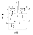
- FIG.10 shows an example of the circuitry construction of the CONT.
- Buffers IC1 and IC2 are constructed by the schmitt trigger circuit.
- One input terminal of an AND gate IC9 is connected to the buffer IC2, and another input terminal thereof is connected to the output of the LOOP.
- the output thereof is connected to an OR gate IC3 and one input terminal of an AND gate IC6.
- the output of the buffer IC1 is connected to another input terminal of the OR gate IC3 and one input terminal of an AND gate IC5.
- the output of the OR gate IC3 is connected to an input terminal of the timer IC4, and the output of the timer IC4 is connected to respective input terminals of the AND gates IC5 and IC6 via inverters.
- the output of the AND gate IC5 is connected to a mode select terminal S0 of a both-way shift register (74LSI94A), which is indicated as an up/down counter in FIG.10.
- the output of the AND gate IC6 is connected to another mode select terminal S1 of the both-way shift register IC7, and a clock generator (not shown) transmits the clock signal (8KHz) to a clock input terminal thereof.
- the parallel outputs Q A and Q B are connected to the terminals T1, T2 and T3.
- the outputs of terminals T1, T2, and T3 are directly supplied to the DV1 and DV2 in the feed circuit shown in FIG.6, whereas those are supplied to the DV1 and DV2 via inverters in the feed circuit shown in FIG.7.
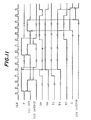
- FIG.11 shows a time chart showing the operation of the CONT in FIG.10.
- a signal "1" (simply referred to as "1"
- the timer outputs a signal to the timer IC4 to drive the timer IC4 via the buffer IC1 and the OR gate IC3. Since the voltage V B changes greatly based on the dial signal, the timer outputs an output signal to the AND gates IC5 and IC6 after 1 second to prevent the malfunctioning of the CONT.
- the AND gate IC5 outputs "1" to the both-way shift register IC7 to shift it to the right and make it output the "1" to the terminal T1.
- the timer IC4 After 1 second, the timer IC4 outputs the output signal to the AND gate IC5, and it outputs the "1". Thus, the both-way shift register IC7 is shifted to the right to output "1" to the terminal T3. In response to the R input terminal set at "0", the AND gate IC5 outputs "0" to stop the operating of the both-way shift register IC7.
- FIG.12 shows another example of the circuitry construction of the CONT.
- the buffers IC1 and IC2 are respectively constructed by the schmitt trigger circuits, and the output of the buffer IC2 is inputted to one input terminal of the AND gate IC9.
- the SCN signal is inputted to another input terminal of the AND gate IC9.
- the output of the AND gate IC9 is connected to input terminals of the OR gate IC3 and the AND gate IC6.
- the output of the buffer IC1 is connected to one input terminal of the AND gate IC5.
- the output of the OR gate IC3 is inputted to the input terminal of the timer IC4.
- the output of the timer IC4 is connected to the input terminals AND gates IC5 and IC6 via the inverters.
- the respective outputs of the AND gate IC5 and IC6 are respectively connected to the respective input terminals of the AND gates IC8 and IC10.
- the other input terminals of the AND gates IC8 and IC10 are respectively connected to a clock generator (not shown) so that the clock signal (8KHz) is inputted to each of the input terminals thereof.
- the output of the AND gate IC8 is connected to a count up terminal UP of the up/down counter (74LSI192) IC11, and the output of the AND gate IC10 is connected to a count down terminal DOWN of the up/down counter IC11.
- the output Q A of the up/down counter IC11 is connected to one input terminal of the AND gate IC13 so that the output Q B of the up/down counter IC11 is connected to input terminals of the OR gate IC12 and the AND gate IC13.
- the output of the OR gate IC12 is connected to the terminal T1, and the output of the AND gate IC13 is connected to the terminal T3.
- the terminals T1, T2, and T3 are connected to the DV1 and DV2.
- the outputs from the terminals T1, T2, and T3 in FIG.6 are directly inputted to the DV1 and DV2, whereas those in FIG.7 are inputted via the inverters.
- the signal When "1" is inputted to the R input terminal, the signal is inputted to the timer IC4 to drive it via the buffer IC1 and the OR gate IC3.
- the timer outputs the output signal 1 second after the time it is driven, and the AND gate IC5 outputs "1" to the AND gate IC8 to open the AND gate IC8.
- the clock signal is inputted to the count up terminal up via the AND gate IC8.
- the up/down counter IC11 counts up, and the output terminal Q A thereof becomes “1” whereas the output terminal Q B thereof “0". Therefore, only the terminal T1 outputs "1” .
- the AND gate IC6 outputs "0" to interrupt the clock signal transmitted from the AND gate IC10.
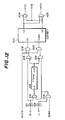
- FIG.13 shows the respective circuitry construction of the DV1, DV2, and the switching circuits SW1 to SW6.
- the feed circuits respectively indicated in FIGs.6 and 7 use three circuits shown in FIG.13.
- the terminal Tx is connected to terminals T1, T2, and T3.
- the terminal DVx is connected to one of the resistors R B2 , R B4 , and R B5 .
- the terminal DVy is connected to one of the resistors R A2 , R A4 , and R A5 .
- the terminal Tx is connected to one end of the resistor R dV2 , and another end thereof is connected to a base of the transistor Q dV1 .
- the base of the transistor Q dV1 is connected to a plus terminal of the power supply (5V).
- An emitter of the transistor Q dV1 is connected to the plus terminal of the power supply.
- the collector of the transistor Q dV1 is connected to V BAT via the resistors R dV3 and R dV4 , and the joint point of the resistors R dV3 and R dV4 is connected to the base of the transistor Q dV2 .
- the emitter of the transistor Q dV2 is connected to the V BAT , and the collector of the transistor Q dv2 is grounded via the resistors R dV6 and R dV5 .
- the joint point of the resistors R dV6 and R dV5 is connected to the base of the transistor Q SWX .
- the emitter of the transistor Q SWX is grounded, and the collector thereof is connected to the terminal DVx.
- the collector of the transistor Q dV1 is connected to the V BAT via the resistors R dV7 and R dV8 , and the joint point of the and resistors R dV7 and R dV8 is connected to the base of the transistor Q SWY .
- the emitter of the transistor Q SWY is connected to the V BAT , and the collector thereof is connected to the terminal Dvy.
- the current is supplied to the base of the transistor Q SWY via the resistor R dV7 in response to the switching on of the transistor Q dV1 so that transistor Q SWY is switched on.
- the terminal Tx becomes "1”
- the transistor Q dV1 is switched off, and thus the transistor Q dV2 is switched off.
- the transistor Q SWY is switched off.
- the terminal DVx is shorted out to be grounded or opened
- the terminal DVy is shorted out of the V BAT or opened because of input information which is inputted to the terminal Tx to switch the driving circuit and the switching circuit.
- the transistor Q SWX corresponds to the SW1 to SW3
- the transistor Q SWY corresponds to the SW4 to SW6.
- the DV1 and DV2 are combined in FIG.13.
- FIG.14 shows a detailed circuit constructions of the DV1, DV2, and SW1 to SW6.
- the second and third embodiments in FIGs.6 and 7 use three pairs of circuit shown in FIG.14 .
- a terminal Tx is respectively connected to the terminals T1, T2, and T3 of the CONT.
- the terminal DVx is connected to one of the resistors R B2 , R B4 , and R B5 .
- the terminal DVy is connected to one of the resistances R A2 , R A4 , and R A5 .
- the terminal Tx is connected to one end of the resistance R dV2 , and another end thereof is connected to a base of the transistor Q dV1 .
- the base of the transistor Q dV1 is connected to a plus terminal of the power source (5V).
- an emitter of the transistor Q dV1 is connected to the plus terminal of the power source.
- the collector of the transistor Q dV1 is connected to the V BAT via the resistances R dV3 and R dV4 , and the joint point of the resistances R dV3 and R dV4 is connected to the base of the transistor Q SWX .
- the emitter of the transistor Q SWX is connected to the V BAT , and the collector of the transistor Q SWY is connected to the transistor Q SWX via the resistance R SW2 and to the terminal DVy.
- the base and emitter of the transistor Q SWX are grounded, and the collector thereof is connected to the terminal DVx.
- the base current is supplied to the transistor Q dV1 via the resistance R dV2 , so that the transistor Q dV1 switched on. Then the current is supplied to the base of the transistor Q SWY to switch it on. Thus, the base current of the transistor Q SWX is supplied via the resistance R SW2 , and the transistor Q SWX is switched on.
- the terminal DVx is shorted out to be grounded or opened, and the terminal DVy is shorted out to the V BAT or opened because input information of the terminal TX is inputted so as to switch the driving circuit and the switching circuit.
- the transistor Q SWX corresponds to the SW1 to SW3
- the transistor Q SWY corresponds to the SW4 to SW6.
- the DV1 and DV2 are combined in FIG.14.
- FIG.15 shows detailed circuit constructions of the DV1, DV2, and SW1 to SW6.
- the second and third embodiments in FIGs.6 and 7 use the three pairs of circuit shown in FIG.14.
- a terminal Tx is respectively connected to the terminals T1, T2, and T3.
- the terminal DVx is connected to one of the resistors R B2 , R B4 , and R B5 .
- the terminal DVy is connected to one of the resistors R A2 , R A4 , and R A5 .
- the terminal Tx is connected to one end of the resistor R dV2 , and another end thereof is connected to a base of the transistor Q dV1 .
- the base of the transistor Q dV1 is connected to a plus terminal of the power source (5V).
- an emitter of the transistor Q dV1 is connected to the plus terminal of the power source.
- the collector of the transistor Q dV1 is connected to the V BAT via the resistors R dV3 and R dV4 , and the joint point of the resistors R dV3 and R dV4 is connected to the base of the transistor Q dV2 .
- the emitter of the transistor Q dV2 is connected to the V BAT , and the collector of the transistor Q dV2 is grounded via the resistor R dV5 .
- the collector of the transistor Q dV2 is respectively connected to control input terminals of the analog switches ASWX and ASWY.
- the controlled electrode of the analog switch ASWX is grounded, and the controlled electrode of the analog switch ASWX is connected to the terminal DVx.
- the controlled electrode of the analog switch ASWY is connected to the V BAT , and another controlled electrode of the analog switch ASWY is connected to the terminal DVy.
- the base current is supplied to the transistor Q dV1 via the resistance R dV2 , so that the transistor Q dV1 is turned on. Then the transistor Q dV2 is switched on, and the analog switches ASWX and ASWY are turned on, respectively.
- the terminal DVx is shorted out to be grounded or opened, and the terminal DVy is shorted out to the V BAT or opened because input information of the terminal TX is outputted so as to switch the driving circuit and the switching circuit.
- the analog switch ASWX corresponds to the SW1 to SW3
- the analog switch ASWY corresponds to the SW4 to SW6.
- the DV1 and DV2 are combined in FIG.15.
- FIG 16 shows a flowchart showing how the DC power in the feed circuit in FIG.2 reveal the same characteristic as that in the feed circuit in FIG.5. Therefore, the feed circuit in FIG.2 can serve as that in FIG.5.
- the digital signal processor 21 reads and judges the level of the L and SCN terminals (in steps S25 and S26). If both L and SCN terminals are "1", then the digital signal processor 21 judges whether or not the S is larger than 0 (in step S27). If S>0, the digital signal processor 21 subtracts 1 from S (in step S28). However, if both L and SCN terminals are not "1" or S ⁇ 0 (in the steps S26 and S27), then the digital signal processor 21 respectively outputs predetermined values to the terminals T1, T2, and T3 based on the value of S (in steps S29 to S33).
Landscapes
- Engineering & Computer Science (AREA)
- Signal Processing (AREA)
- Power Engineering (AREA)
- Devices For Supply Of Signal Current (AREA)
Applications Claiming Priority (4)
| Application Number | Priority Date | Filing Date | Title |
|---|---|---|---|
| JP2066701A JPH03268558A (ja) | 1990-03-16 | 1990-03-16 | 給電制御方式 |
| JP66701/90 | 1990-03-16 | ||
| JP2068147A JPH03270460A (ja) | 1990-03-20 | 1990-03-20 | 定電流給電回路 |
| JP68147/90 | 1990-03-20 |
Publications (2)
| Publication Number | Publication Date |
|---|---|
| EP0446944A2 true EP0446944A2 (de) | 1991-09-18 |
| EP0446944A3 EP0446944A3 (en) | 1991-12-27 |
Family
ID=26407888
Family Applications (1)
| Application Number | Title | Priority Date | Filing Date |
|---|---|---|---|
| EP19910104033 Withdrawn EP0446944A3 (en) | 1990-03-16 | 1991-03-15 | Feed circuit in exchanger |
Country Status (3)
| Country | Link |
|---|---|
| EP (1) | EP0446944A3 (de) |
| AU (1) | AU7354291A (de) |
| CA (1) | CA2038376A1 (de) |
Cited By (9)
| Publication number | Priority date | Publication date | Assignee | Title |
|---|---|---|---|---|
| EP0663755A1 (de) * | 1994-01-17 | 1995-07-19 | Siemens Aktiengesellschaft | Schaltungsanordnung zur Speisung einer Teilnehmeranschlussleitung |
| EP0670651A1 (de) * | 1994-03-04 | 1995-09-06 | Siemens Aktiengesellschaft | Schaltungsanordnung zur Gleichspannungsspeisung einer Fernsprechleitung |
| GB2315188A (en) * | 1996-07-09 | 1998-01-21 | Telspec Plc | Telephone power supply |
| WO1998008336A1 (en) * | 1996-08-21 | 1998-02-26 | Advanced Micro Devices, Inc. | Digital direct current feed control for a communication system |
| WO1998013999A3 (en) * | 1996-09-26 | 1998-06-18 | Jacob Mulder | Power supply circuit, telecommunication device and method for multiple dc slope power management |
| WO2001030062A1 (en) * | 1999-10-20 | 2001-04-26 | Legerity, Inc. | Method and apparatus for dc feed control |
| EP1017211A3 (de) * | 1998-12-31 | 2003-06-25 | STMicroelectronics S.r.l. | Monolitisch integrierte Teilnehmerschaltungsanordnung zur treiben einer Breitbandleitung für datenübertragung |
| EP0808053A3 (de) * | 1996-05-10 | 2003-08-13 | Lucent Technologies Inc. | Selbstüberwachende Teilnehmerschaltung |
| US6678377B1 (en) | 1998-12-31 | 2004-01-13 | Stmicroelectronics S.R.L. | Monolithically integrated telephone circuit for driving wide-band telephone lines for data transmission |
Family Cites Families (2)
| Publication number | Priority date | Publication date | Assignee | Title |
|---|---|---|---|---|
| US3916110A (en) * | 1974-05-02 | 1975-10-28 | Gte Automatic Electric Lab Inc | Line circuit employing constant current devices for battery feed |
| US3993880A (en) * | 1976-02-09 | 1976-11-23 | Bell Telephone Laboratories, Incorporated | Resistive battery feed for line circuits |
-
1991
- 1991-03-15 AU AU73542/91A patent/AU7354291A/en not_active Abandoned
- 1991-03-15 EP EP19910104033 patent/EP0446944A3/en not_active Withdrawn
- 1991-03-15 CA CA 2038376 patent/CA2038376A1/en not_active Abandoned
Cited By (12)
| Publication number | Priority date | Publication date | Assignee | Title |
|---|---|---|---|---|
| EP0663755A1 (de) * | 1994-01-17 | 1995-07-19 | Siemens Aktiengesellschaft | Schaltungsanordnung zur Speisung einer Teilnehmeranschlussleitung |
| EP0670651A1 (de) * | 1994-03-04 | 1995-09-06 | Siemens Aktiengesellschaft | Schaltungsanordnung zur Gleichspannungsspeisung einer Fernsprechleitung |
| EP0808053A3 (de) * | 1996-05-10 | 2003-08-13 | Lucent Technologies Inc. | Selbstüberwachende Teilnehmerschaltung |
| GB2315188A (en) * | 1996-07-09 | 1998-01-21 | Telspec Plc | Telephone power supply |
| GB2315188B (en) * | 1996-07-09 | 1999-04-14 | Telspec Plc | Power supply system for telephone line wires |
| WO1998008336A1 (en) * | 1996-08-21 | 1998-02-26 | Advanced Micro Devices, Inc. | Digital direct current feed control for a communication system |
| US5878133A (en) * | 1996-08-21 | 1999-03-02 | Advanced Micro Devices, Inc. | Digital direct current feed control for a communication system |
| WO1998013999A3 (en) * | 1996-09-26 | 1998-06-18 | Jacob Mulder | Power supply circuit, telecommunication device and method for multiple dc slope power management |
| EP1017211A3 (de) * | 1998-12-31 | 2003-06-25 | STMicroelectronics S.r.l. | Monolitisch integrierte Teilnehmerschaltungsanordnung zur treiben einer Breitbandleitung für datenübertragung |
| US6678377B1 (en) | 1998-12-31 | 2004-01-13 | Stmicroelectronics S.R.L. | Monolithically integrated telephone circuit for driving wide-band telephone lines for data transmission |
| WO2001030062A1 (en) * | 1999-10-20 | 2001-04-26 | Legerity, Inc. | Method and apparatus for dc feed control |
| US6671373B1 (en) | 1999-10-20 | 2003-12-30 | Legerity, Inc. | Method and apparatus for DC feed control |
Also Published As
| Publication number | Publication date |
|---|---|
| EP0446944A3 (en) | 1991-12-27 |
| CA2038376A1 (en) | 1991-09-17 |
| AU7354291A (en) | 1991-11-14 |
Similar Documents
| Publication | Publication Date | Title |
|---|---|---|
| US4317963A (en) | Subscriber line interface circuit utilizing impedance synthesizer and shared voltage source for loop current regulation control | |
| EP0446944A2 (de) | Speiseschaltung für Fernmeldevermittlungsanlage | |
| US5511118A (en) | Method of providing d.c. feed to a telephone line | |
| CA1173578A (en) | Subscriber line interface circuit with impedance synthesizer | |
| EP0455893B1 (de) | Fernmeldeleitungsschaltung | |
| AU707018B2 (en) | A transmission method | |
| CA1292588C (en) | Subscriber line interface circuit | |
| US6731728B2 (en) | Low noise line powered DAA with differential feedback | |
| JPS63169864A (ja) | 電話インタフェース回路のための直流制御回路 | |
| EP0273922B1 (de) | Vorrichtung in einem fernübertragungssystem für stromversorgung eines fernsprechersatzes | |
| DK165614B (da) | Telefonstroemforsyning | |
| US6421430B1 (en) | Line powered DAA with single ended feedback | |
| JPH07297886A (ja) | 電話線インターフェース回路 | |
| JP2000134648A (ja) | プログラム可能な電話加入者ル―プインタ―フェ―ス回路(slic)及び方法 | |
| US4723278A (en) | Voice circuit of telephone | |
| JPS61154348A (ja) | 給電々流制限方式 | |
| JP3487839B2 (ja) | 網制御装置 | |
| JP3461214B2 (ja) | Dc/dcコンバータ | |
| JPH0746283B2 (ja) | 制御回路 | |
| JPS6216059B2 (de) | ||
| JPS615670A (ja) | 通話電流供給回路 | |
| JPH0351350B2 (de) | ||
| EP0419935A3 (en) | Subscriber connecting circuit for the connection of a subscriber line to the exchange of a digital time division multiplex communication system | |
| JPH025349B2 (de) | ||
| GB2296581A (en) | Limited power systems |
Legal Events
| Date | Code | Title | Description |
|---|---|---|---|
| PUAI | Public reference made under article 153(3) epc to a published international application that has entered the european phase |
Free format text: ORIGINAL CODE: 0009012 |
|
| AK | Designated contracting states |
Kind code of ref document: A2 Designated state(s): DE FR GB |
|
| PUAL | Search report despatched |
Free format text: ORIGINAL CODE: 0009013 |
|
| AK | Designated contracting states |
Kind code of ref document: A3 Designated state(s): DE FR GB |
|
| 17P | Request for examination filed |
Effective date: 19920421 |
|
| 17Q | First examination report despatched |
Effective date: 19940314 |
|
| STAA | Information on the status of an ep patent application or granted ep patent |
Free format text: STATUS: THE APPLICATION IS DEEMED TO BE WITHDRAWN |
|
| 18D | Application deemed to be withdrawn |
Effective date: 19940927 |