EP0446724A2 - Verfahren und Vorrichtung zur Strombegrenzung - Google Patents
Verfahren und Vorrichtung zur Strombegrenzung Download PDFInfo
- Publication number
- EP0446724A2 EP0446724A2 EP91103101A EP91103101A EP0446724A2 EP 0446724 A2 EP0446724 A2 EP 0446724A2 EP 91103101 A EP91103101 A EP 91103101A EP 91103101 A EP91103101 A EP 91103101A EP 0446724 A2 EP0446724 A2 EP 0446724A2
- Authority
- EP
- European Patent Office
- Prior art keywords
- network
- voltage source
- resistors
- fusible link
- providing
- Prior art date
- Legal status (The legal status is an assumption and is not a legal conclusion. Google has not performed a legal analysis and makes no representation as to the accuracy of the status listed.)
- Granted
Links
Images
Classifications
-
- H—ELECTRICITY
- H02—GENERATION; CONVERSION OR DISTRIBUTION OF ELECTRIC POWER
- H02H—EMERGENCY PROTECTIVE CIRCUIT ARRANGEMENTS
- H02H3/00—Emergency protective circuit arrangements for automatic disconnection directly responsive to an undesired change from normal electric working condition with or without subsequent reconnection ; integrated protection
- H02H3/006—Calibration or setting of parameters
-
- H—ELECTRICITY
- H02—GENERATION; CONVERSION OR DISTRIBUTION OF ELECTRIC POWER
- H02H—EMERGENCY PROTECTIVE CIRCUIT ARRANGEMENTS
- H02H9/00—Emergency protective circuit arrangements for limiting excess current or voltage without disconnection
- H02H9/02—Emergency protective circuit arrangements for limiting excess current or voltage without disconnection responsive to excess current
- H02H9/025—Current limitation using field effect transistors
Definitions
- the present invention relates to the field of electronic devices and their manufacture. More specifically, in one embodiment the invention provides a method and apparatus for limiting current flow for the purpose of, for example, protection, control, signal generation, and the like.
- Such current limiters could be used in a wide variety of applications which include, but are by no means limited to, protection, control, signal generation.
- a current limiter provides an output current which is largely independent of an input voltage. In reality, most such devices do not begin to operate effectively until the voltage between their terminals reaches some minimum voltage, generally referred to as V t . Their performance begins to deteriorate above some breakdown voltage, V bd .
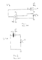
- Fig. 1 illustrates a typical current limiting device 2.
- the current I s is to be regulated.
- the current limiting device includes an enhancement mode HVFET 4 which is driven in a closed loop mode via a shunt resistor 6 and an amplifier 8.
- the current I s will, within limits, be set by the resistance of the shunt resistor 6 and will be largely independent of the voltage applied at the point "D.”
- I s will equal approximately V t /R s where V t is roughly the threshold voltage of the FET 4.
- Such current limiting devices have the disadvantage of, for example, being complex. In the device shown in Fig. 1, for example, it is necessary to provide a power supply for V cc , an op-amp 8, a transistor 4, a resistor 6, and the like.
- Fig. 2 illustrates another type of current source in which a depletion mode FET 10 is utilized.
- the current is "on" when the gate of the FET is shorted to the source.
- I D is set by processing conditions in the fabrication of the device and, in particular, the design of the FET and the resistors. Accordingly, users of such devices frequently purchase a transistor 10 and select a discrete resistor 6 to provide the appropriate current I D . Often, for different transistors, even those fabricated in the same production facility, it is found that different values of R s must be provided to obtain a desired value of I d .
- the current source provides a precise value of current in mass-produced devices, even when the devices are fabricated under widely varying process conditions. Further, the device is straightforward and inexpensive to manufacture.
- the invention comprises a transistor for controlling a first current from a voltage source; and a resistive network attached to an output of the transistor, the resistive network comprising at least one resistive element in series with a fusible link, the fusible link providing an open circuit upon application of a voltage across the fusible link, and a control element of the transistor connected to an output of the resistive network.
- a method of adjusting a current output from a current limiter includes a depletion mode transistor connected to a voltage source at a first end and a resistive network at a second end.
- the network includes at least two resistors in parallel, each of the resistors in series with a fusible link.
- An output of the network is connected to a gate of the depletion mode transistor.
- the output of the current limiter is adjusted by selectively removing at least one of the resistors from operation in the network by applying a voltage across a fusible link associated with the at least one resistor.
- the apparatus for providing a substantially constant current from a varying voltage source includes a depletion mode transistor having a drain end connected to the varying voltage source and a source end; a network of resistors on a common die with the depletion mode transistor and connected to the source end, the network of transistors comprising: a first set of resistors in the network, the first set of resistors connected in parallel, each of the first set of resistors provided with a fusible link, the fusible links provided with a connection to a die pad for applying a voltage to open the fusible link; and a constant resistor, the constant resistor connected in parallel with the first set of resistors.
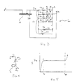
- Fig. 3 illustrates one embodiment of the invention provided herein.
- a current limiter 2 is provided with a transistor 10 which in a preferred embodiment is a field effect transistor of the type commonly known to those of skill in the art.
- the transistor 10 is a depletion mode transistor, i.e., a transistor in which there is a conducting channel between the source and the drain when the gate and source are at the same potential. While an n-channel device is shown in Fig. 3, it will be readily apparent upon review of this disclosure that current limiters based on p-channel devices could also be fabricated. Also, while a two-pin device is illustrated in Fig. 3, a three-pin device could also be readily fabricated based upon this disclosure.
- the source of the depletion mode transistor 10 is connected to a parallel network of shunt resistors 12.
- the parallel network of shunt resistors 12 includes a first group of resistors 14a, 14b, 14c, and 14d.
- the network may also include a second group of fixed transistors 16a and 16b. It is preferred to provide optional resistors 16 so the device will provide a limit on current event if all the fusible links are blown.
- the gate of the depletion mode transistor is connected to the output of the network 12.
- Each of the first group of resistors is provided with a series fusible link 18a, 18b, 18c, and 18d while the optional resistors 16a and 16b are not provided with such a link.
- the invention is illustrated herein with 4 fused transistors and 2 fixed transistors, but of course a wide variety of arrangements could be provided. In general it is desirable to provide 2 or more fused resistors in the network and 1 or more fixed transistors. The selection of the number of resistors provided in the network will be based on the range of current values which the current limiter is intended to cover. Also, while the invention is illustrated herein with regard to discrete transistors 14 and 16, it will be recognized that each of these discrete transistors could actually include one or more resistors or other load devices in series or parallel.
- the value of resistance to be supplied for each resistor will also vary widely depending upon the application.
- the resistance values may range from about 10 ohms to 100,000 ohms or more in some applications. More particularly, resistance values may range from about 100 ohms to 10,000 ohms in some applications. Still more particularly, resistance values may range from about 200 ohms to 8,000 ohms in typical applications. These values are meant to be illustrative and in no way limiting on the resistance values used in actual applications.
- the resistors When it is desirable to mass-produce current limiters, all of which provide a nearly identical output, the resistors will be used to account for variations in the fabrication of the device as a result of changing process conditions and the like. In this situation, the values of resistance provided by at least several of the resistors will be closely spaced. For example, resistances varying by between about 10% and 1000% would be used in some embodiments with resistances varying between about 50% and 100% preferred. Of course, the invention will find other applications. For example, the invention may be utilized to fabricate current limiters which may be used to provide widely varying current outputs. In this case, the resistance of the various resistors could vary by 1000% or more.
- the resistor network 12 is used to vary the output current by selectively blowing one or more of the fuses.
- the fuses are blown by applying an appropriate voltage across the fusible links via on-chip trimming pads or pins P1, P2, P3, and/or P4, and the ground pad or pin P g .
- the output of the current limiter may be precisely adjusted in the fab during a wafer testing operation.
- the customer would, in some embodiments, selectively blow fuses in sequence until the desired current is output.
- fuses may be blown with lasers, ultrasonic pulses, or the like.
- Fig. 4 provides an illustration of the device 2 in a two-pin configuration.
- the device is connected to a source of variable voltage 20, but provides a constant current I d .
- the output characteristics of the device are illustrated in Fig. 5. As shown, the device output reaches I D at V min , after which its output is largely independent of applied voltage up to a breakdown voltage V bd .
- V min is typically 3-4 volts while V bd is 100 to 1200 volts.
- the device discussed above may be produced by way of a large variety of fabrication sequences.
- the device may, for example, be fabricated according to the method described in U.S. Patent No. 4,860,072, which is incorporated herein by reference for all purposes.
- the device is fabricated by way of a process in which resistors for the resistance network may be fabricated without additional masking steps.
- polysilicon resistors are utilized and the same polysilicon that is used for the gate is used for the resistor network such as in, for example, U.S. Patent No. 4,764,480, which is incorporated herein by reference for all purposes.
- the preferred resistor is a p-well resistor (for the n-channel device), since the temperature coefficient of the resistor compensates and cancels the effect of the temperature on the gain of the FET thus keeping the current level constant to a high degree with temperature.
Landscapes
- Engineering & Computer Science (AREA)
- Power Engineering (AREA)
- Control Of Electrical Variables (AREA)
- Semiconductor Integrated Circuits (AREA)
Applications Claiming Priority (2)
| Application Number | Priority Date | Filing Date | Title |
|---|---|---|---|
| US494198 | 1983-05-13 | ||
| US07/494,198 US5191279A (en) | 1990-03-15 | 1990-03-15 | Current limiting method and apparatus |
Publications (3)
| Publication Number | Publication Date |
|---|---|
| EP0446724A2 true EP0446724A2 (de) | 1991-09-18 |
| EP0446724A3 EP0446724A3 (en) | 1992-07-29 |
| EP0446724B1 EP0446724B1 (de) | 1996-07-31 |
Family
ID=23963462
Family Applications (1)
| Application Number | Title | Priority Date | Filing Date |
|---|---|---|---|
| EP91103101A Expired - Lifetime EP0446724B1 (de) | 1990-03-15 | 1991-03-01 | Verfahren und Vorrichtung zur Strombegrenzung |
Country Status (4)
| Country | Link |
|---|---|
| US (1) | US5191279A (de) |
| EP (1) | EP0446724B1 (de) |
| JP (1) | JPH05173655A (de) |
| DE (1) | DE69121124T2 (de) |
Cited By (3)
| Publication number | Priority date | Publication date | Assignee | Title |
|---|---|---|---|---|
| EP0593588B1 (de) * | 1991-07-08 | 1997-03-26 | Raychem Limited | Schutzeinrichtung für schaltung |
| WO2009014765A1 (en) * | 2007-07-26 | 2009-01-29 | Fultec Semiconductor, Inc. | Transient blocking unit having a fab-adjustable threshold current |
| WO2010050917A1 (en) * | 2008-10-31 | 2010-05-06 | Moog Inc. | Power supplies with testable current limiters, and methods of operating same |
Families Citing this family (11)
| Publication number | Priority date | Publication date | Assignee | Title |
|---|---|---|---|---|
| FR2705173B1 (fr) * | 1993-05-10 | 1995-07-28 | Sgs Thomson Microelectronics | Composant limiteur de courant serie. |
| DE4333065A1 (de) * | 1993-09-29 | 1995-03-30 | Bosch Gmbh Robert | Elektronische Schaltung |
| US5629536A (en) * | 1995-11-21 | 1997-05-13 | Motorola, Inc. | High voltage current limiter and method for making |
| US6054847A (en) * | 1998-09-09 | 2000-04-25 | International Business Machines Corp. | Method and apparatus to automatically select operating voltages for a device |
| US20050062584A1 (en) * | 2003-09-24 | 2005-03-24 | Broadcom Corporation | High-linearity switched-resistor network for programmability |
| EP1727203A1 (de) * | 2005-05-24 | 2006-11-29 | STMicroelectronics S.r.l. | Monolithisch integrierte Leistungs-IGBT Vorrichtung (Bipolartransistor mit isolierter Gate-Elektrode) |
| TW200727588A (en) * | 2006-01-11 | 2007-07-16 | Richtek Techohnology Corp | Voltage-supply apparatus and control method thereof |
| US8050005B2 (en) * | 2006-12-20 | 2011-11-01 | Telefonaktiebolaget Lm Ericsson | Automatic function with selectable fuse rating for single fuses and fuse panels |
| US20100016034A1 (en) * | 2008-06-10 | 2010-01-21 | Telefonaktiebolaget L M Ericsson (Publ) | Power supply method and apparatus for radio access network nodes/sites |
| US10205313B2 (en) | 2015-07-24 | 2019-02-12 | Symptote Technologies, LLC | Two-transistor devices for protecting circuits from sustained overcurrent |
| CN108292837B (zh) | 2015-09-21 | 2020-01-17 | 西普托特技术有限责任公司 | 用于保护电路的单晶体管器件以及方法 |
Family Cites Families (13)
| Publication number | Priority date | Publication date | Assignee | Title |
|---|---|---|---|---|
| US4016483A (en) * | 1974-06-27 | 1977-04-05 | Rudin Marvin B | Microminiature integrated circuit impedance device including weighted elements and contactless switching means for fixing the impedance at a preselected value |
| JPS5450948A (en) * | 1977-09-30 | 1979-04-21 | Toshiba Corp | Bidirectional constant current circuit |
| JPS56132815A (en) * | 1980-03-21 | 1981-10-17 | Nec Corp | Reference step voltage generating circuit |
| JPS5787224A (en) * | 1980-11-18 | 1982-05-31 | Toyoda Mach Works Ltd | Linearizer |
| US4412241A (en) * | 1980-11-21 | 1983-10-25 | National Semiconductor Corporation | Multiple trim structure |
| US4862136A (en) * | 1983-04-13 | 1989-08-29 | Birkner John M | Programmable resistance network |
| US4713599A (en) * | 1985-01-04 | 1987-12-15 | Motorola, Inc. | Programmable trimmable circuit having voltage limiting |
| US4766366A (en) * | 1985-01-04 | 1988-08-23 | Motorola, Inc. | Trimmable current source |
| FR2582150B1 (fr) * | 1985-05-15 | 1987-10-23 | Cahen Olivier | Dispositif de compensation des ecarts de tension de seuil des transistors a effet de champ des circuits integres analogiques |
| US4860072A (en) * | 1986-03-05 | 1989-08-22 | Ixys Corporation | Monolithic semiconductor device and method of manufacturing same |
| US4788620A (en) * | 1987-11-09 | 1988-11-29 | General Electric Company | Static trip circuit breaker with automatic circuit trimming |
| US4978904A (en) * | 1987-12-15 | 1990-12-18 | Gazelle Microcircuits, Inc. | Circuit for generating reference voltage and reference current |
| US4868416A (en) * | 1987-12-15 | 1989-09-19 | Gazelle Microcircuits, Inc. | FET constant reference voltage generator |
-
1990
- 1990-03-15 US US07/494,198 patent/US5191279A/en not_active Expired - Lifetime
-
1991
- 1991-03-01 EP EP91103101A patent/EP0446724B1/de not_active Expired - Lifetime
- 1991-03-01 DE DE69121124T patent/DE69121124T2/de not_active Expired - Lifetime
- 1991-03-15 JP JP3074313A patent/JPH05173655A/ja active Pending
Cited By (4)
| Publication number | Priority date | Publication date | Assignee | Title |
|---|---|---|---|---|
| EP0593588B1 (de) * | 1991-07-08 | 1997-03-26 | Raychem Limited | Schutzeinrichtung für schaltung |
| WO2009014765A1 (en) * | 2007-07-26 | 2009-01-29 | Fultec Semiconductor, Inc. | Transient blocking unit having a fab-adjustable threshold current |
| GB2463626A (en) * | 2007-07-26 | 2010-03-24 | Fultec Semiconductor Inc | Transient blocking unit having a fab-adjustable threshold current |
| WO2010050917A1 (en) * | 2008-10-31 | 2010-05-06 | Moog Inc. | Power supplies with testable current limiters, and methods of operating same |
Also Published As
| Publication number | Publication date |
|---|---|
| DE69121124T2 (de) | 1996-12-12 |
| US5191279A (en) | 1993-03-02 |
| DE69121124D1 (de) | 1996-09-05 |
| EP0446724A3 (en) | 1992-07-29 |
| EP0446724B1 (de) | 1996-07-31 |
| JPH05173655A (ja) | 1993-07-13 |
Similar Documents
| Publication | Publication Date | Title |
|---|---|---|
| US5191279A (en) | Current limiting method and apparatus | |
| US6836144B1 (en) | Programmable series on-chip termination impedance and impedance matching | |
| US7019585B1 (en) | Method and circuit for adjusting a reference voltage signal | |
| EP0225441B1 (de) | Programmierstrom-Steuergerät | |
| US6807040B2 (en) | Over-current protection circuit and method | |
| EP0410595B1 (de) | Abgleichschaltungen | |
| US20010052790A1 (en) | On-chip substrate regulator test mode | |
| EP0782193A1 (de) | Selbstanpassende Widerstandsabgleichschaltung | |
| EP0674389B1 (de) | Überlastschutzschaltkreis für MOS-Leistungstreiber | |
| US6664814B1 (en) | Output driver for an integrated circuit | |
| EP0760555A1 (de) | Strom-Generatorschaltung mit einem breiten Frequenzgang | |
| JPH0949858A (ja) | 電流検出制御回路及びパターンレイアウト方法 | |
| KR100904111B1 (ko) | 전압 제어 회로 | |
| US20090027822A1 (en) | Transient blocking unit having a fab-adjustable threshold current | |
| US20070171589A1 (en) | Zapping Circuit | |
| US5914626A (en) | Voltage clamping circuit for semiconductor devices | |
| US10379565B2 (en) | Output driver circuit | |
| JPH0648598B2 (ja) | 集積回路用内部高電圧(Vpp)レギュレータ | |
| JPH05275999A (ja) | パワーデバイスの駆動保護回路 | |
| US5939934A (en) | Integrated circuit passively biasing transistor effective threshold voltage and related methods | |
| US11012041B2 (en) | Differential amplifier circuit | |
| US7463012B2 (en) | Bandgap reference circuits with isolated trim elements | |
| US6476667B1 (en) | Adjustable current limiting/sensing circuitry and method | |
| US20010050576A1 (en) | On-chip substrate regulator test mode | |
| US20030098740A1 (en) | MOS-based voltage reference circuit |
Legal Events
| Date | Code | Title | Description |
|---|---|---|---|
| PUAI | Public reference made under article 153(3) epc to a published international application that has entered the european phase |
Free format text: ORIGINAL CODE: 0009012 |
|
| AK | Designated contracting states |
Kind code of ref document: A2 Designated state(s): DE FR GB |
|
| PUAL | Search report despatched |
Free format text: ORIGINAL CODE: 0009013 |
|
| AK | Designated contracting states |
Kind code of ref document: A3 Designated state(s): DE FR GB |
|
| 17P | Request for examination filed |
Effective date: 19930108 |
|
| 17Q | First examination report despatched |
Effective date: 19941128 |
|
| GRAH | Despatch of communication of intention to grant a patent |
Free format text: ORIGINAL CODE: EPIDOS IGRA |
|
| GRAH | Despatch of communication of intention to grant a patent |
Free format text: ORIGINAL CODE: EPIDOS IGRA |
|
| GRAA | (expected) grant |
Free format text: ORIGINAL CODE: 0009210 |
|
| AK | Designated contracting states |
Kind code of ref document: B1 Designated state(s): DE FR GB |
|
| PG25 | Lapsed in a contracting state [announced via postgrant information from national office to epo] |
Ref country code: FR Effective date: 19960731 |
|
| REF | Corresponds to: |
Ref document number: 69121124 Country of ref document: DE Date of ref document: 19960905 |
|
| EN | Fr: translation not filed | ||
| PLBE | No opposition filed within time limit |
Free format text: ORIGINAL CODE: 0009261 |
|
| STAA | Information on the status of an ep patent application or granted ep patent |
Free format text: STATUS: NO OPPOSITION FILED WITHIN TIME LIMIT |
|
| 26N | No opposition filed | ||
| REG | Reference to a national code |
Ref country code: GB Ref legal event code: IF02 |
|
| PGFP | Annual fee paid to national office [announced via postgrant information from national office to epo] |
Ref country code: GB Payment date: 20100219 Year of fee payment: 20 |
|
| PGFP | Annual fee paid to national office [announced via postgrant information from national office to epo] |
Ref country code: DE Payment date: 20100331 Year of fee payment: 20 |
|
| REG | Reference to a national code |
Ref country code: DE Ref legal event code: R071 Ref document number: 69121124 Country of ref document: DE |
|
| REG | Reference to a national code |
Ref country code: GB Ref legal event code: PE20 Expiry date: 20110228 |
|
| PG25 | Lapsed in a contracting state [announced via postgrant information from national office to epo] |
Ref country code: GB Free format text: LAPSE BECAUSE OF EXPIRATION OF PROTECTION Effective date: 20110228 |
|
| PG25 | Lapsed in a contracting state [announced via postgrant information from national office to epo] |
Ref country code: DE Free format text: LAPSE BECAUSE OF EXPIRATION OF PROTECTION Effective date: 20110301 |