EP0446549B1 - Verfahren für das Messen der Dimensionen eines Abstandshalters - Google Patents
Verfahren für das Messen der Dimensionen eines Abstandshalters Download PDFInfo
- Publication number
- EP0446549B1 EP0446549B1 EP90420552A EP90420552A EP0446549B1 EP 0446549 B1 EP0446549 B1 EP 0446549B1 EP 90420552 A EP90420552 A EP 90420552A EP 90420552 A EP90420552 A EP 90420552A EP 0446549 B1 EP0446549 B1 EP 0446549B1
- Authority
- EP
- European Patent Office
- Prior art keywords
- spacer
- spacers
- lobe
- substrate
- dimensions
- Prior art date
- Legal status (The legal status is an assumption and is not a legal conclusion. Google has not performed a legal analysis and makes no representation as to the accuracy of the status listed.)
- Expired - Lifetime
Links
- 125000006850 spacer group Chemical group 0.000 title claims abstract description 80
- 238000000034 method Methods 0.000 title claims abstract description 18
- 239000000758 substrate Substances 0.000 claims abstract description 17
- 238000004519 manufacturing process Methods 0.000 claims description 14
- 230000001747 exhibiting effect Effects 0.000 claims 1
- 238000005530 etching Methods 0.000 description 37
- 238000005259 measurement Methods 0.000 description 10
- 239000000463 material Substances 0.000 description 9
- 235000012431 wafers Nutrition 0.000 description 6
- 230000008901 benefit Effects 0.000 description 3
- 238000000151 deposition Methods 0.000 description 2
- 230000001066 destructive effect Effects 0.000 description 2
- 238000001514 detection method Methods 0.000 description 2
- 238000012886 linear function Methods 0.000 description 2
- 238000000206 photolithography Methods 0.000 description 2
- 240000008042 Zea mays Species 0.000 description 1
- 239000011324 bead Substances 0.000 description 1
- 238000004364 calculation method Methods 0.000 description 1
- 238000011088 calibration curve Methods 0.000 description 1
- 238000005229 chemical vapour deposition Methods 0.000 description 1
- 230000007423 decrease Effects 0.000 description 1
- 230000008021 deposition Effects 0.000 description 1
- 238000010586 diagram Methods 0.000 description 1
- 238000001493 electron microscopy Methods 0.000 description 1
- 230000008030 elimination Effects 0.000 description 1
- 238000003379 elimination reaction Methods 0.000 description 1
- 238000011065 in-situ storage Methods 0.000 description 1
- 230000000873 masking effect Effects 0.000 description 1
- 238000000691 measurement method Methods 0.000 description 1
- 238000004377 microelectronic Methods 0.000 description 1
- 238000003908 quality control method Methods 0.000 description 1
- 239000004065 semiconductor Substances 0.000 description 1
- 229910021332 silicide Inorganic materials 0.000 description 1
- FVBUAEGBCNSCDD-UHFFFAOYSA-N silicide(4-) Chemical compound [Si-4] FVBUAEGBCNSCDD-UHFFFAOYSA-N 0.000 description 1
- 238000004088 simulation Methods 0.000 description 1
- 238000005507 spraying Methods 0.000 description 1
- 230000001052 transient effect Effects 0.000 description 1
Images

Classifications
-
- G—PHYSICS
- G01—MEASURING; TESTING
- G01B—MEASURING LENGTH, THICKNESS OR SIMILAR LINEAR DIMENSIONS; MEASURING ANGLES; MEASURING AREAS; MEASURING IRREGULARITIES OF SURFACES OR CONTOURS
- G01B11/00—Measuring arrangements characterised by the use of optical techniques
- G01B11/02—Measuring arrangements characterised by the use of optical techniques for measuring length, width or thickness
- G01B11/06—Measuring arrangements characterised by the use of optical techniques for measuring length, width or thickness for measuring thickness ; e.g. of sheet material
- G01B11/0616—Measuring arrangements characterised by the use of optical techniques for measuring length, width or thickness for measuring thickness ; e.g. of sheet material of coating
- G01B11/0675—Measuring arrangements characterised by the use of optical techniques for measuring length, width or thickness for measuring thickness ; e.g. of sheet material of coating using interferometry
-
- G—PHYSICS
- G01—MEASURING; TESTING
- G01B—MEASURING LENGTH, THICKNESS OR SIMILAR LINEAR DIMENSIONS; MEASURING ANGLES; MEASURING AREAS; MEASURING IRREGULARITIES OF SURFACES OR CONTOURS
- G01B11/00—Measuring arrangements characterised by the use of optical techniques
- G01B11/02—Measuring arrangements characterised by the use of optical techniques for measuring length, width or thickness
- G01B11/024—Measuring arrangements characterised by the use of optical techniques for measuring length, width or thickness by means of diode-array scanning
Definitions
- the present invention relates to a method for measuring the characteristic dimensions of a spacer or similar structure used in particular during the manufacture of certain integrated circuits.
- the present invention applies in particular to the field of integrated circuits where it is useful for certain quality control operations during manufacture.
- spacers In the production of certain integrated circuits, it is necessary to constitute particular structures which are called spacers.
- a spacer consists of a residue of a certain material, located exclusively against the vertical lateral edges of the structures present at the time of the step of making the spacer.
- a layer of uniform thickness of a certain material is deposited on the wafer during treatment, then an anisotropic etching of this layer is carried out.
- the etching operation of this layer is stopped as soon as the areas of this layer located on horizontal or inclined parts of the underlying structures are completely removed. Under these conditions, the parts of this layer located, very locally, against the vertical lateral edges of the underlying structures are only partially etched and therefore leave locally a bead of very small width which constitutes the spacer.
- This technique essentially has the advantage of being able to produce certain microstructures in a self-aligned manner, without masking and photolithography.
- LDD Lightly Doped Drain
- a known method for controlling the shape and dimensions of the spacers is to break a wafer transversely to the spacers and examine the cross section through an electron microscope. This method is expensive, time consuming and delicate. In addition, it is destructive. To date, no reliable, non-destructive and immediate control method for spacers is known.
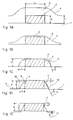
- FIG. 1 schematically illustrates the structure which must be produced before the etching operation intended for the production of the spacers.
- a layer of a first material is deposited, over a thickness e.
- An operation, known per se, is then carried out of photolithography and anisotropic etching leading to the production, from the initially deposited layer, of patterns 2 having a rectangular cross section.
- a layer 3 of a second material is then deposited on the entire wafer over a thickness f.
- Layer 3 can be deposited by spraying or by a chemical vapor deposition process.
- the upper surface 4 of the layer 3 is horizontal in the zones situated on the underlying zones which are themselves horizontal and is clearly inclined in the transient zones corresponding to a step change.
- FIG. 1C represents this etching stage during which the spacers 7 are produced.
- the inhomogeneities of deposition and etching can be compensated for by continuing the etching operation up to the stage shown in FIG. 1D. If etching is continued, a thinning of the spacer 7 is obtained, its height h is significantly reduced and its width l is also reduced, as shown in FIG. 1E. By continuing the etching even more, it is possible to obtain the total elimination of the spacer 7 (not shown). It should be noted that this further etching is accompanied by the consumption of the substrate 1.
- the difficulty in producing the spacers lies in the fact that the etching operation must be stopped at a precise moment in order to obtain a spacer of the desired shape (as shown in FIG. 1D).
- many other factors are likely to create disparities in the constitution of the spacers 7. Indeed, if the initial thickness f of the layer 3 is slightly too large or too small, the spacer 7 which will result therefrom the engraving operation will not be in conformity. If, moreover, the material constituting the layer 3 has characteristics slightly different from those considered to be normal, it may cause a higher or lower etching speed, also leading to the production of non-conforming spacers 7.
- the actual etching process can also be subject to unwanted variations resulting from certain misadjustments of machines or equipment.
- the invention as will be seen in the detailed description which follows, makes it possible to meet these wishes.
- the cross section of the spacer 7 has a general shape approaching a triangle whose side opposite the right angle is slightly curved. This characteristic is not essential for understanding the object of the present invention. Moreover, in certain methods of producing spacers these may have slightly different shapes.
- the height h of the spacer 7 corresponds to the distance separating the upper edge 8 of the spacer, in contact with the vertical lateral edge 6 of the pattern 2, and the planar upper surface 9 of the substrate 1;
- the width l is equal to the distance separating the lateral edge 6 of the pattern 2, at its contact with the substrate 1, and the outer edge 10 of the spacer 7, at its contact with the substrate 1;
- the angle ⁇ is the angle that the tangent 11 forms at the outer edge 10 of the spacer, at its contact with the substrate 1.
- FIGS. 2, 3 and 4 Reference will now be made essentially to FIGS. 2, 3 and 4 to describe in more detail the measurement method according to the present invention.
- FIGS. 1A to 1E represent either microstructures of integrated circuits with which it is desired to associate spacers 7 or else parallel strips forming a network to which it is also envisaged to associate spacers 7 intended for dimensional control.
- spacers are then produced on the lateral edges 6 of the parallel strips 2.
- the steps described in relation to FIG. 1 are carried out.
- the network 2 is illuminated with a monochromatic light beam.
- the light diffracted by the grating produces a diffraction pattern composed of a main light spot 15 corresponding to the specular reflection and of a multitude of adjacent aligned diffraction spots whose envelope has a lobe main L0 including the main spot 15 and secondary lobes among which the first lobe L1 is adjacent to the main lobe L0.
- the present invention measures the light intensity of spots constituting the first lobe L1.
- a group of spots of the lobe L1 will preferably be selected, the light intensity of which varies notably with the degree of etching of the spacer.
- the present invention is based on the observation made by the applicant that one can deduce this measurement of light intensity IL1 from one or more spots of the first lobe L1, the width l, the angle ⁇ and the difference in height. d, by comparison with calibration curves.
- the light intensity IL1 of the first lobe L1 is in linear relationship, both with the width l of the spacer 7, the angle ⁇ of the spacer 7 and the difference in height d when the latter is negative, that is to say when the height h of the spacer 7 is less than the thickness e of the parallel strips 2.
- FIG. 3 represents the linear relationship between the measurement of light intensity IL1 and the width l of the spacer.
- the light intensity of the lobe L1 increases when the width l of the spacer 7 decreases.
- We can therefore easily, by a set of preliminary experimental measurements or by a simulation, determine the linear function connecting l and IL1 by a function of the type: l k1 ⁇ IL1 + k2 in which k1 and k2 are two constants.
- FIG. 4 represents the linear relationship between the parameter IL1 and ⁇ .
- ⁇ k3 ⁇ IL1 + k4, in which k3 and k4 are two constants.
- FIG. 5 represents the evolution of the algebraic value d during the etching operation as a function of the light intensity of a determined group of spots belonging to the first lobe 1.
- the very beginning of the etching operation corresponds to FIG. 1A.
- the mark B in FIG. 5 corresponds to the etching level of FIG. 1B, and so on for the marks C, D and E.
- the marks C, D and E correspond respectively to the level of etching shown in Figures 1C, 1D and 1E.
- the light intensity IL1 has increased to that the etching reaches the state shown in Figure 1C, that is to say when the horizontal areas of the layer 3 are completely removed.
- the states represented in FIGS. 1D and 1E it can be seen that the light intensity IL1 has evolved linearly as a function of the algebraic value d.
- the invention can be easily implemented using an appropriate device (not shown).
- This device essentially comprises a monochromatic light source, generally a laser source, which strikes at a determined angle of incidence, the network of parallel bands.
- the apparatus also comprises a detector which is situated at the level of the diffraction spots and which may consist, for example, of a strip of CCD sensors.
- the apparatus then comprises, in a manner known per se, a set of electronic devices making it possible to locate the different light spots, to spot the spot 15 corresponding to the specular reflection, to count the different spots and to spot the first lobe L1 and, in this lobe L1, the brightest spot 16.
- the device can then carry out the intensity measurements IL1 corresponding to the process previously described and carry out very simple calculations to directly edit the values of the parameters l, ⁇ and d.
Landscapes
- Physics & Mathematics (AREA)
- General Physics & Mathematics (AREA)
- Length Measuring Devices By Optical Means (AREA)
- Length Measuring Devices With Unspecified Measuring Means (AREA)
Claims (2)
- Verfahren zum Messen der Dimensionen eines Abstandshalters mit folgenden Merkmalen:- Ausbilden eines Netzes paralleler Streifen (2) auf einem Substrat (1), wobei jeder Streifen (2) einen rechteckigen Querschnitt aufweist;- Ausbilden von Abstandshaltern (7) an den Seitenrändern (6) der parallelen Streifen (2), wobei diese Abstandshalter eine Breite l entsprechend der Entfernung zwischen dem Rand (6) des Streifens (2) und dem äußeren Rand (10) des Abstandshalters (7) auf dem Niveau der jeweiligen Berührungspunkte mit dem Substrat und einen Winkel ϑ zwischen der Ebene des Substrats und der Tangente (11) an den äußeren Rand des Abstandshalters auf dem Niveau des Substrats aufweisen;- im Verlauf des Ausbildens der Abstandshalter oder anschließend hieran Beleuchten des Netzes durch ein monochromatisches Lichtbündel, dessen gestreutes Licht eine Streufigur erzeugt, die aus einem leuchtenden Hauptpunkt (15) entsprechend der direkten Spiegelreflexion und einer Vielzahl längs einer Linie ausgerichteter benachbarter Streupunkte zusammengesetzt ist, wobei die Einhüllende eine Hauptkurve (LO), die den Hauptpunkt (15) einschließt, und Nebenkurven bildet, von denen die erste Nebenkurve (L1) der Hauptkurve (LO) benachbart liegt;- Messen der Summe der Lichtintensitäten (IL1) einer vorbestimmten Anzahl von Punkten, die der Hauptkurve (L1) zugehörig sind; und- Ableiten daraus der Breite l und des Winkels ϑ des Abstandshalters (7) durch die folgenden Formeln:


- Verfahren zum Messen der Dimensionen eines Abstandshalters nach Anspruch 1, wobei der Abstandshalter zudem eine Höhe h aufweist, die, in einem Querschnitt, der Entfernung zwischen dem oberen Rand (8) des Abstandshalters am Berührungspunkt mit dem Seitenrand (6) des parallelen Streifens (2) und der Oberfläche (9) des Substrats (1) entspricht, und wobei ein algebraischer Wert d der Differenz zwischen der Höhe h und der Dicke e des parallelen Streifens (2) entspricht, dadurch gekennzeichnet, daß der algebraische Wert d durch die folgende Formel abgeleitet wird:

Priority Applications (1)
| Application Number | Priority Date | Filing Date | Title |
|---|---|---|---|
| AT90420552T ATE104428T1 (de) | 1989-12-21 | 1990-12-18 | Verfahren fuer das messen der dimensionen eines abstandshalters. |
Applications Claiming Priority (2)
| Application Number | Priority Date | Filing Date | Title |
|---|---|---|---|
| FR8917387 | 1989-12-21 | ||
| FR8917387A FR2656465B1 (fr) | 1989-12-21 | 1989-12-21 | Procede de mesure des dimensions d'un espaceur. |
Publications (3)
| Publication Number | Publication Date |
|---|---|
| EP0446549A2 EP0446549A2 (de) | 1991-09-18 |
| EP0446549A3 EP0446549A3 (de) | 1991-09-25 |
| EP0446549B1 true EP0446549B1 (de) | 1994-04-13 |
Family
ID=9389103
Family Applications (1)
| Application Number | Title | Priority Date | Filing Date |
|---|---|---|---|
| EP90420552A Expired - Lifetime EP0446549B1 (de) | 1989-12-21 | 1990-12-18 | Verfahren für das Messen der Dimensionen eines Abstandshalters |
Country Status (6)
| Country | Link |
|---|---|
| US (1) | US5103104A (de) |
| EP (1) | EP0446549B1 (de) |
| JP (1) | JP2857495B2 (de) |
| AT (1) | ATE104428T1 (de) |
| DE (1) | DE69008156T2 (de) |
| FR (1) | FR2656465B1 (de) |
Families Citing this family (9)
| Publication number | Priority date | Publication date | Assignee | Title |
|---|---|---|---|---|
| US5805290A (en) * | 1996-05-02 | 1998-09-08 | International Business Machines Corporation | Method of optical metrology of unresolved pattern arrays |
| US5965309A (en) * | 1997-08-28 | 1999-10-12 | International Business Machines Corporation | Focus or exposure dose parameter control system using tone reversing patterns |
| US5976740A (en) * | 1997-08-28 | 1999-11-02 | International Business Machines Corporation | Process for controlling exposure dose or focus parameters using tone reversing pattern |
| US5953128A (en) * | 1997-08-28 | 1999-09-14 | International Business Machines Corporation | Optically measurable serpentine edge tone reversed targets |
| US5914784A (en) * | 1997-09-30 | 1999-06-22 | International Business Machines Corporation | Measurement method for linewidth metrology |
| US6137578A (en) * | 1998-07-28 | 2000-10-24 | International Business Machines Corporation | Segmented bar-in-bar target |
| US6128089A (en) * | 1998-07-28 | 2000-10-03 | International Business Machines Corporation | Combined segmented and nonsegmented bar-in-bar targets |
| GB2340980A (en) * | 1998-08-21 | 2000-03-01 | Ezio Panzeri | A coded token |
| US7400417B2 (en) * | 2005-05-23 | 2008-07-15 | Federal Mogul World Wide, Inc. | Diffraction method for measuring thickness of a workpart |
Family Cites Families (8)
| Publication number | Priority date | Publication date | Assignee | Title |
|---|---|---|---|---|
| JPS56120904A (en) * | 1980-02-29 | 1981-09-22 | Chugoku Toryo Kk | Measuring method for rate of removal of coating film |
| JPS60196605A (ja) * | 1984-03-19 | 1985-10-05 | Nippon Kogaku Kk <Nikon> | 散乱光検出光学装置 |
| US4842411A (en) * | 1986-02-06 | 1989-06-27 | Vectron, Inc. | Method of automatically measuring the shape of a continuous surface |
| JPH07122574B2 (ja) * | 1986-07-25 | 1995-12-25 | 株式会社日立製作所 | 断面形状測定方法 |
| JPS63147327A (ja) * | 1986-12-10 | 1988-06-20 | Dainippon Screen Mfg Co Ltd | 表面処理における処理終点検知方法 |
| US4846920A (en) * | 1987-12-09 | 1989-07-11 | International Business Machine Corporation | Plasma amplified photoelectron process endpoint detection apparatus |
| JP2542653B2 (ja) * | 1987-12-10 | 1996-10-09 | ファナック株式会社 | 非接触倣い方法 |
| US5024949A (en) * | 1989-02-17 | 1991-06-18 | Biotrol, Inc. | Aerobic bacterial remediation of aliphatic chlorinated hydrocarbon contamination |
-
1989
- 1989-12-21 FR FR8917387A patent/FR2656465B1/fr not_active Expired - Lifetime
-
1990
- 1990-12-18 DE DE69008156T patent/DE69008156T2/de not_active Expired - Fee Related
- 1990-12-18 AT AT90420552T patent/ATE104428T1/de not_active IP Right Cessation
- 1990-12-18 EP EP90420552A patent/EP0446549B1/de not_active Expired - Lifetime
- 1990-12-20 JP JP2404108A patent/JP2857495B2/ja not_active Expired - Lifetime
- 1990-12-20 US US07/631,733 patent/US5103104A/en not_active Expired - Lifetime
Also Published As
| Publication number | Publication date |
|---|---|
| DE69008156T2 (de) | 1994-12-01 |
| US5103104A (en) | 1992-04-07 |
| EP0446549A3 (de) | 1991-09-25 |
| DE69008156D1 (de) | 1994-05-19 |
| FR2656465B1 (fr) | 1992-05-07 |
| ATE104428T1 (de) | 1994-04-15 |
| EP0446549A2 (de) | 1991-09-18 |
| JP2857495B2 (ja) | 1999-02-17 |
| FR2656465A1 (fr) | 1991-06-28 |
| JPH06180210A (ja) | 1994-06-28 |
Similar Documents
| Publication | Publication Date | Title |
|---|---|---|
| EP0446549B1 (de) | Verfahren für das Messen der Dimensionen eines Abstandshalters | |
| WO2009138835A1 (fr) | Procede de controle en temps reel de la fabrication de circuits integres a l'aide de structures de controle localisees dans l'espace modele opc | |
| FR2951543A1 (fr) | Procede d'analyse de la qualite d'un vitrage | |
| US20150042988A1 (en) | Sers-sensor with nanostructured surface and methods of making and using | |
| EP0294873A1 (de) | Testvorrichtung zur Durchführung eines Realisierungsverfahrens von Halbleiterstrukturen | |
| EP1439580B1 (de) | Herstellung feiner und dicht angeordneter Gräben | |
| FR3083644A1 (fr) | Capteur d'images | |
| CA2457899C (fr) | Capteur d'image couleur sur substrat transparent et procede de fabrication | |
| EP3355118B1 (de) | Verfahren zum messen des versatzes zwischen einer ersten und einer zweiten gravurzone | |
| FR2548450A1 (fr) | Procede de fabrication de diode en film mince ultra-miniature | |
| EP0262055B1 (de) | Messverfahren für das Fliessen eines Materials | |
| EP2495754A2 (de) | Herstellungsverfahren eines integrierten Schaltkreises, das auf der Bildung von Leitungen und Gräben beruht | |
| EP0378033A1 (de) | Einstellungsverfahren für eine photolithographische Belichtungsvorrichtung | |
| EP0274966B1 (de) | Verfahren zur quantitativen Reliefsermittlung eines Motivs sehr kleiner Abmessungen | |
| EP0413645B1 (de) | Verfahren zum Herstellen eines Mesa-MOS-Transistors des Typs SOI | |
| CN117316793B (zh) | 一种外延片表面台阶检测方法及装置 | |
| FR2754905A1 (fr) | Procede de realisation d'un capteur magnetique magnetoresistif et capteur obtenu par ce procede | |
| US20070172977A1 (en) | Methods for forming alignment marks on semiconductor devices | |
| JP3003642B2 (ja) | 異物検出感度校正用標準サンプル及びその製造方法 | |
| EP0493269B1 (de) | Verfahren zur Messung der Viskosität eines Materials | |
| WO2007004177A2 (en) | Method of measuring deep trenches with model-based optical spectroscopy | |
| KR100980257B1 (ko) | 액정표시소자용 박막 트랜지스터 패턴 깊이 측정장치 및 측정방법 | |
| WO2012143649A1 (fr) | Procede d'analyse de la qualite d'un vitrage | |
| FR2880987A1 (fr) | Procede de gravure d'une galette en matiere cristalline | |
| JPH0634806A (ja) | ダマングレーティングの製作方法 |
Legal Events
| Date | Code | Title | Description |
|---|---|---|---|
| PUAI | Public reference made under article 153(3) epc to a published international application that has entered the european phase |
Free format text: ORIGINAL CODE: 0009012 |
|
| PUAL | Search report despatched |
Free format text: ORIGINAL CODE: 0009013 |
|
| AK | Designated contracting states |
Kind code of ref document: A2 Designated state(s): AT DE FR GB IT NL |
|
| AK | Designated contracting states |
Kind code of ref document: A3 Designated state(s): AT DE FR GB IT NL |
|
| 17P | Request for examination filed |
Effective date: 19920220 |
|
| 17Q | First examination report despatched |
Effective date: 19930302 |
|
| RAP1 | Party data changed (applicant data changed or rights of an application transferred) |
Owner name: FRANCE TELECOM |
|
| GRAA | (expected) grant |
Free format text: ORIGINAL CODE: 0009210 |
|
| AK | Designated contracting states |
Kind code of ref document: B1 Designated state(s): AT DE FR GB IT NL |
|
| PG25 | Lapsed in a contracting state [announced via postgrant information from national office to epo] |
Ref country code: NL Effective date: 19940413 Ref country code: AT Effective date: 19940413 Ref country code: IT Free format text: LAPSE BECAUSE OF FAILURE TO SUBMIT A TRANSLATION OF THE DESCRIPTION OR TO PAY THE FEE WITHIN THE PRE;WARNING: LAPSES OF ITALIAN PATENTS WITH EFFECTIVE DATE BEFORE 2007 MAY HAVE OCCURRED AT ANY TIME BEFORE 2007. THE CORRECT EFFECTIVE DATE MAY BE DIFFERENT FROM THE ONE RECORDED.SCRIBED TIME-LIMIT Effective date: 19940413 |
|
| REF | Corresponds to: |
Ref document number: 104428 Country of ref document: AT Date of ref document: 19940415 Kind code of ref document: T |
|
| REF | Corresponds to: |
Ref document number: 69008156 Country of ref document: DE Date of ref document: 19940519 |
|
| GBT | Gb: translation of ep patent filed (gb section 77(6)(a)/1977) |
Effective date: 19940519 |
|
| NLV1 | Nl: lapsed or annulled due to failure to fulfill the requirements of art. 29p and 29m of the patents act | ||
| PLBE | No opposition filed within time limit |
Free format text: ORIGINAL CODE: 0009261 |
|
| STAA | Information on the status of an ep patent application or granted ep patent |
Free format text: STATUS: NO OPPOSITION FILED WITHIN TIME LIMIT |
|
| 26N | No opposition filed | ||
| PGFP | Annual fee paid to national office [announced via postgrant information from national office to epo] |
Ref country code: DE Payment date: 20011219 Year of fee payment: 12 |
|
| REG | Reference to a national code |
Ref country code: GB Ref legal event code: IF02 |
|
| PG25 | Lapsed in a contracting state [announced via postgrant information from national office to epo] |
Ref country code: DE Free format text: LAPSE BECAUSE OF NON-PAYMENT OF DUE FEES Effective date: 20030701 |
|
| PGFP | Annual fee paid to national office [announced via postgrant information from national office to epo] |
Ref country code: GB Payment date: 20091125 Year of fee payment: 20 |
|
| PGFP | Annual fee paid to national office [announced via postgrant information from national office to epo] |
Ref country code: FR Payment date: 20100115 Year of fee payment: 20 |
|
| REG | Reference to a national code |
Ref country code: GB Ref legal event code: PE20 Expiry date: 20101217 |
|
| PG25 | Lapsed in a contracting state [announced via postgrant information from national office to epo] |
Ref country code: GB Free format text: LAPSE BECAUSE OF EXPIRATION OF PROTECTION Effective date: 20101217 |