EP0446449A2 - Mémoire à double accès apte à l'auto-test et procédé de test de ladite mémoire - Google Patents
Mémoire à double accès apte à l'auto-test et procédé de test de ladite mémoire Download PDFInfo
- Publication number
- EP0446449A2 EP0446449A2 EP90124153A EP90124153A EP0446449A2 EP 0446449 A2 EP0446449 A2 EP 0446449A2 EP 90124153 A EP90124153 A EP 90124153A EP 90124153 A EP90124153 A EP 90124153A EP 0446449 A2 EP0446449 A2 EP 0446449A2
- Authority
- EP
- European Patent Office
- Prior art keywords
- bus
- memory
- test
- addresses
- data
- Prior art date
- Legal status (The legal status is an assumption and is not a legal conclusion. Google has not performed a legal analysis and makes no representation as to the accuracy of the status listed.)
- Withdrawn
Links
Images


Classifications
-
- G—PHYSICS
- G11—INFORMATION STORAGE
- G11C—STATIC STORES
- G11C29/00—Checking stores for correct operation ; Subsequent repair; Testing stores during standby or offline operation
- G11C29/04—Detection or location of defective memory elements, e.g. cell constructio details, timing of test signals
- G11C29/08—Functional testing, e.g. testing during refresh, power-on self testing [POST] or distributed testing
- G11C29/12—Built-in arrangements for testing, e.g. built-in self testing [BIST] or interconnection details
- G11C29/38—Response verification devices
- G11C29/40—Response verification devices using compression techniques
-
- G—PHYSICS
- G11—INFORMATION STORAGE
- G11C—STATIC STORES
- G11C29/00—Checking stores for correct operation ; Subsequent repair; Testing stores during standby or offline operation
- G11C29/04—Detection or location of defective memory elements, e.g. cell constructio details, timing of test signals
- G11C29/08—Functional testing, e.g. testing during refresh, power-on self testing [POST] or distributed testing
- G11C29/12—Built-in arrangements for testing, e.g. built-in self testing [BIST] or interconnection details
- G11C29/18—Address generation devices; Devices for accessing memories, e.g. details of addressing circuits
- G11C29/20—Address generation devices; Devices for accessing memories, e.g. details of addressing circuits using counters or linear-feedback shift registers [LFSR]
Definitions
- the invention relates to a dual-port memory suitable for self-testing, which is arranged together with other units on a chip and which is connected to a first data bus and a second data bus.
- Self-test facilities are known. They enable simple and complete testing of modules or units arranged on a chip. If the self-test is used in the system test, operating data which are contained in a memory arranged on the chip are destroyed. However, these operating data must often be retained, e.g. if an encryption device or crypto device is arranged on the chip. In order to avoid the destruction of this operating data, it must be read out of the chip before the test and saved outside the chip. However, this is for data that e.g. should remain secret, undesirable.
- the object on which the invention is based is to enable the testing of a dual-port memory which is arranged on a chip and contains operating data, according to the self-test principle, without having to read these operating data from the chip. This object is achieved according to the features of claim 1 and according to the method according to claim 8.
- the dual-port memory suitable for the self-test is built up with two single-port RAM memory units that can be selected individually. In the operating mode, these two RAMs have identical contents. However, the two RAMs are tested independently and one after the other during the test. The destroyed operating data is recovered by copying from one RAM to the other. For this reason the operating data are neither outsourced nor reloaded during the test.
- the address register for the memory for the self-test also for generating the test signals for the memory units.
- the test response signals then emitted by the storage units can be combined in a simple manner in a signature register and then compared with a target signature.
- the address register is constructed as an up / down counter so that the test signals obtained from the addresses are written into the individual memory locations in a first direction and then in the opposite direction.
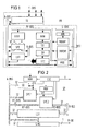
- FIG. 1 shows an example of the block diagram of a processor PR arranged on a chip, which contains a dual-port RAM memory SP in which operating data are stored.
- the dual-port RAM memory is connected to a first data bus (A-bus) and a second data bus (B-bus).
- A-bus first data bus
- B-bus second data bus
- the structure of such a processor is essentially known. It contains a micro program controller MST, which in turn has an address register ARG, a micro program RAM memory MRAM, a micro program ROM memory MROM and a sequencer MSQ.
- the microprogram control is constructed in the usual way and need not be explained further. It provides the individual microinstructions that are required to operate the processor.
- the processor also contains PR units by means of which the microinstructions are decoded.
- the microinstructions are first transferred to a microinstruction register MIR, from there they arrive in a decoder SD which generates the control signals from the microinstructions. These are temporarily stored in a decoder register DR and then forwarded in time to the individual units of the processor via a clock generator TDC.
- the traffic between the processor PR and the outside world is carried out via an interface unit IU, which is connected to an external bus E-bus.
- the memory SP is provided for receiving the operating data and has an address register RAR, a memory unit SPE and a logic unit LU1, in which a test evaluation circuit is also arranged.
- the E-bus consists of a data bus, an address bus and a control bus.
- the memory SP must also be checked during the self-test of the processor PR.
- self-test devices via which the self-test can be carried out are additionally arranged in the memory SP. These arrangements must be such that the operating data contained in the storage unit SPE are not destroyed during the self-test and it is additionally not necessary for the operating data contained in the storage units SPE to be read out from the processor PR during the self-test, e.g. to an external memory and have to be reloaded after the self-test. In particular, if the operating data are confidential data, it is safer if these operating data do not leave the processor, ie the chip, during the test.
- the dual-port memory unit SPE is implemented by two single-port RAMs SPE1 and SPE2, hereinafter referred to as memory modules.
- the first memory module SPE1 is connected to the A bus via a bidirectional bus (R1 bus), while the second memory module SPE2 is connected to the A bus via a unidirectional bus (R2 bus) and a unidirectional bus (R3 bus) connected to the B bus.
- the address inputs of the memory unit SPE are connected to the address register RAR, which is shown in FIG. 2 divided into two address registers.
- the test signals required for the test operation are generated with the aid of a switching element SG, which generates test signals from the addresses.
- the test responses of the storage unit SPE are evaluated in a logical unit LU1, which contains a signature register S-RG.
- a control device LSC is used to control the processes.
- identical data are stored in the memory modules SPE1 and SPE2. These can be, for example, intermediate results of the processor's work, keys or customer-specific parameters.
- the memory unit In test mode, the memory unit is separated into two memory modules, which are tested independently of one another.
- the SPE1 memory module can be tested first during the self-test.
- the address register RAR generates addresses which are fed to the address input of the memory module SPE1. These addresses can also be used to generate the test signals for the memory module SPE1. For this reason, the address signals are fed to the A bus via the switching element SG and from there to the data connection of the memory module SPE1.
- the test response signals then emitted by the memory module SPE1 are in turn transmitted to the logic unit LU1 via the A-bus and collected there in a signature register S-RG. After the testing of the memory module SPE1 has been completed, the signature is compared with a target signature and derived from it whether an error has occurred or not.
- the content of the memory module SPE2 is transferred to the memory module SPE1. These are the operating data contained in the SPE2 memory module. Now the SPE2 memory module can also be tested in accordance with the test of the SPE1 memory module. Address signals are in turn fed to the memory module SPE2 and test signals are generated from the address signals, which are fed via the A bus to the memory module at the data input. The test signals loaded in the memory module SPE2 are read out again and transmitted via the B-bus to the logic unit LU1 and collected there in the signature register S-RG. At the end of the test, the signature is compared with a target signature and the correctness is checked.
- the memory SP is designed so that the same test signals are written into the same memory locations of the memory modules SPE1 and SPE2; the target signature is therefore identical for both memory modules.
- the target signature can already be contained in the signature register S-RG, for example hard-wired. It is important that the respective content of a memory module to be tested is contained in the other memory module and is written back after the test. This ensures that the operating data are not lost during the self-test.
- W (A) means writing the memory location addressed with A with the value of the extended address A
- W (-A) means writing the memory location addressed with A with the inverted address A. Accordingly, R (A) is reading the memory location addressed with A. Memory location in the expectation that the extended address A is read out, or R (-A) read the memory location addressed with A with the expectation that the expected inverted address is read out.
- the algorithm is known from M. Marinescu, "Simple and Efficient Algorithms for Functional RAM Testung", IEEE Test Conference 1982, pp. 236-239.
- the address register RAR must be constructed as an up / down counter to execute this test algorithm.
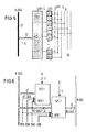
- FIG. 3 shows a possible exemplary embodiment.
- the address register is implemented with the aid of three up / down counters Z-A, Z-B, Z-C. It is of course also possible to use fewer counters.
- the counter Z-C can be used in the exemplary embodiment, the address signals of which are fed to the memory module SPE1 or the memory module SPE2 and from which the test signals are obtained. Accordingly, the outputs of the counters Z are connected to the corresponding memory units via multiplexer MUX2 in accordance with the operating mode selected with the aid of a selection signal SEL.
- the address register RAR is designed as a BILBO register so that it can perform different operating modes as a register, counter, signature register. It can work as a normal address register, to which the address signals are fed via the M-Bus, which are then stored in the counters Z and from there are fed unchanged to the memory unit.
- the counters Z do not work as counters, but as registers.
- the output of the counter is connected to the input via a logic unit LU2, that is to say a feedback is established.
- the feedback via the logical unit LU2 can be such that different counting sequences are generated.
- the feedback takes place via a multiplexer MUX1, which is controlled by selection signals BIL-S.
- the meter can be given four different operating modes via two selection signals, of which only two are of interest for testing the memory.
- the counting clocks for the counters are supplied as clock signals L1, L0. This is because each counting point consists of two latch stages LA1, LA2, which are clocked one after the other. Of course, it is also possible to implement each counting point as a flip-flop, so that only a single counting cycle would be required.
- a logic unit LU3 emits a signal RAR-U or RAR-D.
- RAR-U is given when the counter has counted down, RAR-D when it has counted up.
- the multiplexer MUX1 either receives the address signals from the M-Bus as X signals or the signals U or D fed back via the logic unit LU2.
- the latch stages LA1, LA2 are first reset with a reset signal RE-S.
- the signals X, U or D are then fed in via the multiplexer MUX1 and transferred to the latch stage LA1 with the aid of the clock signal L1.
- the transfer to LA2 takes place with the clock signal L0.
- the address signal A is taken from the latch stage LA1, while the signal Q to be fed back is taken from the latch stage LA2.
- RAR-U AND (Q4, NOR (Q3, Q2, Q1, Q0))
- RAR-D: AND (Q0, NOR (Q4, Q3, Q2, Q1,))
- the test signals T-S are also generated from the address signals A during the test. This takes place with the help of the switching element SG, which in the exemplary embodiment consists of e.g. five address signal bits 32 test signal bits by doubling.
- the address signals are fed to EXOR circuits EX1, which are additionally controlled by a control signal EX1-S.
- the test signals emitted by the EXOR circuits EX1 are then fed to the A bus via a driver stage TR1.
- the driver stage TR1 is controlled by a control signal TR1-S.
- the address signals can be fed to the A bus either unaffected or inverted as test signals.
- the detailed design of the storage unit SPE can be seen in FIG. 6.
- the memory modules SPE1 and SPE2 are implemented as single-port RAMs, of which SPE1 are connected to the A-bus, SPE2 to the A-bus and the B-bus.
- Address signals A which are generated by the address register RAR, are fed to the address inputs.
- a signal BSN is provided, by means of which the memory modules SPE1 and SPE2 are activated.
- Control signals TMA and TMB are used for the separate selection of the memory modules, the control signal TMA being fed only to the memory module SPE1 and the control signal TMB being fed only to the memory module SPE2.
- NOR linking By NOR linking (NOR 1) the signals BSN and TMA or BSN and TMB the separate selection of the memory modules is then ensured.
- the signal WN indicates whether the memory modules are written to or read from.
- the width of the addresses is 5 bits, while the width of the data is 32 bits.
- the logic unit LU1 which is the subject of FIG. 7, contains a latch stage LA31 or LA32 for the temporary storage of data from the A-bus or B-bus, a driver TR2 and the test signal evaluation circuit, consisting of a signature register S-RG, which also contains a comparator VGL. Via the driver TR2 it is possible to route data back to the A bus, for this purpose it is controlled by a control signal LUDR-S.
- the latch stages LA31, LA32 receive an enable signal LUEN-S.
- the logic unit LU1 is controlled by a control signal LUOP-S and switches through either the output of the latch stage LA31 or LA32 to the output in test mode.
- the data output by the memory module SPE 2 via the B bus can be transferred to the A bus and loaded from there into the memory module SPE1.
- the test response signals coming from the B bus or A bus can be fed to the test signal evaluation circuit.
- the signature register S-RG is composed of an EXOR element EX2 and two latch stages LA4 and LA5. A flip-flop can also take the place of the latch stages LA4 and LA5. Latch stages LA4 and LA5 are reset with the aid of a reset signal RE-S and clocked with the aid of clock signals LUSIG1 and LUSIG0. A feedback from the output to the input is provided to form the signature.
- the comparison circuit VGL consists of a NOR gate in which the target signature is hard-wired.
- the signature register S-RG has 32 levels corresponding to the 32 bits of the storage locations in the Storage units.
- the structure can be seen in FIG. 8.
- the outputs Q or Q are fed to the comparison circuit VGL, which compares these outputs with the target signature. In the case of equality, the comparison circuit then outputs the signal R-GO. It is also possible to read out the signature via the SIG output.
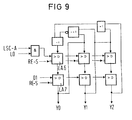
- the memory test algorithm is controlled by the control circuit LSC.
- An embodiment of the control circuit is shown in FIG. 9. It consists of latch stages LA6, LA7, which are interconnected in accordance with FIG.
- the latch stages LA are supplied with reset signals RE-S in order to bring them into an initial position.
- the signals L0 and D1 are used as counting clocks.
- the LSC-A signal is obtained by ORing the RAR-U and RAR-D signals. That is, the state of the control circuit LSC depends on the count of the up and down counter, which generates the addresses in test mode. In the exemplary embodiment, this is the counter Z-C.
- the control circuit is supplied with a self-test command that switches on the LSC.
- the mode of operation of the control circuit can be recognized and it can be determined when its output signals YO, Y1 and Y2 occur.
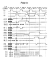
- the timing diagram of FIGS. 10 to 13 and the implementation of FIG. 9 it is readily possible to derive the point in time at which the control signals for the individual units of the memory occur.
- control circuit LSC is brought into a waiting state, this is done with the help of the reset signals RE-S.
- the control circuit becomes active when the signal LSC-A appears.
- the signals Y0, Y1, Y2 necessary for the test are generated with the subsequent signals L0 and D1.
- control circuit LSC then changes to state 1. From this point in time, the control circuit LSC takes over control over BSN and WN, over BIL-S, TRl-S as well as LUSIG0 and LUSIG1.
- the switching element SG is activated and the test signals derived from the addresses are written into the memory units.
- the signature register S-RAG remains inactive.
- the status of the address register RAR can also be seen in FIG. 10.
- phase 1 data, i.e. test signals, are written under all addresses of the memory units. As soon as all addresses have been counted, the address register issues the signal RAR-U and LSC thus goes into phase 2.
- phase 2 data are read out from the memory unit SPE and subsequently inverted address signals are written in as a test signal. From this point in time, the signature register S-RG also becomes active since test response signals are now present in the read phases. From phase 4, the up / down counter Z is switched over to down counting (FIG. 12).
- phase 4 only two addresses are read because the RAR-D signal follows immediately by changing the direction of travel. This phase is therefore only used for synchronization.
- the data can also be written to the A-bus inverted because the memory units are inactive during the write phases.
- the signature register remains active. In phase 5, however, the data must be created inverted ( Figure 12).
- control circuit LSC When the control circuit LSC is in state 7, the counter ZC sends the end signal RAR-D. The control circuit goes back to state 0 and the test process is finished. The change in the state of the control circuit LSC takes place after starting with a self-test command via the end criteria RAR-U and RAR-D, which are derived from the counter.
- the signals Y output by the control circuit LSC are e.g. also supplied to the decoder SD via the M-Bus, which converts them into control signals, which are then supplied to the individual units of the memory SP in the correct time by the time decoder TDC.
- the conversion into control signals is micro-programmed and can be carried out easily if the flow diagrams in FIGS. 10 to 13 are known.
- the self-test of the memory SP has been described in connection with the processor PR.
- the memory SP can of course also work together with other units. This makes sense in all applications in which dual-port RAM is subjected to a self-test and the operating data must be retained.
Landscapes
- Tests Of Electronic Circuits (AREA)
- For Increasing The Reliability Of Semiconductor Memories (AREA)
- Techniques For Improving Reliability Of Storages (AREA)
Applications Claiming Priority (2)
| Application Number | Priority Date | Filing Date | Title |
|---|---|---|---|
| DE4008345 | 1990-03-15 | ||
| DE4008345 | 1990-03-15 |
Publications (2)
| Publication Number | Publication Date |
|---|---|
| EP0446449A2 true EP0446449A2 (fr) | 1991-09-18 |
| EP0446449A3 EP0446449A3 (en) | 1992-07-01 |
Family
ID=6402307
Family Applications (1)
| Application Number | Title | Priority Date | Filing Date |
|---|---|---|---|
| EP19900124153 Withdrawn EP0446449A3 (en) | 1990-03-15 | 1990-12-13 | Dual-port memory suited for self-test and method for testing the same |
Country Status (1)
| Country | Link |
|---|---|
| EP (1) | EP0446449A3 (fr) |
Cited By (3)
| Publication number | Priority date | Publication date | Assignee | Title |
|---|---|---|---|---|
| EP0655744A1 (fr) * | 1993-11-01 | 1995-05-31 | Nec Corporation | Dispositif de mémoire multibit à semi-conducteurs |
| CN112305411A (zh) * | 2020-11-23 | 2021-02-02 | 珠海市一微半导体有限公司 | 一种i2s接口的功能测试电路及测试方法 |
| CN113325386A (zh) * | 2021-04-16 | 2021-08-31 | 上海宏景智驾信息科技有限公司 | Spad激光雷达双随机内存实时统计tdc的方法 |
Family Cites Families (2)
| Publication number | Priority date | Publication date | Assignee | Title |
|---|---|---|---|---|
| US3544777A (en) * | 1967-11-06 | 1970-12-01 | Trw Inc | Two memory self-correcting system |
| US4903266A (en) * | 1988-04-29 | 1990-02-20 | International Business Machines Corporation | Memory self-test |
-
1990
- 1990-12-13 EP EP19900124153 patent/EP0446449A3/de not_active Withdrawn
Cited By (4)
| Publication number | Priority date | Publication date | Assignee | Title |
|---|---|---|---|---|
| EP0655744A1 (fr) * | 1993-11-01 | 1995-05-31 | Nec Corporation | Dispositif de mémoire multibit à semi-conducteurs |
| US5535163A (en) * | 1993-11-01 | 1996-07-09 | Nec Corporation | Semiconductor memory device for inputting and outputting data in a unit of bits |
| CN112305411A (zh) * | 2020-11-23 | 2021-02-02 | 珠海市一微半导体有限公司 | 一种i2s接口的功能测试电路及测试方法 |
| CN113325386A (zh) * | 2021-04-16 | 2021-08-31 | 上海宏景智驾信息科技有限公司 | Spad激光雷达双随机内存实时统计tdc的方法 |
Also Published As
| Publication number | Publication date |
|---|---|
| EP0446449A3 (en) | 1992-07-01 |
Similar Documents
| Publication | Publication Date | Title |
|---|---|---|
| DE3490015C2 (fr) | ||
| DE2311034C2 (de) | Verfahren zum Prüfen eines integrierte logische Verknüpfungs- und Speicherglieder enthaltenden Halbleiterchips | |
| DE2747384C2 (de) | Datenverarbeitungseinheit mit Einrichtung zur Prüfung des Verarbeitungsabschnitts | |
| DE69329720T2 (de) | Transparentes testen von integrierten schaltkreisen | |
| DE3606650A1 (de) | Hardware logik-simulator | |
| DE2457553A1 (de) | Asynchroner taktgeber | |
| DE2719531B2 (de) | Digitale Logikschaltung zur Synchronisierung der Datenübertragung zwischen asynchrongesteuerten Datensystemen | |
| DE2717311A1 (de) | Datenprozessor | |
| DE3146721C2 (fr) | ||
| DE69131147T2 (de) | Verfahren zur Simulation des Zustands eines Schieberegisters mit linearer Rückkopplung | |
| DE3722907A1 (de) | Maximallaengen-schieberegister-folgegenerator | |
| DE19934500C2 (de) | Synchroner integrierter Speicher | |
| EP0446449A2 (fr) | Mémoire à double accès apte à l'auto-test et procédé de test de ladite mémoire | |
| DE3422287C2 (fr) | ||
| DE69126249T2 (de) | Verarbeitungsvorrichtung und Verfahren zur Programmierung einer solchen Vorrichtung | |
| DE10121165A1 (de) | Verfahren und Vorrichtung zum Initialisieren einer asynchronen Latch-Kette | |
| DE19948904C1 (de) | Schaltungszelle mit eingebauter Selbsttestfunktion und Verfahren zum Testen hierfür | |
| DE102004010562B4 (de) | Schnittstellenvorrichtung und Verfahren zur Synchronisation von Daten | |
| DE19513587B4 (de) | Speicherbauelement und Verfahren zum Programmieren eines Steuerbetriebsmerkmals eines Speicherbauelements | |
| WO1988009554A1 (fr) | Procede et agencement de controle automatique de memoires vives organisees par mots | |
| DE19948598B4 (de) | Mikrocomputer mit Abtastfunktion eines Wiederholungs-Anforderungssignals in Synchronisation mit einem Abtastsignal | |
| DE102009041815B4 (de) | Verfahren zur Erzeugung einer Schaltung aus einer Darstellung von Eigenschaften in einem Eigenschaftsgraphen | |
| DE10052210A1 (de) | Integrierte Schaltung mit einer synchronen und asynchronen Schaltung sowie Verfahren zum Betrieb einer solchen integrierten Schaltung | |
| WO1993003434A1 (fr) | Procede de verification de circuits integres avec au moins un circuit logique et circuit integre testable | |
| DE68923843T2 (de) | Synchroner logischer schaltkreis mit übertragungssignalsteuerung. |
Legal Events
| Date | Code | Title | Description |
|---|---|---|---|
| PUAI | Public reference made under article 153(3) epc to a published international application that has entered the european phase |
Free format text: ORIGINAL CODE: 0009012 |
|
| 17P | Request for examination filed |
Effective date: 19901213 |
|
| AK | Designated contracting states |
Kind code of ref document: A2 Designated state(s): DE FR GB NL |
|
| PUAL | Search report despatched |
Free format text: ORIGINAL CODE: 0009013 |
|
| AK | Designated contracting states |
Kind code of ref document: A3 Designated state(s): DE FR GB NL |
|
| STAA | Information on the status of an ep patent application or granted ep patent |
Free format text: STATUS: THE APPLICATION HAS BEEN WITHDRAWN |
|
| 17Q | First examination report despatched |
Effective date: 19941004 |
|
| 18W | Application withdrawn |
Withdrawal date: 19941013 |