EP0444720B1 - Sensormatrix - Google Patents
Sensormatrix Download PDFInfo
- Publication number
- EP0444720B1 EP0444720B1 EP91200110A EP91200110A EP0444720B1 EP 0444720 B1 EP0444720 B1 EP 0444720B1 EP 91200110 A EP91200110 A EP 91200110A EP 91200110 A EP91200110 A EP 91200110A EP 0444720 B1 EP0444720 B1 EP 0444720B1
- Authority
- EP
- European Patent Office
- Prior art keywords
- sensors
- electrode
- matrix
- electrodes
- semiconductor layer
- Prior art date
- Legal status (The legal status is an assumption and is not a legal conclusion. Google has not performed a legal analysis and makes no representation as to the accuracy of the status listed.)
- Expired - Lifetime
Links
- 239000011159 matrix material Substances 0.000 claims description 37
- 239000004065 semiconductor Substances 0.000 claims description 27
- 230000035945 sensitivity Effects 0.000 claims description 4
- 239000010409 thin film Substances 0.000 claims description 4
- BUGBHKTXTAQXES-UHFFFAOYSA-N Selenium Chemical compound [Se] BUGBHKTXTAQXES-UHFFFAOYSA-N 0.000 claims description 2
- 239000000463 material Substances 0.000 claims description 2
- 229910052711 selenium Inorganic materials 0.000 claims description 2
- 239000011669 selenium Substances 0.000 claims description 2
- 230000005669 field effect Effects 0.000 description 10
- 238000005516 engineering process Methods 0.000 description 3
- 238000004519 manufacturing process Methods 0.000 description 3
- 230000005855 radiation Effects 0.000 description 3
- 241001136792 Alle Species 0.000 description 2
- 238000010586 diagram Methods 0.000 description 2
- OAICVXFJPJFONN-UHFFFAOYSA-N Phosphorus Chemical compound [P] OAICVXFJPJFONN-UHFFFAOYSA-N 0.000 description 1
- 238000005352 clarification Methods 0.000 description 1
- 230000000694 effects Effects 0.000 description 1
- 230000012447 hatching Effects 0.000 description 1
- 230000002787 reinforcement Effects 0.000 description 1
- 230000001960 triggered effect Effects 0.000 description 1
- 239000002699 waste material Substances 0.000 description 1
Images
Classifications
-
- H—ELECTRICITY
- H10—SEMICONDUCTOR DEVICES; ELECTRIC SOLID-STATE DEVICES NOT OTHERWISE PROVIDED FOR
- H10F—INORGANIC SEMICONDUCTOR DEVICES SENSITIVE TO INFRARED RADIATION, LIGHT, ELECTROMAGNETIC RADIATION OF SHORTER WAVELENGTH OR CORPUSCULAR RADIATION
- H10F77/00—Constructional details of devices covered by this subclass
- H10F77/20—Electrodes
- H10F77/206—Electrodes for devices having potential barriers
-
- H—ELECTRICITY
- H10—SEMICONDUCTOR DEVICES; ELECTRIC SOLID-STATE DEVICES NOT OTHERWISE PROVIDED FOR
- H10F—INORGANIC SEMICONDUCTOR DEVICES SENSITIVE TO INFRARED RADIATION, LIGHT, ELECTROMAGNETIC RADIATION OF SHORTER WAVELENGTH OR CORPUSCULAR RADIATION
- H10F39/00—Integrated devices, or assemblies of multiple devices, comprising at least one element covered by group H10F30/00, e.g. radiation detectors comprising photodiode arrays
- H10F39/10—Integrated devices
- H10F39/12—Image sensors
- H10F39/18—Complementary metal-oxide-semiconductor [CMOS] image sensors; Photodiode array image sensors
Definitions
- the invention relates to a sensor matrix according to the preamble of claim 1.
- a sensor matrix is known in which the first electrodes the sensors in one direction, for example in the row direction, and the second electrodes in one direction 90 ° to the first direction, for example in the column direction, are connected. Are between the two electrodes several, stacked semiconductor layers are provided.
- the X-ray sensitivity of this sensor matrix is achieved in that on the outer electrode a luminescent layer is provided, which on impact emitted by X-rays, which in turn generates the desired reaction in the semiconductor layers.
- X-ray radiation is here indirectly by means of a Luminous layer measured.
- Each sensor element therefore has a first electrode, which of the first electrodes of all other sensor elements is mechanically and electrically separated and which is only effective for one sensor element.
- sensors in the matrix are for each sensor corresponding individual electrodes are arranged next to one another provided as the first electrodes.
- These first Electrodes of the sensors are by means of a semiconductor layer covered, which consistently for all sensors is formed, which is not interrupted or otherwise is divided.
- the second electrodes of the sensors are again formed by a continuous layer, which effective at least for groups of sensors is. For example, for a group of ten sensors one common second electrode may be provided. This The electrode is then in one piece for the ten sensors. in the In extreme cases, this second electrode can be used for all sensors the matrix together as a single electrode be.
- the arrangement gives the advantage of being strong simplified manufacturing.
- the semiconductor layer and the second electrodes are each as one layer executed, which need not be structured.
- For the individual sensors are only their first electrodes, as well as one that may be specified for each sensor Switching element, to be provided individually for each sensor.
- the second electrode formed as a continuous layer the semiconductor layer in the region of the first electrodes covers all sensors of the matrix and for all Sensors of the matrix as a common second electrode is effective.
- the Sensors that are formed together for all sensors Semiconductor layer is so thick that it itself sufficiently absorbed x-rays, and that none additional phosphor layer is provided.
- the desired X-ray sensitivity of the semiconductor layer can, as in a further embodiment the invention is provided, advantageously by means of a suitably doped selenium are generated that in a thickness of about 0.5 mm is to be provided.
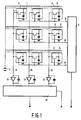
- a basic circuit diagram of a Sensor matrix for all sensor elements of the matrix a common semiconductor layer and also one common second electrode are provided Sensors 1, which are in rows and columns in the matrix are arranged.
- the individual sensors 1 of the matrix are constructed in an identical manner.
- Each sensor 1 has one first electrode 2, which only in the area of respective sensor 1 is provided, and which of the first electrodes 2 of the adjacent sensors 1 mechanically and is electrically isolated.
- Each of the first electrodes 2 is in the respective sensor 1 with a first electrode a storage capacity 3 connected, the other Electrode is grounded.
- the connection between the first electrode 2 and the storage capacity 3 is with a source connection of a field effect transistor 4 connected.
- a sensor matrix for example, 2000 x 2000 such sensors may be provided.
- Fig. 1 takes into account only three for clarification Sensors per row and column.
- All sensors in the matrix are, as in FIG. 1 is indicated schematically, by means of a Semiconductor layer 5 covered, at least all first electrodes 2 of all sensor elements 1 of the matrix covers.
- the semiconductor layer 5 in turn is by means of an electrically conductive layer 6, which serves as a second electrode for all sensors 1 Matrix is effective as such.
- the second electrode 6 is connected to a DC voltage source 7, the other Pole is grounded.
- the sensor matrix shown schematically in FIG. 1 is in Thin-film technology manufactured. This doesn't just apply to the two electrodes as well as the semiconductor layer, but also for storage capacities 3 and Field effect transistors 4.
- the second common for all sensors in the matrix Electrode 6 is by means of the DC voltage source 7 biased. Strikes the semiconductor layer 5 light or X-rays, this is from the Semiconductor layer absorbs and changes their Conductivity. It finds a charge shift instead, which leads to the storage capacities 3 the sensors 1 are electrically charged.
- the high of Charging each individual sensor depends on how much Radiation onto the semiconductor layer 5 in the area between the first electrode 2 of this sensor and the Counter electrode 6 in a certain time period has hit.
- the charges stored in the storage capacities 3 can be read out to determine the incident radiation become.
- Switching line 8 is provided, which with the gate connections the field effect transistors of the sensors of their Line are connected and which by means of a control circuit 9 can be controlled.
- the control circuit 9 can for example the switching line 8 of the first line activate so that all field effect transistors 4 of the Sensors of this line are switched on.
- the field effect transistors of the sensors in their column connected readout line 10 read out. So it takes place a readout instead, which is for all sensors in this line done simultaneously.
- After reinforcement of the read out Signals in amplifiers 11 get these amplified Form in a multiplex circuit 12, which from the parallel incoming data from the sensor columns serial output signal forms.
- Fig. 1 are for the clearest possible representation of the electrical switching principle both the semiconductor layer 5, as well as the common second electrode 6 shown in several parts. In fact, however, both are each made in one piece and cover all first electrodes 2 of all sensors 1 of the matrix.
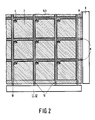
- FIG. 2 This state of affairs is shown in the illustration according to FIG. 2 to recognize even more clearly the supervision of a Shows part of a matrix according to the invention.
- the matrix is in view of the common second counter electrode 6 shown.
- Both the counter electrode 6 and the common semiconductor layer 5 cover all the first Electrodes 2 of the sensors of the matrix, of which in the 2 only nine are shown as examples.
- To the underlying elements of the sensors represent 2 are the second in the illustration according to FIG Electrode 6 and the semiconductor layer 5 only in hatching and presented almost transparent.
- the first Electrodes 2 of the sensors are therefore shown 2 directly with the source connections of the Field effect transistors 4 connected.
- the gate connections the field effect transistors 4 are each with a Switching line 8 connected while the drain connections the field effect transistors each with a readout line 10 are connected.
- the arrangement according to FIG. 2 is produced using thin film technology. This applies to all elements of the sensors, So also for the field effect transistors 4 and for the for each sensor individually provided first Electrodes 2. Also manufactured using thin-film technology are both the first electrodes of the sensors covering semiconductor layer as well as that on this provided electrically conductive layer 6, which for all sensors of the matrix as a common second electrode serves.
- a common continuous Layer should only be provided for a group of sensors. So can for example for a group of 100 x 100 sensors a common counter electrode 6 may be provided. The same applies to other groups of sensors, which in turn is a common one intended for it have second electrode 6. Such a group of Sensors can also be one of all sensors, for example Column or row are formed.
Landscapes
- Solid State Image Pick-Up Elements (AREA)
- Measurement Of Radiation (AREA)
Description
Claims (4)
- Sensormatrix mit in Dünnschichttechnik erzeugten, in Zeilen und Spalten angeordneten, licht- und/oder röntgenstrahlenempfindlichen Sensoren (1), welche zwei Elektroden (2,6) und eine zwischen diesen angeordnete Halbleiterschicht (5) aufweisen,
dadurch gekennzeichnet, daßjeder Sensor (1) jeweils eine Einzelelektrode als erste Elektrode (2) sowie ein Schaltelement (4) umfaßt,die ersten Elektroden (2) der Sensoren einer Spalte bzw. Zeile über die Schaltelemente (4) mit einer gemeinsamen Ausleseleitung (10) verbunden sind,die Schaltelemente einer Zeile bzw. Spalte an eine gemeinsame Schaltleitung (8) zum Schalten der Schaltelemente (4) angeschlossen sind,die Halbleiterschicht (5) durchgehend für alle Sensoren (1) als gemeinsame Schicht gebildet ist und alle ersten Elektroden (2) abdeckt unddie zweite Elektrode (6) wenigstens für Gruppen der Sensoren (1) als eine durchgehende Schicht (6) gebildet ist, die jeweils die Halbleiterschicht (5) im Bereich aller ersten Elektroden (2) der Sensoren ihrer Gruppe abdeckt und für alle Sensoren ihrer Gruppe als zweite Elektrode wirksam ist. - Sensormatrix nach Anspruch 1,
dadurch gekennzeichnet, daß die zweite, als durchgehende Schicht gebildete Elektrode die Halbleiterschicht (5) im Bereich der ersten Elektroden (2) aller Sensoren (1) der Matrix abdeckt und für alle Sensoren (1) der Matrix als gemeinsame zweite Elektrode (6) wirksam ist. - Sensormatrix nach Anspruch 1 oder 2,
dadurch gekennzeichnet, daß für Röntgenstrahl-Empfindlichkeit der Sensoren die gemeinsam für alle Sensoren (1) gebildete Halbleiterschicht so dick ausgeführt ist, daß sie selbst ausreichend Röntgenstrahlen absorbiert, und daß keine zusätzliche Leuchtstoffschicht vorgesehen ist. - Sensormatrix nach Anspruch 3,
dadurch gekennzeichnet, daß als Halbleitermaterial (5) geeignet dotiertes Selen vorgesehen ist und daß die Halbleiterschicht eine Dicke von etwa 0,5 mm aufweist.
Applications Claiming Priority (2)
| Application Number | Priority Date | Filing Date | Title |
|---|---|---|---|
| DE4002429A DE4002429A1 (de) | 1990-01-27 | 1990-01-27 | Sensormatrix |
| DE4002429 | 1990-01-27 |
Publications (2)
| Publication Number | Publication Date |
|---|---|
| EP0444720A1 EP0444720A1 (de) | 1991-09-04 |
| EP0444720B1 true EP0444720B1 (de) | 1999-04-14 |
Family
ID=6398922
Family Applications (1)
| Application Number | Title | Priority Date | Filing Date |
|---|---|---|---|
| EP91200110A Expired - Lifetime EP0444720B1 (de) | 1990-01-27 | 1991-01-21 | Sensormatrix |
Country Status (4)
| Country | Link |
|---|---|
| US (1) | US5132541A (de) |
| EP (1) | EP0444720B1 (de) |
| JP (1) | JP3313375B2 (de) |
| DE (2) | DE4002429A1 (de) |
Families Citing this family (39)
| Publication number | Priority date | Publication date | Assignee | Title |
|---|---|---|---|---|
| US5260592A (en) * | 1991-02-19 | 1993-11-09 | Synaptics, Incorporated | Integrating photosensor and imaging system having wide dynamic range with varactors |
| US5324958A (en) * | 1991-02-19 | 1994-06-28 | Synaptics, Incorporated | Integrating imaging systgem having wide dynamic range with sample/hold circuits |
| FR2679687B1 (fr) * | 1991-07-26 | 1997-03-14 | Commissariat Energie Atomique | Dispositif ou prise opu d'affichage d'images en grande dimension. |
| US5254480A (en) * | 1992-02-20 | 1993-10-19 | Minnesota Mining And Manufacturing Company | Process for producing a large area solid state radiation detector |
| DE4227096A1 (de) * | 1992-08-17 | 1994-02-24 | Philips Patentverwaltung | Röntgenbilddetektor |
| US5596200A (en) * | 1992-10-14 | 1997-01-21 | Primex | Low dose mammography system |
| AU6574694A (en) * | 1993-04-28 | 1994-11-21 | University Of Surrey | Radiation detectors |
| JP3431995B2 (ja) * | 1993-06-03 | 2003-07-28 | キヤノン株式会社 | 撮像装置 |
| GB9414639D0 (en) * | 1994-07-20 | 1994-09-07 | Philips Electronics Uk Ltd | An image detector |
| WO1997042661A1 (en) | 1996-05-08 | 1997-11-13 | 1294339 Ontario Inc. | High resolution flat panel for radiation imaging |
| US5744807A (en) * | 1996-06-20 | 1998-04-28 | Xerox Corporation | Sensor array data line readout with reduced crosstalk |
| JP2000509627A (ja) | 1997-02-14 | 2000-08-02 | コーニンクレッカ フィリップス エレクトロニクス エヌ ヴィ | 従来のラジオグラフィ用の手段を有するx線スキャナー |
| WO1998048599A2 (en) * | 1997-04-24 | 1998-10-29 | Koninklijke Philips Electronics N.V. | Exposure control on the basis of a relevant part of an x-ray image |
| GB9710301D0 (en) * | 1997-05-21 | 1997-07-16 | Philips Electronics Nv | Image sensor and its manufacture |
| US6486470B2 (en) | 1998-11-02 | 2002-11-26 | 1294339 Ontario, Inc. | Compensation circuit for use in a high resolution amplified flat panel for radiation imaging |
| JP3683463B2 (ja) | 1999-03-11 | 2005-08-17 | シャープ株式会社 | アクティブマトリクス基板、その製造方法、及び、該基板を用いたイメージセンサ |
| JP3916823B2 (ja) | 1999-04-07 | 2007-05-23 | シャープ株式会社 | アクティブマトリクス基板およびその製造方法、並びにフラットパネル型イメージセンサ |
| DE19926582A1 (de) * | 1999-06-11 | 2000-12-14 | Philips Corp Intellectual Pty | Sensor |
| US20020121605A1 (en) * | 1999-06-17 | 2002-09-05 | Lutz Fink | Semiconductor sensor and method for its wiring |
| DE19927694C1 (de) | 1999-06-17 | 2000-11-02 | Lutz Fink | Halbleitersensor mit einer Pixelstruktur |
| JP2001095790A (ja) * | 1999-09-30 | 2001-04-10 | Shimadzu Corp | X線透視撮影装置 |
| JP3581073B2 (ja) | 2000-03-07 | 2004-10-27 | シャープ株式会社 | イメージセンサおよびその製造方法 |
| JP2002162474A (ja) | 2000-11-27 | 2002-06-07 | Sharp Corp | 電磁波検出器およびその製造方法 |
| US6774448B1 (en) * | 2000-11-30 | 2004-08-10 | Optical Communication Products, Inc. | High speed detectors having integrated electrical components |
| DE10142531A1 (de) | 2001-08-30 | 2003-03-20 | Philips Corp Intellectual Pty | Sensoranordnung aus licht- und/oder röntgenstrahlungsempfindlichen Sensoren |
| CA2363663C (en) * | 2001-11-22 | 2004-10-19 | Ftni Inc. | Direct conversion flat panel x-ray detector with automatic cancellation of ghost images |
| US7763208B2 (en) * | 2003-11-12 | 2010-07-27 | E.I. Du Pont De Nemours And Company | System and method for sensing and analyzing gases |
| US8236246B2 (en) * | 2004-10-07 | 2012-08-07 | E I Du Pont De Nemours And Company | Gas sensitive apparatus |
| WO2006085230A1 (en) * | 2005-02-08 | 2006-08-17 | Koninklijke Philips Electronics N.V. | Lead oxide based photosensitive device and its manufacturing method |
| US7122803B2 (en) * | 2005-02-16 | 2006-10-17 | Hologic, Inc. | Amorphous selenium flat panel x-ray imager for tomosynthesis and static imaging |
| US7233005B2 (en) * | 2005-02-16 | 2007-06-19 | Hologic, Inc. | Amorphous selenium flat panel x-ray imager for tomosynthesis and static imaging |
| US7304308B2 (en) * | 2005-02-16 | 2007-12-04 | Hologic, Inc. | Amorphous selenium flat panel x-ray imager for tomosynthesis and static imaging |
| US7759628B2 (en) | 2007-06-22 | 2010-07-20 | Seiko Epson Corporation | Detection device and electronic apparatus having plural scanning lines, detection lines, power supply lines and plural unit circuits arranged on a substrate |
| KR101218089B1 (ko) * | 2007-12-07 | 2013-01-18 | 엘지디스플레이 주식회사 | 디지털 엑스레이 디텍터 및 그 제조방법 |
| TWI464788B (zh) * | 2011-12-22 | 2014-12-11 | Ind Tech Res Inst | 感測元件陣列及其製作方法 |
| WO2017046390A1 (en) | 2015-09-17 | 2017-03-23 | Koninklijke Philips N.V. | Method for producing a radiation detector and radiation detector |
| EP3863059B1 (de) * | 2020-02-04 | 2024-07-31 | Siemens Healthineers AG | Perowskit-basierte detektoren mit erhöhter adhäsion |
| EP3863054A1 (de) | 2020-02-04 | 2021-08-11 | Siemens Healthcare GmbH | Multiple spektrale detektoren mittels strukturierter perowskite |
| KR102567702B1 (ko) * | 2021-06-30 | 2023-08-18 | 한국원자력연구원 | 방사선 검출소자 및 이의 제조방법 |
Citations (3)
| Publication number | Priority date | Publication date | Assignee | Title |
|---|---|---|---|---|
| WO1988000759A1 (en) * | 1986-07-24 | 1988-01-28 | Eastman Kodak Company | Electronic shutter for image sensor using photodiodes |
| US4862237A (en) * | 1983-01-10 | 1989-08-29 | Seiko Epson Corporation | Solid state image sensor |
| EP0558117A2 (de) * | 1992-02-24 | 1993-09-01 | Philips Patentverwaltung GmbH | Verfahren zum Erzeugen von Röntgenaufnahmen und Röntgengerät zur Durchführung des Verfahrens |
Family Cites Families (18)
| Publication number | Priority date | Publication date | Assignee | Title |
|---|---|---|---|---|
| US4032947A (en) * | 1971-10-20 | 1977-06-28 | Siemens Aktiengesellschaft | Controllable charge-coupled semiconductor device |
| JPS5226974B2 (de) * | 1973-02-14 | 1977-07-18 | ||
| GB1532859A (en) * | 1976-03-30 | 1978-11-22 | Mullard Ltd | Charge coupled circuit arrangements and devices |
| JPS58105672A (ja) * | 1981-12-17 | 1983-06-23 | Fuji Photo Film Co Ltd | 半導体撮像装置 |
| JPS58117478A (ja) * | 1982-01-05 | 1983-07-13 | Fuji Xerox Co Ltd | 放射線ctスキャナ装置用放射線センサアレイ |
| JPS60123059A (ja) * | 1983-12-08 | 1985-07-01 | Toshiba Corp | 密着型カラ−イメ−ジセンサ |
| EP0161324B1 (de) * | 1984-05-14 | 1987-11-25 | Matsushita Electric Industrial Co., Ltd. | Verfahren und Einrichtung mit Strahenquantenzählung |
| FR2564674B1 (fr) * | 1984-05-18 | 1986-09-19 | Thomson Csf | Barrette multilineaire a transfert de charge et procede d'analyse |
| US4794443A (en) * | 1984-05-28 | 1988-12-27 | Canon Kabushiki Kaisha | Semiconductor device and process for producing same |
| JPS6152061A (ja) * | 1984-08-22 | 1986-03-14 | Toshiba Corp | 密着型カラ−イメ−ジセンサ |
| US4835587A (en) * | 1984-09-19 | 1989-05-30 | Fuji Electric Co., Ltd. | Semiconductor device for detecting radiation |
| US4956687A (en) * | 1986-06-26 | 1990-09-11 | Santa Barbara Research Center | Backside contact blocked impurity band detector |
| US4831257A (en) * | 1986-09-26 | 1989-05-16 | Honeywell Inc. | Gate coupled input circuit |
| JPS63172462A (ja) * | 1987-01-12 | 1988-07-16 | Fujitsu Ltd | イメ−ジセンサの製造方法 |
| DE3885653T2 (de) * | 1987-05-26 | 1994-06-01 | Matsushita Electric Ind Co Ltd | Strahlungsdetektor. |
| FR2628562A1 (fr) * | 1988-03-11 | 1989-09-15 | Thomson Csf | Dispositif d'imagerie a structure matricielle |
| GB8812955D0 (en) * | 1988-06-01 | 1988-10-05 | Emi Plc Thorn | Thermal imaging |
| US5017989A (en) * | 1989-12-06 | 1991-05-21 | Xerox Corporation | Solid state radiation sensor array panel |
-
1990
- 1990-01-27 DE DE4002429A patent/DE4002429A1/de not_active Withdrawn
-
1991
- 1991-01-21 EP EP91200110A patent/EP0444720B1/de not_active Expired - Lifetime
- 1991-01-21 DE DE59109121T patent/DE59109121D1/de not_active Expired - Lifetime
- 1991-01-23 US US07/644,712 patent/US5132541A/en not_active Expired - Lifetime
- 1991-01-24 JP JP00704591A patent/JP3313375B2/ja not_active Expired - Lifetime
Patent Citations (3)
| Publication number | Priority date | Publication date | Assignee | Title |
|---|---|---|---|---|
| US4862237A (en) * | 1983-01-10 | 1989-08-29 | Seiko Epson Corporation | Solid state image sensor |
| WO1988000759A1 (en) * | 1986-07-24 | 1988-01-28 | Eastman Kodak Company | Electronic shutter for image sensor using photodiodes |
| EP0558117A2 (de) * | 1992-02-24 | 1993-09-01 | Philips Patentverwaltung GmbH | Verfahren zum Erzeugen von Röntgenaufnahmen und Röntgengerät zur Durchführung des Verfahrens |
Also Published As
| Publication number | Publication date |
|---|---|
| US5132541A (en) | 1992-07-21 |
| JPH04212458A (ja) | 1992-08-04 |
| EP0444720A1 (de) | 1991-09-04 |
| DE4002429A1 (de) | 1991-08-01 |
| DE59109121D1 (de) | 1999-05-20 |
| JP3313375B2 (ja) | 2002-08-12 |
Similar Documents
| Publication | Publication Date | Title |
|---|---|---|
| EP0444720A1 (de) | Sensormatrix | |
| EP0588397B1 (de) | Röntgenbilddetektor | |
| EP0440282B1 (de) | Sensormatrix | |
| DE69522013T2 (de) | Ausleseschaltung für eine bildmatrix mit aktiver matrix | |
| DE2755151C3 (de) | Flüssigkristall-Bildschirm mit Matrix-Ansteuerung | |
| DE69526457T2 (de) | Bilddetektor | |
| DE69216551T2 (de) | Analoge Schaltkreise mit geschalteter Kapazität | |
| DE69411914T2 (de) | Pixelanordnung, welche die bilderzeugenden pixelelemente integral mit den peripheren schaltkreiselementen hat | |
| DE3855168T2 (de) | Aktives Farb-Flüssigkristallanzeigeelement | |
| DE60033894T2 (de) | Strahlungsdetektor | |
| DE3425377C2 (de) | Pyroelektrischer Detektor | |
| DE3521917C2 (de) | Festkörper-Bildsensor | |
| DE3784991T2 (de) | Schaltkreis für ein photoempfindliches Pixel mit einem belichteten Blockierglied. | |
| EP0303819B1 (de) | Integrierte Schaltung zum Auslesen eines optoelektronischen Bildsensors | |
| EP0233464B1 (de) | Schaltung zum Auslesen eines optoelektronischen Bildsensors | |
| DE69634712T2 (de) | Schalttransistor für eine Festkörperbildaufnahmevorrichtung | |
| EP0027545B1 (de) | Monolithisch integrierte Schaltung zur zeilenweisen Bildabtastung und Verfahren zu deren Betrieb | |
| DE3910462C2 (de) | ||
| WO1995008190A1 (de) | Halbleiter(detektor)struktur | |
| DE69012382T2 (de) | Referenzzelle für das Lesen von EEPROM-Speicheranordnungen. | |
| DE2928253A1 (de) | Elektronisches adressiersystem zum lesen von mosaikmatrizen optoelektronischer elemente | |
| WO2000070864A1 (de) | Sensormatrix | |
| EP1059671B1 (de) | Röntgenstrahlbildsensor | |
| DE3688520T2 (de) | Festkoerperbildsensor mit amorpher, halbleitender, photoleitender zellenmatrix. | |
| DE19944731A1 (de) | Flächenhafter Bilddetektor für elektromagnetische Strahlen |
Legal Events
| Date | Code | Title | Description |
|---|---|---|---|
| PUAI | Public reference made under article 153(3) epc to a published international application that has entered the european phase |
Free format text: ORIGINAL CODE: 0009012 |
|
| AK | Designated contracting states |
Kind code of ref document: A1 Designated state(s): DE FR GB IT NL |
|
| 17P | Request for examination filed |
Effective date: 19920228 |
|
| 17Q | First examination report despatched |
Effective date: 19940505 |
|
| GRAG | Despatch of communication of intention to grant |
Free format text: ORIGINAL CODE: EPIDOS AGRA |
|
| RAP3 | Party data changed (applicant data changed or rights of an application transferred) |
Owner name: PHILIPS PATENTVERWALTUNG GMBH Owner name: KONINKLIJKE PHILIPS ELECTRONICS N.V. |
|
| GRAG | Despatch of communication of intention to grant |
Free format text: ORIGINAL CODE: EPIDOS AGRA |
|
| GRAG | Despatch of communication of intention to grant |
Free format text: ORIGINAL CODE: EPIDOS AGRA |
|
| GRAH | Despatch of communication of intention to grant a patent |
Free format text: ORIGINAL CODE: EPIDOS IGRA |
|
| GRAH | Despatch of communication of intention to grant a patent |
Free format text: ORIGINAL CODE: EPIDOS IGRA |
|
| GRAA | (expected) grant |
Free format text: ORIGINAL CODE: 0009210 |
|
| AK | Designated contracting states |
Kind code of ref document: B1 Designated state(s): DE FR GB IT NL |
|
| PG25 | Lapsed in a contracting state [announced via postgrant information from national office to epo] |
Ref country code: IT Free format text: LAPSE BECAUSE OF FAILURE TO SUBMIT A TRANSLATION OF THE DESCRIPTION OR TO PAY THE FEE WITHIN THE PRESCRIBED TIME-LIMIT;WARNING: LAPSES OF ITALIAN PATENTS WITH EFFECTIVE DATE BEFORE 2007 MAY HAVE OCCURRED AT ANY TIME BEFORE 2007. THE CORRECT EFFECTIVE DATE MAY BE DIFFERENT FROM THE ONE RECORDED. Effective date: 19990414 Ref country code: NL Free format text: LAPSE BECAUSE OF FAILURE TO SUBMIT A TRANSLATION OF THE DESCRIPTION OR TO PAY THE FEE WITHIN THE PRESCRIBED TIME-LIMIT Effective date: 19990414 |
|
| REF | Corresponds to: |
Ref document number: 59109121 Country of ref document: DE Date of ref document: 19990520 |
|
| GBT | Gb: translation of ep patent filed (gb section 77(6)(a)/1977) |
Effective date: 19990610 |
|
| ET | Fr: translation filed | ||
| NLV1 | Nl: lapsed or annulled due to failure to fulfill the requirements of art. 29p and 29m of the patents act | ||
| RAP4 | Party data changed (patent owner data changed or rights of a patent transferred) |
Owner name: KONINKLIJKE PHILIPS ELECTRONICS N.V. Owner name: PHILIPS CORPORATE INTELLECTUAL PROPERTY GMBH |
|
| PLBE | No opposition filed within time limit |
Free format text: ORIGINAL CODE: 0009261 |
|
| STAA | Information on the status of an ep patent application or granted ep patent |
Free format text: STATUS: NO OPPOSITION FILED WITHIN TIME LIMIT |
|
| 26N | No opposition filed | ||
| REG | Reference to a national code |
Ref country code: GB Ref legal event code: IF02 |
|
| PGFP | Annual fee paid to national office [announced via postgrant information from national office to epo] |
Ref country code: FR Payment date: 20100212 Year of fee payment: 20 |
|
| PGFP | Annual fee paid to national office [announced via postgrant information from national office to epo] |
Ref country code: GB Payment date: 20100129 Year of fee payment: 20 |
|
| PGFP | Annual fee paid to national office [announced via postgrant information from national office to epo] |
Ref country code: DE Payment date: 20100331 Year of fee payment: 20 |
|
| REG | Reference to a national code |
Ref country code: GB Ref legal event code: PE20 Expiry date: 20110120 |
|
| PG25 | Lapsed in a contracting state [announced via postgrant information from national office to epo] |
Ref country code: GB Free format text: LAPSE BECAUSE OF EXPIRATION OF PROTECTION Effective date: 20110120 |
|
| PG25 | Lapsed in a contracting state [announced via postgrant information from national office to epo] |
Ref country code: DE Free format text: LAPSE BECAUSE OF EXPIRATION OF PROTECTION Effective date: 20110121 |