EP0444531A2 - Process for multi-layer photoresist etching with minimal feature undercut and unchanging photoresist load during etch - Google Patents
Process for multi-layer photoresist etching with minimal feature undercut and unchanging photoresist load during etch Download PDFInfo
- Publication number
- EP0444531A2 EP0444531A2 EP91102541A EP91102541A EP0444531A2 EP 0444531 A2 EP0444531 A2 EP 0444531A2 EP 91102541 A EP91102541 A EP 91102541A EP 91102541 A EP91102541 A EP 91102541A EP 0444531 A2 EP0444531 A2 EP 0444531A2
- Authority
- EP
- European Patent Office
- Prior art keywords
- layer
- photoresist
- photoresist layer
- pattern
- etch
- Prior art date
- Legal status (The legal status is an assumption and is not a legal conclusion. Google has not performed a legal analysis and makes no representation as to the accuracy of the status listed.)
- Granted
Links
Images
Classifications
-
- H—ELECTRICITY
- H01—ELECTRIC ELEMENTS
- H01L—SEMICONDUCTOR DEVICES NOT COVERED BY CLASS H10
- H01L21/00—Processes or apparatus adapted for the manufacture or treatment of semiconductor or solid state devices or of parts thereof
- H01L21/02—Manufacture or treatment of semiconductor devices or of parts thereof
- H01L21/04—Manufacture or treatment of semiconductor devices or of parts thereof the devices having at least one potential-jump barrier or surface barrier, e.g. PN junction, depletion layer or carrier concentration layer
- H01L21/18—Manufacture or treatment of semiconductor devices or of parts thereof the devices having at least one potential-jump barrier or surface barrier, e.g. PN junction, depletion layer or carrier concentration layer the devices having semiconductor bodies comprising elements of Group IV of the Periodic System or AIIIBV compounds with or without impurities, e.g. doping materials
- H01L21/30—Treatment of semiconductor bodies using processes or apparatus not provided for in groups H01L21/20 - H01L21/26
- H01L21/302—Treatment of semiconductor bodies using processes or apparatus not provided for in groups H01L21/20 - H01L21/26 to change their surface-physical characteristics or shape, e.g. etching, polishing, cutting
- H01L21/306—Chemical or electrical treatment, e.g. electrolytic etching
-
- G—PHYSICS
- G03—PHOTOGRAPHY; CINEMATOGRAPHY; ANALOGOUS TECHNIQUES USING WAVES OTHER THAN OPTICAL WAVES; ELECTROGRAPHY; HOLOGRAPHY
- G03F—PHOTOMECHANICAL PRODUCTION OF TEXTURED OR PATTERNED SURFACES, e.g. FOR PRINTING, FOR PROCESSING OF SEMICONDUCTOR DEVICES; MATERIALS THEREFOR; ORIGINALS THEREFOR; APPARATUS SPECIALLY ADAPTED THEREFOR
- G03F7/00—Photomechanical, e.g. photolithographic, production of textured or patterned surfaces, e.g. printing surfaces; Materials therefor, e.g. comprising photoresists; Apparatus specially adapted therefor
- G03F7/004—Photosensitive materials
- G03F7/09—Photosensitive materials characterised by structural details, e.g. supports, auxiliary layers
- G03F7/094—Multilayer resist systems, e.g. planarising layers
-
- G—PHYSICS
- G03—PHOTOGRAPHY; CINEMATOGRAPHY; ANALOGOUS TECHNIQUES USING WAVES OTHER THAN OPTICAL WAVES; ELECTROGRAPHY; HOLOGRAPHY
- G03F—PHOTOMECHANICAL PRODUCTION OF TEXTURED OR PATTERNED SURFACES, e.g. FOR PRINTING, FOR PROCESSING OF SEMICONDUCTOR DEVICES; MATERIALS THEREFOR; ORIGINALS THEREFOR; APPARATUS SPECIALLY ADAPTED THEREFOR
- G03F7/00—Photomechanical, e.g. photolithographic, production of textured or patterned surfaces, e.g. printing surfaces; Materials therefor, e.g. comprising photoresists; Apparatus specially adapted therefor
- G03F7/004—Photosensitive materials
- G03F7/09—Photosensitive materials characterised by structural details, e.g. supports, auxiliary layers
- G03F7/095—Photosensitive materials characterised by structural details, e.g. supports, auxiliary layers having more than one photosensitive layer
-
- H—ELECTRICITY
- H01—ELECTRIC ELEMENTS
- H01L—SEMICONDUCTOR DEVICES NOT COVERED BY CLASS H10
- H01L21/00—Processes or apparatus adapted for the manufacture or treatment of semiconductor or solid state devices or of parts thereof
- H01L21/02—Manufacture or treatment of semiconductor devices or of parts thereof
- H01L21/027—Making masks on semiconductor bodies for further photolithographic processing not provided for in group H01L21/18 or H01L21/34
- H01L21/0271—Making masks on semiconductor bodies for further photolithographic processing not provided for in group H01L21/18 or H01L21/34 comprising organic layers
- H01L21/0273—Making masks on semiconductor bodies for further photolithographic processing not provided for in group H01L21/18 or H01L21/34 comprising organic layers characterised by the treatment of photoresist layers
- H01L21/0274—Photolithographic processes
Definitions
- This invention relates to an improved process for forming a mask on an uneven surface of a semiconductor wafer using multilayers of photoresist. More particularly, this invention relates to an improved process for etching a multilayer photoresist mask structure formed on an uneven surface of a semiconductor wafer which will minimize feature undercutting of the lower portions of the mask and also provide even loading of the photoresist during etching.
- a planarizing photoresist layer 10 is first formed (spun) over an integrated circuit structure 4 comprising the uneven surface portion of a semiconductor wafer.
- SOG spin on glass
- photoresist 30 is formed over oxide layer 20 to provide a level photoresist surface onto which may be projected a light image of the desired pattern from a photolithographic mask, using standard photolithography techniques.
- Opening 40 is then photolithographically formed in upper photoresist mask layer 30, as shown in Figure 1, by optical projection of a light pattern onto photoresist layer 30, followed by development of the photoresist as is well known to those skilled in the art.
- FIGS 2-4 sequentially illustrate the prior art practice of forming in lower photoresist layer 10 the pattern photolithographically formed in upper photoresist layer 30.
- the initial step in the prior art was to anisotropically etch the oxide layer 20 in between the upper and lower photoresist layers through opening 40 formed in upper photoresist layer 30, using an appropriate oxide etch chemistry, thereby exposing that portion of the surface of underlying lower photoresist layer 10 through opening 40.
- the etch chemistry was then changed to a photoresist etch chemistry to anisotropically etch an opening through lower photoresist mask layer 10, using opening 40 formed in upper photoresist mask layer 30 and oxide layer 20 as a mask, as shown in Figures 3 and 4.
- an object of this invention to provide a process for forming an etch mask over the uneven surface of a semiconductor wafer using a multilayer photoresist wherein a mask pattern photolithographically formed in the upper photoresist layer may be accurately reproduced in the lower photoresist layer.
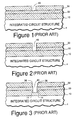
- Figures 1 is a fragmentary vertical cross-sectional view showing the prior art photolithographic formation of a pattern in the upper photoresist layer of a multilayer photoresist structure.
- Figures 2-4 are fragmentary vertical cross-sectional views sequentially illustrating the prior art practice of reproducing, in a lower photoresist layer, a pattern photolithographically formed in an upper photoresist layer.
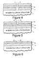
- Figures 5-8 are fragmentary vertical cross-sectional views sequentially illustrating one embodiment of the process of the invention for accurately reproducing, in a lower photoresist layer, a pattern photolithographically formed in an upper photoresist layer.
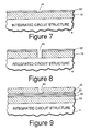
- Figures 9-13 are fragmentary vertical cross-sectional views sequentially illustrating another embodiment of the process of the invention for accurately reproducing, in a lower photoresist layer, a pattern photolithographically formed in an upper photoresist layer.
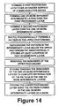
- Figure 14 is a flowsheet illustrating the process of the invention.
- the invention provides a process for accurately reproducing, in a lower photoresist mask, a pattern photolithographically formed in the upper photoresist layer of a multilayer photoresist having at least one layer of a different material formed in between the two photoresist layers, to form a mask which permits the accurate formation of a patterned layer on an uneven surface of a semiconductor wafer.
- the invention may find greatest utility at the present time in the construction of integrated circuit structures on silicon wafers, it should be noted that the invention may also be used in connection with other semiconductor wafers as well, including, but not limited to Group III-V type semiconductors such as, for example, gallium arsenide or indium arsenide wafers.
- Group III-V type semiconductors such as, for example, gallium arsenide or indium arsenide wafers.
- first photoresist layer 10 which may have a thickness ranging from about 1 micron to about 3 microns, is formed over the uneven surface of a semiconductor wafer which may have an integrated circuit structure previously formed in and on the surface of the wafer, resulting in the uneven or stepped surface.
- a different material such as an oxide of silicon, e.g., SiO2
- a second planarizing layer 30 of photoresist is formed over layer 20, and then photolithographically patterned to form openings such as opening 40.
- layer 20 which will be utilized in the practice of the process of the present invention, need not constitute oxide, but may instead, comprise any materials which may be etched independent of either of the photoresist layers as will be apparent below.
- layer 20 could comprise a metal layer such as aluminum, a polysilicon layer, or a silicon nitride layer, etc.
- intermediate layer 20 Other materials which could be used in intermediate layer 20 include refractory materials including tungsten, tungsten silicide, titanium, titanium silicide, titanium nitride, and titanium-tungsten; as well as compounds which include one or more group III or Group v elements such as gallium, indium, antimony, arsenic, boron, and phosphorus.
- the thickness of intermediate layer 20 may range from about 750-1500 Angstroms, and typically will be about 1000 Angstroms.
- the intermediate layer 20, which served as a stop for the photolithographic processing of upper layer 30, would have been completely etched through, using an anisotropic etch system with selectivity of the intermediate layer to the photoresist, using the pattern in upper photoresist mask layer 30, e.g., opening 40, as the mask for etching layer 20.
- intermediate layer 20 which will hereinafter be referred to as an oxide layer for purposes of illustration and not of limitation, is only partially etched through, as shown at 22 in Figure 5, using the mask pattern formed in upper photoresist layer 10 as the etch mask for an anisotropic etch such as a dry etch using a plasma.
- the anisotropic dry etch will preferably be carried out using a chemistry containing fluorocarbons such as, for example, CF4, CHF3, or C2F6 flowing into an etching chamber such as, for example, a single wafer etching chamber, at a rate within a range of from about 5 standard cubic centimeters/minute (sccm) to about 200 sccm and using a plasma at a power within a range of from about 50 Watts to about 500 Watts, and pressure from about 10 milliTorr to about 4 Torr.
- a chemistry containing fluorocarbons such as, for example, CF4, CHF3, or C2F6 flowing into an etching chamber
- an etching chamber such as, for example, a single wafer etching chamber
- a plasma at a power within a range of from about 50 Watts to about 500 Watts, and pressure from about 10 milliTorr to about 4 Torr.
- the etch chemistry When intermediate layer 20 constitutes another material, the etch chemistry will be changed accordingly.
- the etch chemistry when layer 20 comprises silicon nitride, the etch chemistry may also comprise CF4, CHF3, or C2F6; but when layer 20 comprises a metal layer such as aluminum, the etch chemistry may comprise, for example, BCl3, HCl, Cl2, SiCl4, or CCl4; and when layer 20 comprises polysilicon, the etch chemistry may comprise, for example, BCl3, Cl2, HCl, CCl4, Br2, or HBr.
- the flow rate of the etch chemistry may range from about 5 sccm to about 200 sccm, the plasma power level from about 50 to about 500 Watts, and the pressure from about 10 milliTorr to about 4 Torr (i.e., conditions similar to etching of an oxide layer; but when layer 20 comprises aluminum, the flow rate may range from about 5 sccm to about 100 sccm, the plasma power level from about 50 to about 300 Watts, and the pressure from about 1 milliTorr to about 1 Torr; and when layer 20 comprises polysilicon, the flow rate may range from about 5 sccm to about 100 sccm, the plasma power level from about 50 to about 300 Watts, and the pressure from about 1 milliTorr to about 1 Torr.
- Si3N4 silicon nitride
- the extent of the depth of the initial anisotropic etching of oxide layer 20, will vary from at least about 60% up to about 90%, i.e., leaving from about 10% to about 40% of the oxide layer remaining.
- the amount of oxide removed through opening 40 in upper photoresist layer 30 will range from about 70% to about 80%, i.e., leaving from about 20% to about 30% of the oxide thickness remaining.
- the minimum amount of at least about 60% is selected to ensure leaving an adequate thickness of oxide mask layer 20 over bottom photoresist layer 10 during a subsequent blanket etch step used to remove the remainder of the oxide exposed through opening 40, as will be described below.
- the maximum amount of oxide removed in this first step is selected to ensure that a sufficient amount of oxide will be left in opening 40 over underlying photoresist layer 10 as a protective layer so that bottom photoresist layer 10 will not be etched during the subsequent step of removing the remainder of upper photoresist layer 30.
- the etch chemistry may be changed to completely remove upper photoresist layer 30, as shown in Figure 6, using, for example, O2, CO, or N2O, at a flow rate of from about 50 to about 500 sccm at a pressure ranging from about 100 milliTorr to about 4 Torr and a plasma at a power level of from about 50 Watts to about 500 Watts to remove the remainder of upper photoresist layer 30.
- this particular step need not be an anisotropic etch, but conveniently will also be carried out as a dry etch in view of the location of the semiconductor wafer for other etch steps of the process which must be carried out under anisotropic etch conditions.
- the remaining oxide (or alternate intermediate material) in opening 40 is removed by a blanket oxide etch, again using appropriate etch chemistry, depending upon the material comprising layer 20, as previously described, e.g., such as a fluorocarbon as an etchant for an oxide layer.
- lower photoresist layer 10 may now be etched, utilizing an oxygen-containing chemistry, such as, for example, O2, CO, or N2O, and conditions optimal for anisotropic etching, i.e., a flow rate of from about 5 sccm to about 50 sccm, a power level of from about 50 Watts to about 300 Watts, and a pressure of from about 0.1 milliTorr to about 100 milliTorr, using oxide layer 20' as an etch mask, resulting in the structure shown in Figure 8.
- an oxygen-containing chemistry such as, for example, O2, CO, or N2O
- oxide layer 20' may be removed, if necessary or desired, using, for example, an oxide etch, and the patterned lower photoresist mask may be utilized in further conventional processing. It should be noted, however, that it may not be necessary to remove layer 20' since the material to be etched beneath lower photoresist layer 10 may constitute the same material as layer 20', e.g., an oxide layer. Furthermore, subsequent removal of lower photoresist layer 10, after completion of an etch of the layer below photoresist layer 10, will result in removal of any portions of layer 20' thereon.
- FIG. 9-13 another embodiment of the invention is shown which employs an additional intermediate layer 50 between intermediate layer 20 and lower photoresist layer 10, as shown in Figure 9 wherein the opening 40 is already shown as photolithographically formed in upper photoresist layer 30, as in the previous embodiment.
- the purpose of this additional intermediate layer is to provide an etch stop when opening 40 is being etched in intermediate layer 20.
- the use of such a second intermediate layer as an etch block eliminates the need to partially etch opening 40 in intermediate layer 20 and thus eliminates the need to carefully control the extent of the depth of the partial etch, as described in the previous embodiment.
- opening 40 may be anisotropically etched through the entire thickness of intermediate layer 20, using intermediate layer 50 as the etch stop for the etch system used to etch layer 20.
- second intermediate layer 50 will be referred to as an aluminum layer by way of illustration and not of limitation. However, it will be understood that any of the materials previously discussed as suitable for layer 20 may be utilized for layer 50 as long as layers 20 and 50 constitute different materials from that group.
- the thickness of second intermediate layer 50 may range from about 750-1500 Angstroms, and typically will be about 1000 Angstroms.
- upper photoresist layer 30 may be removed in the manner previously described resulting in the structure shown in Figure 11.
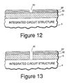
- Opening 40 is then etched through aluminum layer 50, as shown in Figure 12, using the previously formed opening 40 in oxide layer 20 as the etch mask for aluminum layer 50.
- Aluminum layer 50 may be either dry etched or wet etched.
- a chlorinated chemistry such as BCl3, Cl2, HCl, SiCl4, or CCl4, may be used for a plasma-assisted anisotropic dry etch, while an acid such as phosphoric acid, acetic acid, or nitric acid may be used for a wet etch.
- an acid such as phosphoric acid, acetic acid, or nitric acid may be used for a wet etch.
- the use of a dry etch will probably be preferred since the wafer will already be loaded into a dry etching apparatus to perform the mandatory anisotropic etching steps.
- opening 40 may be anisotropically etched in lower photoresist layer 10, using the oxide and aluminum intermediate layers as etch masks resulting in the structure shown in Figure 13. As in the previous embodiment, the intermediate layers may then be conventionally removed, if desired, and the lower photoresist mask used in further conventional processing.
- SiO2 silicon dioxide
- a pattern was then photolithographically formed in the upper photoresist by exposing the photoresist to a light pattern through a photolithography mask and then developing the exposed photoresist layer.
- the structure was then anisotropically etched while flowing 30 sccm of CF4 into the etch chamber at a pressure of about 50 milliTorr, and maintaining a plasma power of about 200 Watts, to etch the underlying oxide layer.
- the etch was continued until about 70 % of the oxide layer had been etched through the photolithographically formed openings in the upper photoresist layer.
- the etch chemistry was then changed to flow 200 sccm of O2 into the etch chamber at a pressure throttled to 500 milliTorr, while maintaining the same plasma power, to remove all of the upper layer of photoresist.
- the oxide etch was resumed until the lower photoresist layer was exposed through the openings formed in the oxide layer.
- the etch chemistry was then again changed by again flowing O2 into the etch chamber, at a flow rate of about 20 sccm and at a pressure of about 5 milliTorr, using a power level of about 100 Watts, to etch openings through the lower photoresist layer using the patterned oxide layer as a mask.
- the remainder of the oxide layer was then removed with an HF wet etch to permit examination of the quality of the resulting openings in the lower photoresist mask and comparison with the original photolithography mask used to pattern the upper photoresist layer.
- the pattern of the original photolithography mask was found to have been accurately reproduced in the lower photoresist layer with no evidence of bowing or unevenness of the sidewalls of the openings in the resulting photoresist mask.
- another semiconductor wafer also having integrated circuit structure already formed thereon, resulting in an uneven surface, was also coated with a first layer of a photoresist which was spun on to an average thickness of about 2 microns.
- a first intermediate layer of aluminum having an average thickness of about 1000 Angstroms was then formed over the photoresist layer.
- a silicon dioxide (SiO2) layer having an average thickness of about 1000 Angstroms was deposited over the aluminum layer.
- a second photoresist layer having an average thickness of about micron, was then spun on over the oxide layer, resulting in a substantially planarized surface on the wafer.
- Example I a pattern was then photolithographically formed in the upper photoresist layer by exposing the layer to a light pattern through a photolithography mask and then developing the exposed photoresist layer.
- the structure was then anisotropically etched while flowing 30 sccm of CF4 into the etch chamber at a pressure of about 50 milliTorr and maintaining a plasma power of about 200 Watts to etch openings through the underlying oxide layer, using the formed openings in the upper photoresist layer as a mask, and using the underlying aluminum layer as an etch stop.
- the etch chemistry was then changed to flow 200 sccm of O2 into the etch chamber at about 500 milliTorr, while maintaining the same plasma power, to remove all of the upper layer of photoresist.
- the etch chemistry was changed to flow 10 sccm of BCl3 and 25 sccm of Cl2 at a pressure of about 100 milliTorr and a power level of about 100 Watts, to etch the portions of the aluminum layer exposed through the openings formed in the oxide layer.
- the etch chemistry was again changed by again flowing O2 into the etch chamber to etch openings through the lower photoresist layer using the patterned oxide and aluminum layers as the mask.
- the remainder of the oxide layer was then removed with an HF wet etch (again for examination purposes) and the underlying aluminum mask was also removed.
- the resulting openings in this lower photoresist mask were then examined and also compared with the original photolithography mask.
- the pattern of the original photolithography mask was again found to have been accurately reproduced in the lower photoresist layer with no evidence of bowing or unevenness of the sidewalls of the openings in the resulting photoresist mask.
- the initial openings photolithographically formed in upper photoresist layer 30 may be accurately reproduced in lower photoresist layer 10 resulting in the accurate and precise patterning of the uneven surface of a semiconductor wafer having integrated circuit structure such as raised lines, etc., already formed thereon.
- the process of the invention eliminates the problem of faceting of the corners of the mask opening formed in the upper photoresist layer, thereby eliminating the formation of bowed sidewalls in the opening formed in the lower photoresist layer.
- the process of the invention also eliminates the problem of changes in the photoresist load during the etching of the opening in the lower photoresist layer since both photoresist layers are never simultaneously etched.
Landscapes
- Engineering & Computer Science (AREA)
- Physics & Mathematics (AREA)
- General Physics & Mathematics (AREA)
- Architecture (AREA)
- Structural Engineering (AREA)
- Manufacturing & Machinery (AREA)
- Condensed Matter Physics & Semiconductors (AREA)
- Computer Hardware Design (AREA)
- Microelectronics & Electronic Packaging (AREA)
- Power Engineering (AREA)
- Drying Of Semiconductors (AREA)
- Photosensitive Polymer And Photoresist Processing (AREA)
- Exposure Of Semiconductors, Excluding Electron Or Ion Beam Exposure (AREA)
Abstract
Description
- This invention relates to an improved process for forming a mask on an uneven surface of a semiconductor wafer using multilayers of photoresist. More particularly, this invention relates to an improved process for etching a multilayer photoresist mask structure formed on an uneven surface of a semiconductor wafer which will minimize feature undercutting of the lower portions of the mask and also provide even loading of the photoresist during etching.
- In the preparation of photoresist masks over stepped or uneven surfaces of a semiconductor wafer, it is known that focus (optically-related) problems can occur in the photolithographic transfer of the pattern from the photolithography mask to the photoresist layer when the photoresist layer is not flat. This results in the lack of control of critical dimensions of the features which define the performance of an integrated circuit.
- Therefore, when forming a photoresist mask over an uneven surface on a semiconductor wafer in the prior art, e.g., a wafer having already formed thereon integrated circuit structure including raised lines or trenches or the like, it has become the practice to use a multilayer photoresist structure.
- As shown in the prior art photolithography step of Figure 1, a planarizing
photoresist layer 10 is first formed (spun) over anintegrated circuit structure 4 comprising the uneven surface portion of a semiconductor wafer. Anintermediate layer 20, which may comprise an oxide such as a spin on glass (SOG) or a CVD formed silicon dioxide glass, is deposited over firstphotoresist layer 10 and then a second imaging layer ofphotoresist 30 is formed overoxide layer 20 to provide a level photoresist surface onto which may be projected a light image of the desired pattern from a photolithographic mask, using standard photolithography techniques. -
Opening 40 is then photolithographically formed in upperphotoresist mask layer 30, as shown in Figure 1, by optical projection of a light pattern ontophotoresist layer 30, followed by development of the photoresist as is well known to those skilled in the art. - While the foregoing practice solves the photolithography problem of attempting to form a light pattern on an uneven surface of a photoresist layer, there still remains the problem of accurately transferring to lower
photoresist layer 10 the pattern photolithographically formed in upperphotoresist layer 30. - Figures 2-4 sequentially illustrate the prior art practice of forming in lower
photoresist layer 10 the pattern photolithographically formed in upperphotoresist layer 30. - As shown in Figure 2, the initial step in the prior art, following the photolithography step, was to anisotropically etch the
oxide layer 20 in between the upper and lower photoresist layers throughopening 40 formed in upperphotoresist layer 30, using an appropriate oxide etch chemistry, thereby exposing that portion of the surface of underlying lowerphotoresist layer 10 through opening 40. - The etch chemistry was then changed to a photoresist etch chemistry to anisotropically etch an opening through lower
photoresist mask layer 10, using opening 40 formed in upperphotoresist mask layer 30 andoxide layer 20 as a mask, as shown in Figures 3 and 4. - However, as seen in Figures 3 and 4, two problems were encountered in the prior art with this process. First of all, when the etch chemistry is changed to etch photoresist, the exposed portion of lower
photoresist layer 10 is etched through opening 40 simultaneous with the blanket etching of the entire surface of upperphotoresist layer 30. However, when upperphotoresist layer 30 has been completely removed, the etch loading on the system drastically changes, since only the relatively small surface area ofphotoresist layer 10 exposed by opening 40 (as well as other similar openings in oxide layer 20) is now being etched. This results in problems of control of the etch rate. - Additional problems which were encountered in the prior art using the above procedures included detection of the process end (by emission spectroscopy) due to the increase in etch/rate and the signal intensity change when
layers 30 clears. Also, the change in gas phase composition, when changing the etch chemistry during the process, affects the process results, e.g., the feature profile of the resulting integrated circuit structure. - Furthermore, it will also be noted in Figure 3 that during the anisotropic blanket etching of upper
photoresist layer 30, faceting of the edge ofphotoresist layer 30 occurs at the corners of opening 40, as shown at 36. This, in turn, results in deflection or reflection of the etch ions from these surfaces to strike the sidewalls of lowerphotoresist layer 10 at 14, during the anisotropic photoresist etch step, causing a bowing effect in the sidewalls of the opening 40 being etched in lowerphotoresist layer 10. When this occurs, a true image of the pattern photolithographically formed in upperphotoresist layer 30 will not be reproduced precisely in lowerphotoresist layer 10, thus defeating the whole purpose of using a multilayer photoresist mask. - It is, therefore, an object of this invention to provide a process for forming an etch mask over the uneven surface of a semiconductor wafer using a multilayer photoresist wherein a mask pattern photolithographically formed in the upper photoresist layer may be accurately reproduced in the lower photoresist layer.
- It is another object of this invention to provide a process for forming an etch mask over the uneven surface of a semiconductor wafer using a multilayer photoresist having at least one layer of a different material in between the photoresist layers wherein a mask pattern photolithographically formed in the upper photoresist layer may be accurately reproduced in the lower photoresist layer by completely removing the upper layer of photoresist before anisotropically etching the lower layer of photoresist.
- It is still another object of this invention to provide a process for forming an etch mask over the uneven surface of a semiconductor wafer using a multilayer photoresist having at least one layer of a different material in between the photoresist layers wherein a mask pattern photolithographically formed in the upper photoresist layer may be accurately reproduced in the lower photoresist layer by reproducing, in the layer of different material, the mask pattern photolithographically formed in the upper layer of photoresist, and then completely removing the upper layer of photoresist before anisotropically etching the lower layer of photoresist.
- It is yet another object of this invention to provide a process for forming an etch mask over the uneven surface of a semiconductor wafer using a multilayer photoresist having at least one layer of a different material in between the photoresist layers wherein a mask pattern photolithographically formed in the upper photoresist layer may be accurately reproduced in the lower photoresist layer by reproducing, in the layer of different material, the mask pattern photolithographically formed in the upper layer of photoresist, by partially etching anisotropically the layer of different material and then completely removing the upper layer of photoresist before anisotropically etching through the remainder of the layer of different material and before anisotropically etching the lower layer of photoresist.
- It is a further object of this invention to provide a process for forming an etch mask over the uneven surface of a semiconductor wafer using a multilayer photoresist having at least two layers of different materials in between the photoresist layers wherein a mask pattern photolithographically formed in the upper photoresist layer may be accurately reproduced in the lower photoresist layer by reproducing, in the upper layer of different material, the mask pattern photolithographically formed in the upper layer of photoresist, by anisotropically etching through the upper layer of different material, using the lower layer of different material as an etch stop, and then completely removing the upper layer of photoresist before etching through the lower layer of different material and before anisotropically etching the lower layer of photoresist.
- These and other objects of the invention will be apparent from the following description and accompanying drawings.
- Figures 1 is a fragmentary vertical cross-sectional view showing the prior art photolithographic formation of a pattern in the upper photoresist layer of a multilayer photoresist structure.
- Figures 2-4 are fragmentary vertical cross-sectional views sequentially illustrating the prior art practice of reproducing, in a lower photoresist layer, a pattern photolithographically formed in an upper photoresist layer.
- Figures 5-8 are fragmentary vertical cross-sectional views sequentially illustrating one embodiment of the process of the invention for accurately reproducing, in a lower photoresist layer, a pattern photolithographically formed in an upper photoresist layer.
- Figures 9-13 are fragmentary vertical cross-sectional views sequentially illustrating another embodiment of the process of the invention for accurately reproducing, in a lower photoresist layer, a pattern photolithographically formed in an upper photoresist layer.
- Figure 14 is a flowsheet illustrating the process of the invention.
- The invention provides a process for accurately reproducing, in a lower photoresist mask, a pattern photolithographically formed in the upper photoresist layer of a multilayer photoresist having at least one layer of a different material formed in between the two photoresist layers, to form a mask which permits the accurate formation of a patterned layer on an uneven surface of a semiconductor wafer.
- While the invention may find greatest utility at the present time in the construction of integrated circuit structures on silicon wafers, it should be noted that the invention may also be used in connection with other semiconductor wafers as well, including, but not limited to Group III-V type semiconductors such as, for example, gallium arsenide or indium arsenide wafers.
- Turning now to Figures 5-8, the sequential steps of the first embodiment of the process are illustrated. In this embodiment, the prior art structure shown in Figure 1 serves as the starting point for the process of the invention. As previously described above, first
photoresist layer 10, which may have a thickness ranging from about 1 micron to about 3 microns, is formed over the uneven surface of a semiconductor wafer which may have an integrated circuit structure previously formed in and on the surface of the wafer, resulting in the uneven or stepped surface. - A
layer 20 of a different material such as an oxide of silicon, e.g., SiO₂, is formed overlayer 10 and a second planarizinglayer 30 of photoresist is formed overlayer 20, and then photolithographically patterned to form openings such as opening 40. - While the structure and processing described so far constitutes the prior art, it should, nevertheless, be mentioned at this point that
layer 20, which will be utilized in the practice of the process of the present invention, need not constitute oxide, but may instead, comprise any materials which may be etched independent of either of the photoresist layers as will be apparent below. Thuslayer 20 could comprise a metal layer such as aluminum, a polysilicon layer, or a silicon nitride layer, etc. Other materials which could be used inintermediate layer 20 include refractory materials including tungsten, tungsten silicide, titanium, titanium silicide, titanium nitride, and titanium-tungsten; as well as compounds which include one or more group III or Group v elements such as gallium, indium, antimony, arsenic, boron, and phosphorus. The thickness ofintermediate layer 20 may range from about 750-1500 Angstroms, and typically will be about 1000 Angstroms. - At this point, in the prior art, the
intermediate layer 20, which served as a stop for the photolithographic processing ofupper layer 30, would have been completely etched through, using an anisotropic etch system with selectivity of the intermediate layer to the photoresist, using the pattern in upperphotoresist mask layer 30, e.g., opening 40, as the mask foretching layer 20. - However, instead, in accordance with this embodiment of the process of the invention,
intermediate layer 20, which will hereinafter be referred to as an oxide layer for purposes of illustration and not of limitation, is only partially etched through, as shown at 22 in Figure 5, using the mask pattern formed in upperphotoresist layer 10 as the etch mask for an anisotropic etch such as a dry etch using a plasma. - When
intermediate layer 20 is an oxide layer the anisotropic dry etch will preferably be carried out using a chemistry containing fluorocarbons such as, for example, CF₄, CHF₃, or C₂F₆ flowing into an etching chamber such as, for example, a single wafer etching chamber, at a rate within a range of from about 5 standard cubic centimeters/minute (sccm) to about 200 sccm and using a plasma at a power within a range of from about 50 Watts to about 500 Watts, and pressure from about 10 milliTorr to about 4 Torr. It will be understood, of course, that the above flow rates would have to be appropriately scaled upward for multiple wafer etching chambers. - When
intermediate layer 20 constitutes another material, the etch chemistry will be changed accordingly. For example, whenlayer 20 comprises silicon nitride, the etch chemistry may also comprise CF₄, CHF₃, or C₂F₆; but whenlayer 20 comprises a metal layer such as aluminum, the etch chemistry may comprise, for example, BCl₃, HCl, Cl₂, SiCl₄, or CCl₄; and whenlayer 20 comprises polysilicon, the etch chemistry may comprise, for example, BCl₃, Cl₂, HCl, CCl₄, Br₂, or HBr. - The flow rates, power levels, and pressure range will also vary, depending upon the type of material which constitutes
layer 20. For example, whenlayer 20 comprises a silicon nitride (Si₃N₄) layer, the flow rate of the etch chemistry may range from about 5 sccm to about 200 sccm, the plasma power level from about 50 to about 500 Watts, and the pressure from about 10 milliTorr to about 4 Torr (i.e., conditions similar to etching of an oxide layer; but whenlayer 20 comprises aluminum, the flow rate may range from about 5 sccm to about 100 sccm, the plasma power level from about 50 to about 300 Watts, and the pressure from about 1 milliTorr to about 1 Torr; and whenlayer 20 comprises polysilicon, the flow rate may range from about 5 sccm to about 100 sccm, the plasma power level from about 50 to about 300 Watts, and the pressure from about 1 milliTorr to about 1 Torr. - The extent of the depth of the initial anisotropic etching of
oxide layer 20, will vary from at least about 60% up to about 90%, i.e., leaving from about 10% to about 40% of the oxide layer remaining. Preferably the amount of oxide removed through opening 40 in upperphotoresist layer 30 will range from about 70% to about 80%, i.e., leaving from about 20% to about 30% of the oxide thickness remaining. - The minimum amount of at least about 60% is selected to ensure leaving an adequate thickness of
oxide mask layer 20 over bottomphotoresist layer 10 during a subsequent blanket etch step used to remove the remainder of the oxide exposed throughopening 40, as will be described below. The maximum amount of oxide removed in this first step is selected to ensure that a sufficient amount of oxide will be left in opening 40 over underlyingphotoresist layer 10 as a protective layer so that bottomphotoresist layer 10 will not be etched during the subsequent step of removing the remainder of upperphotoresist layer 30. - After the partial anisotropic etching of
oxide layer 30 through upperphotoresist mask layer 30, the etch chemistry may be changed to completely remove upperphotoresist layer 30, as shown in Figure 6, using, for example, O₂, CO, or N₂O, at a flow rate of from about 50 to about 500 sccm at a pressure ranging from about 100 milliTorr to about 4 Torr and a plasma at a power level of from about 50 Watts to about 500 Watts to remove the remainder of upperphotoresist layer 30. It should be noted that this particular step need not be an anisotropic etch, but conveniently will also be carried out as a dry etch in view of the location of the semiconductor wafer for other etch steps of the process which must be carried out under anisotropic etch conditions. - After the removal of upper
photoresist layer 30, the remaining oxide (or alternate intermediate material) inopening 40 is removed by a blanket oxide etch, again using appropriate etch chemistry, depending upon thematerial comprising layer 20, as previously described, e.g., such as a fluorocarbon as an etchant for an oxide layer. - This blanket etch also results in the thinning of the remainder of
layer 20, as shown in Figure 7, in which thethinned layer 20 is now designated as 20'. However, if the depth of the initial partial etch of opening 40 inlayer 20 was deep enough, as previously discussed, removal of the remaining oxide in opening 40 should not result in the removal of an excessive amount of the remainder of oxide layer 20'. - With the removal of the remainder of
intermediate layer 20 from opening 40,lower photoresist layer 10 may now be etched, utilizing an oxygen-containing chemistry, such as, for example, O₂, CO, or N₂O, and conditions optimal for anisotropic etching, i.e., a flow rate of from about 5 sccm to about 50 sccm, a power level of from about 50 Watts to about 300 Watts, and a pressure of from about 0.1 milliTorr to about 100 milliTorr, using oxide layer 20' as an etch mask, resulting in the structure shown in Figure 8. - At this point the remainder of oxide layer 20' may be removed, if necessary or desired, using, for example, an oxide etch, and the patterned lower photoresist mask may be utilized in further conventional processing. It should be noted, however, that it may not be necessary to remove layer 20' since the material to be etched beneath
lower photoresist layer 10 may constitute the same material as layer 20', e.g., an oxide layer. Furthermore, subsequent removal oflower photoresist layer 10, after completion of an etch of the layer belowphotoresist layer 10, will result in removal of any portions of layer 20' thereon. - It will be nosed that since
photoresist layer 10 is etched only through layer 20', and not throughupper photoresist layer 30 as well, as in the prior art process shown in Figures 2-4, the walls of the opening etched inlower photoresist layer 10 are straight, unlike the bowed walls of Figure 4. - Furthermore, not only has the problem of the faceted corners in the upper photoresist layer (shown in prior art Figure 3) been minimized by the process of the invention, but the prior art problem of change in photoresist load during etching has also been eliminated since the upper and lower photoresist layers are never etched simultaneously as in the prior art process.
- Turning now to Figures 9-13, another embodiment of the invention is shown which employs an additional
intermediate layer 50 betweenintermediate layer 20 andlower photoresist layer 10, as shown in Figure 9 wherein theopening 40 is already shown as photolithographically formed inupper photoresist layer 30, as in the previous embodiment. The purpose of this additional intermediate layer is to provide an etch stop when opening 40 is being etched inintermediate layer 20. The use of such a second intermediate layer as an etch block eliminates the need to partially etch opening 40 inintermediate layer 20 and thus eliminates the need to carefully control the extent of the depth of the partial etch, as described in the previous embodiment. - Instead, as shown in Figure 10, in this embodiment of the process, opening 40 may be anisotropically etched through the entire thickness of
intermediate layer 20, usingintermediate layer 50 as the etch stop for the etch system used to etchlayer 20. - In view of this function of
layer 50, it is important thatlayer 50 comprise a material different from either the photoresist material used inlayers intermediate layer 20. In the illustrated embodiment, secondintermediate layer 50 will be referred to as an aluminum layer by way of illustration and not of limitation. However, it will be understood that any of the materials previously discussed as suitable forlayer 20 may be utilized forlayer 50 as long aslayers intermediate layer 50 may range from about 750-1500 Angstroms, and typically will be about 1000 Angstroms. - After opening 40 has been anisotropically etched in
oxide layer 20,upper photoresist layer 30 may be removed in the manner previously described resulting in the structure shown in Figure 11. -
Opening 40 is then etched throughaluminum layer 50, as shown in Figure 12, using the previously formedopening 40 inoxide layer 20 as the etch mask foraluminum layer 50.Aluminum layer 50 may be either dry etched or wet etched. A chlorinated chemistry, such as BCl₃, Cl₂, HCl, SiCl₄, or CCl₄, may be used for a plasma-assisted anisotropic dry etch, while an acid such as phosphoric acid, acetic acid, or nitric acid may be used for a wet etch. As in the previously described embodiment, the use of a dry etch will probably be preferred since the wafer will already be loaded into a dry etching apparatus to perform the mandatory anisotropic etching steps. - After forming
opening 40 in lowerintermediate layer 50, opening 40 may be anisotropically etched inlower photoresist layer 10, using the oxide and aluminum intermediate layers as etch masks resulting in the structure shown in Figure 13. As in the previous embodiment, the intermediate layers may then be conventionally removed, if desired, and the lower photoresist mask used in further conventional processing. - The following examples will serve to further illustrate the process of the invention.
- A semiconductor wafer having integrated circuit structure already formed thereon, resulting in an uneven surface, was coated with a first layer of a photoresist which was spun on to an average thickness of about 2 microns. A silicon dioxide (SiO₂) layer having an average thickness of about 1000 Angstroms was deposited over the photoresist layer and then a second photoresist layer, having an average thickness of about 1 micron, was spun on over the oxide layer, resulting in a substantially planarized surface on the wafer.
- A pattern was then photolithographically formed in the upper photoresist by exposing the photoresist to a light pattern through a photolithography mask and then developing the exposed photoresist layer.
- The structure was then anisotropically etched while flowing 30 sccm of CF₄ into the etch chamber at a pressure of about 50 milliTorr, and maintaining a plasma power of about 200 Watts, to etch the underlying oxide layer. The etch was continued until about 70 % of the oxide layer had been etched through the photolithographically formed openings in the upper photoresist layer. The etch chemistry was then changed to flow 200 sccm of O₂ into the etch chamber at a pressure throttled to 500 milliTorr, while maintaining the same plasma power, to remove all of the upper layer of photoresist.
- After removal of all of the upper layer of photoresist, the oxide etch was resumed until the lower photoresist layer was exposed through the openings formed in the oxide layer. The etch chemistry was then again changed by again flowing O₂ into the etch chamber, at a flow rate of about 20 sccm and at a pressure of about 5 milliTorr, using a power level of about 100 Watts, to etch openings through the lower photoresist layer using the patterned oxide layer as a mask. The remainder of the oxide layer was then removed with an HF wet etch to permit examination of the quality of the resulting openings in the lower photoresist mask and comparison with the original photolithography mask used to pattern the upper photoresist layer. The pattern of the original photolithography mask was found to have been accurately reproduced in the lower photoresist layer with no evidence of bowing or unevenness of the sidewalls of the openings in the resulting photoresist mask.
- To illustrate the second embodiment of the invention, another semiconductor wafer, also having integrated circuit structure already formed thereon, resulting in an uneven surface, was also coated with a first layer of a photoresist which was spun on to an average thickness of about 2 microns. A first intermediate layer of aluminum, having an average thickness of about 1000 Angstroms was then formed over the photoresist layer. A silicon dioxide (SiO₂) layer having an average thickness of about 1000 Angstroms was deposited over the aluminum layer. A second photoresist layer, having an average thickness of about micron, was then spun on over the oxide layer, resulting in a substantially planarized surface on the wafer.
- As in Example I, a pattern was then photolithographically formed in the upper photoresist layer by exposing the layer to a light pattern through a photolithography mask and then developing the exposed photoresist layer.
- The structure was then anisotropically etched while flowing 30 sccm of CF₄ into the etch chamber at a pressure of about 50 milliTorr and maintaining a plasma power of about 200 Watts to etch openings through the underlying oxide layer, using the formed openings in the upper photoresist layer as a mask, and using the underlying aluminum layer as an etch stop. The etch chemistry was then changed to flow 200 sccm of O₂ into the etch chamber at about 500 milliTorr, while maintaining the same plasma power, to remove all of the upper layer of photoresist.
- After removal of all of the upper layer of photoresist, the etch chemistry was changed to flow 10 sccm of BCl₃ and 25 sccm of Cl₂ at a pressure of about 100 milliTorr and a power level of about 100 Watts, to etch the portions of the aluminum layer exposed through the openings formed in the oxide layer. When the aluminum was etched through, exposing the lower photoresist layer, the etch chemistry was again changed by again flowing O₂ into the etch chamber to etch openings through the lower photoresist layer using the patterned oxide and aluminum layers as the mask.
- The remainder of the oxide layer was then removed with an HF wet etch (again for examination purposes) and the underlying aluminum mask was also removed. The resulting openings in this lower photoresist mask were then examined and also compared with the original photolithography mask. The pattern of the original photolithography mask was again found to have been accurately reproduced in the lower photoresist layer with no evidence of bowing or unevenness of the sidewalls of the openings in the resulting photoresist mask.
- Thus, in either embodiment of the process of the invention, the initial openings photolithographically formed in
upper photoresist layer 30 may be accurately reproduced inlower photoresist layer 10 resulting in the accurate and precise patterning of the uneven surface of a semiconductor wafer having integrated circuit structure such as raised lines, etc., already formed thereon. The process of the invention eliminates the problem of faceting of the corners of the mask opening formed in the upper photoresist layer, thereby eliminating the formation of bowed sidewalls in the opening formed in the lower photoresist layer. The process of the invention also eliminates the problem of changes in the photoresist load during the etching of the opening in the lower photoresist layer since both photoresist layers are never simultaneously etched.
Claims (13)
- A process for forming an etch mask over the uneven surface of a semiconductor wafer using a multilayer photoresist wherein a mask pattern photolithographically formed in the upper photoresist layer may be accurately reproduced in the lower photoresist layer
characterized bya) forming a first photoresist layer (10) on the surface of a semiconductor wafer;b) forming one or more intermediate layers (20; 50) over said first photoresist layer (10);c) forming a second photoresist layer (30) over said one or more intermediate layers (20; 50) on said wafer;d) photolithographically forming a pattern in said second photoresist layer (30);e) reproducing said pattern in said one or more intermediate layers (20; 50) below said second photoresist layer (30);f) removing the remainder of said upper photoresist layer (30); andg) reproducing said pattern in said first photoresist layer (10) using said pattern formed in said one or more intermediate layers (20; 50) as a mask;
whereby a mask pattern photolithographically formed in said second photoresist layer (30) may be accurately reproduced in said first photoresist layer (10). - The process of claim 1
wherein said step of reproducing said pattern in said one or more intermediate layers (20; 50) below said second photoresist layer (30) further comprises anisotropically etching said one or more intermediate layers (20; 50). - The process of claim 1
wherein a single intermediate layer (20) is used and said step of reproducing said pattern in said intermediate layer (20) below said second photoresist layer (30) further comprises anisotropically etching partially through said intermediate layer (20). - The process of claim 3
wherein said step of reproducing said pattern in said intermediate layer below said second photoresist layer by anisotropically etching partially through said intermediate layer further comprises anisotropically etching through from about 60 to about 90%, preferably from about 80 to about 80% of the thickness of said intermediate layer (20). - The process of claim 3 or 4
including the further step of anisotropically etching through the remainder of said intermediate layer (20) after said step of removing said second layer (30) of photoresist. - The process of any of the preceding claims
wherein said intermediate layer (20) is selected from the class consisting of silicon dioxide, silicon nitride, polysilicon and aluminum. - The process of any of claims 1 to 5
wherein said intermediate layer (20) comprises a refractory material selected from the class consisting of tungsten, tungsten silicide, titanium, titanium silicide, titanium nitride and titanium-tungsten. - The process of any of claims 1 to 5
wherein said intermediate layer (20) comprises a Group III or Group V compound selected from the class consisting of a gallium compound, an indium compound, an antimony compound, an arsenic compound, a boron compound and a phosphorous compound. - The process of claim 1
wherein said step of forming one or more intermediate layers over said first photoresist layer (10) further comprises forming upper and lower intermediate layers (20; 50) of different materials over said first photoresist layer (10) and said step of reproducing said pattern in the intermediate layer below said second photoresist layer further comprises anisotropically etching the upper intermediate layer (20) using the lower intermediate layer (50) as an etch stop. - The process of claim 9
including the further step of etching said lower intermediate layer (50), after said step of removing the remainder of said upper photoresist layer (30), using said pattern etched in said upper intermediate layer (20) as an etch mask. - The process of claim 9 or 10
wherein said upper intermediate layer (20) is selected from the class consisting of silicon dioxide, silicon nitride, polysilicon, aluminum, tungsten, tungsten silicide, titanium, titanium silicide, titanium nitride, titanium-tungsten, a gallium compound, an indium compound, an antimony compound, an arsenic compound, a boron compound and a phosphorous compound; and said lower intermediate layer (50) comprises another material in said class. - The process of claim 9 or 10
wherein one of said intermediate layers (50) comprises aluminum and the other of said intermediate layers (20) comprises silicon dioxide. - The process of any of the preceding claims
including the further step of removing said one or more intermediate layers (20; 50) after reproducing said pattern in said first photoresist layer (10).
Applications Claiming Priority (2)
| Application Number | Priority Date | Filing Date | Title |
|---|---|---|---|
| US07/485,331 US5126231A (en) | 1990-02-26 | 1990-02-26 | Process for multi-layer photoresist etching with minimal feature undercut and unchanging photoresist load during etch |
| US485331 | 1990-02-26 |
Publications (3)
| Publication Number | Publication Date |
|---|---|
| EP0444531A2 true EP0444531A2 (en) | 1991-09-04 |
| EP0444531A3 EP0444531A3 (en) | 1993-06-16 |
| EP0444531B1 EP0444531B1 (en) | 1997-06-11 |
Family
ID=23927742
Family Applications (1)
| Application Number | Title | Priority Date | Filing Date |
|---|---|---|---|
| EP91102541A Expired - Lifetime EP0444531B1 (en) | 1990-02-26 | 1991-02-21 | Process for multi-layer photoresist etching with minimal feature undercut and unchanging photoresist load during etch |
Country Status (5)
| Country | Link |
|---|---|
| US (1) | US5126231A (en) |
| EP (1) | EP0444531B1 (en) |
| JP (1) | JP2593586B2 (en) |
| KR (1) | KR100216315B1 (en) |
| DE (1) | DE69126455T2 (en) |
Families Citing this family (71)
| Publication number | Priority date | Publication date | Assignee | Title |
|---|---|---|---|---|
| US5320934A (en) * | 1991-06-28 | 1994-06-14 | Misium George R | Bilayer photolithographic process |
| US5323047A (en) * | 1992-01-31 | 1994-06-21 | Sgs-Thomson Microelectronics, Inc. | Structure formed by a method of patterning a submicron semiconductor layer |
| JP2910382B2 (en) * | 1992-03-09 | 1999-06-23 | 日本電気株式会社 | Method for manufacturing semiconductor device |
| US5326727A (en) * | 1992-12-30 | 1994-07-05 | At&T Bell Laboratories | Method for integrated circuit fabrication including linewidth control during etching |
| US5770350A (en) * | 1993-11-09 | 1998-06-23 | Lg Semicon Co. Ltd. | Method for forming pattern using multilayer resist |
| US5587090A (en) * | 1994-04-04 | 1996-12-24 | Texas Instruments Incorporated | Multiple level mask for patterning of ceramic materials |
| US5506172A (en) * | 1994-08-29 | 1996-04-09 | Micron Technology, Inc. | Semiconductor processing method of forming an electrical interconnection between an outer layer and an inner layer |
| US5596226A (en) * | 1994-09-06 | 1997-01-21 | International Business Machines Corporation | Semiconductor chip having a chip metal layer and a transfer metal and corresponding electronic module |
| US6740573B2 (en) * | 1995-02-17 | 2004-05-25 | Micron Technology, Inc. | Method for forming an integrated circuit interconnect using a dual poly process |
| KR0156316B1 (en) * | 1995-09-13 | 1998-12-01 | 김광호 | Patterning method of semiconductor device |
| KR100223325B1 (en) * | 1995-12-15 | 1999-10-15 | 김영환 | Method for manufacturing fine pattern of semiconductor device |
| KR100206597B1 (en) * | 1995-12-29 | 1999-07-01 | 김영환 | Fine-patterning method of semiconductor device |
| KR100394762B1 (en) * | 1996-02-13 | 2003-11-20 | 주식회사 엘지생활건강 | Concentrated powdery detergent composition with excellent long period storage stability |
| US5976986A (en) * | 1996-08-06 | 1999-11-02 | International Business Machines Corp. | Low pressure and low power C12 /HC1 process for sub-micron metal etching |
| US6054384A (en) * | 1998-05-19 | 2000-04-25 | Advanced Micro Devices, Inc. | Use of hard masks during etching of openings in integrated circuits for high etch selectivity |
| US6269533B2 (en) * | 1999-02-23 | 2001-08-07 | Advanced Research Corporation | Method of making a patterned magnetic recording head |
| US20030093894A1 (en) * | 1999-02-23 | 2003-05-22 | Dugas Matthew P. | Double layer patterning and technique for making a magnetic recording head |
| US6496328B1 (en) | 1999-12-30 | 2002-12-17 | Advanced Research Corporation | Low inductance, ferrite sub-gap substrate structure for surface film magnetic recording heads |
| TW444274B (en) * | 2000-03-23 | 2001-07-01 | Mosel Vitelic Inc | Improvement method for dishing effect in the polysilicon film deposited on the trench |
| EP1229390A4 (en) * | 2000-06-22 | 2004-06-02 | Toray Industries | Positive type radiation-sensitive composition and process for producing pattern with the same |
| TW479323B (en) * | 2000-10-26 | 2002-03-11 | United Microelectronics Corp | Manufacturing method of dual damascene |
| US6409312B1 (en) | 2001-03-27 | 2002-06-25 | Lexmark International, Inc. | Ink jet printer nozzle plate and process therefor |
| JP3830777B2 (en) * | 2001-06-14 | 2006-10-11 | 富士通株式会社 | Manufacturing method of semiconductor device |
| US6811959B2 (en) | 2002-03-04 | 2004-11-02 | International Business Machines Corporation | Hardmask/barrier layer for dry etching chrome films and improving post develop resist profiles on photomasks |
| US6872506B2 (en) * | 2002-06-25 | 2005-03-29 | Brewer Science Inc. | Wet-developable anti-reflective compositions |
| US6740469B2 (en) | 2002-06-25 | 2004-05-25 | Brewer Science Inc. | Developer-soluble metal alkoxide coatings for microelectronic applications |
| US7507783B2 (en) * | 2003-02-24 | 2009-03-24 | Brewer Science Inc. | Thermally curable middle layer comprising polyhedral oligomeric silsesouioxanes for 193-nm trilayer resist process |
| US7667238B2 (en) * | 2003-04-15 | 2010-02-23 | Luminus Devices, Inc. | Light emitting devices for liquid crystal displays |
| US7105861B2 (en) * | 2003-04-15 | 2006-09-12 | Luminus Devices, Inc. | Electronic device contact structures |
| US7521854B2 (en) * | 2003-04-15 | 2009-04-21 | Luminus Devices, Inc. | Patterned light emitting devices and extraction efficiencies related to the same |
| US7084434B2 (en) * | 2003-04-15 | 2006-08-01 | Luminus Devices, Inc. | Uniform color phosphor-coated light-emitting diode |
| US7166871B2 (en) * | 2003-04-15 | 2007-01-23 | Luminus Devices, Inc. | Light emitting systems |
| US7074631B2 (en) * | 2003-04-15 | 2006-07-11 | Luminus Devices, Inc. | Light emitting device methods |
| US7211831B2 (en) * | 2003-04-15 | 2007-05-01 | Luminus Devices, Inc. | Light emitting device with patterned surfaces |
| US7083993B2 (en) * | 2003-04-15 | 2006-08-01 | Luminus Devices, Inc. | Methods of making multi-layer light emitting devices |
| US20040259279A1 (en) * | 2003-04-15 | 2004-12-23 | Erchak Alexei A. | Light emitting device methods |
| US6831302B2 (en) * | 2003-04-15 | 2004-12-14 | Luminus Devices, Inc. | Light emitting devices with improved extraction efficiency |
| US7098589B2 (en) * | 2003-04-15 | 2006-08-29 | Luminus Devices, Inc. | Light emitting devices with high light collimation |
| US7262550B2 (en) * | 2003-04-15 | 2007-08-28 | Luminus Devices, Inc. | Light emitting diode utilizing a physical pattern |
| US7274043B2 (en) * | 2003-04-15 | 2007-09-25 | Luminus Devices, Inc. | Light emitting diode systems |
| US7344903B2 (en) * | 2003-09-17 | 2008-03-18 | Luminus Devices, Inc. | Light emitting device processes |
| US6916697B2 (en) * | 2003-10-08 | 2005-07-12 | Lam Research Corporation | Etch back process using nitrous oxide |
| US7202177B2 (en) * | 2003-10-08 | 2007-04-10 | Lam Research Corporation | Nitrous oxide stripping process for organosilicate glass |
| EP1673801B1 (en) * | 2003-10-15 | 2014-04-09 | Brewer Science, Inc. | Developer-soluble materials and methods of using the same in via-first dual damascene applications |
| US7450311B2 (en) * | 2003-12-12 | 2008-11-11 | Luminus Devices, Inc. | Optical display systems and methods |
| US8144424B2 (en) | 2003-12-19 | 2012-03-27 | Dugas Matthew P | Timing-based servo verify head and magnetic media made therewith |
| US20070207406A1 (en) * | 2004-04-29 | 2007-09-06 | Guerrero Douglas J | Anti-reflective coatings using vinyl ether crosslinkers |
| US20050255410A1 (en) * | 2004-04-29 | 2005-11-17 | Guerrero Douglas J | Anti-reflective coatings using vinyl ether crosslinkers |
| JP2007536683A (en) | 2004-05-04 | 2007-12-13 | アドバンスト・リサーチ・コーポレーション | Integrated thin film subgap / subpole structure for gap pattern of arbitrary shape, magnetic recording head, and manufacturing method thereof |
| US20090023239A1 (en) * | 2004-07-22 | 2009-01-22 | Luminus Devices, Inc. | Light emitting device processes |
| US20060038188A1 (en) * | 2004-08-20 | 2006-02-23 | Erchak Alexei A | Light emitting diode systems |
| US20060043400A1 (en) * | 2004-08-31 | 2006-03-02 | Erchak Alexei A | Polarized light emitting device |
| US7696625B2 (en) * | 2004-11-30 | 2010-04-13 | Semiconductor Energy Laboratory Co., Ltd. | Semiconductor device and method for manufacturing the same |
| US7985677B2 (en) * | 2004-11-30 | 2011-07-26 | Semiconductor Energy Laboratory Co., Ltd. | Method of manufacturing semiconductor device |
| US7692207B2 (en) * | 2005-01-21 | 2010-04-06 | Luminus Devices, Inc. | Packaging designs for LEDs |
| US7170100B2 (en) | 2005-01-21 | 2007-01-30 | Luminus Devices, Inc. | Packaging designs for LEDs |
| US20070045640A1 (en) | 2005-08-23 | 2007-03-01 | Erchak Alexei A | Light emitting devices for liquid crystal displays |
| US20080099777A1 (en) * | 2005-10-19 | 2008-05-01 | Luminus Devices, Inc. | Light-emitting devices and related systems |
| US7914974B2 (en) | 2006-08-18 | 2011-03-29 | Brewer Science Inc. | Anti-reflective imaging layer for multiple patterning process |
| US8110425B2 (en) | 2007-03-20 | 2012-02-07 | Luminus Devices, Inc. | Laser liftoff structure and related methods |
| JP5367235B2 (en) * | 2007-06-07 | 2013-12-11 | スパンション エルエルシー | Manufacturing method of semiconductor device |
| US8133659B2 (en) * | 2008-01-29 | 2012-03-13 | Brewer Science Inc. | On-track process for patterning hardmask by multiple dark field exposures |
| US8068300B2 (en) | 2008-03-28 | 2011-11-29 | Advanced Research Corporation | Thin film planar arbitrary gap pattern magnetic head |
| US9640396B2 (en) * | 2009-01-07 | 2017-05-02 | Brewer Science Inc. | Spin-on spacer materials for double- and triple-patterning lithography |
| JP2010278140A (en) * | 2009-05-27 | 2010-12-09 | Toshiba Corp | Pattern forming method |
| WO2011014836A2 (en) | 2009-07-31 | 2011-02-03 | Advanced Research Corporation | Erase drive systems and methods of erasure for tape data cartridge |
| WO2012098759A1 (en) * | 2011-01-17 | 2012-07-26 | 住友電気工業株式会社 | Method for producing silicon carbide semiconductor device |
| US20180163860A1 (en) * | 2016-12-08 | 2018-06-14 | Ford Global Technologies, Llc | Torque converter valve |
| CN111433894A (en) * | 2017-11-17 | 2020-07-17 | 三井化学株式会社 | Semiconductor element intermediate, composition for forming metal-containing film, method for producing semiconductor element intermediate, and method for producing semiconductor element |
| CN111487845A (en) * | 2019-01-29 | 2020-08-04 | 山东浪潮华光光电子股份有限公司 | Method for manufacturing L ED die electrode mask pattern capable of being directly stripped |
| WO2023027928A1 (en) * | 2021-08-27 | 2023-03-02 | Magic Leap, Inc. | Method of fabricating molds for forming waveguides and related systems and methods using the waveguides |
Citations (2)
| Publication number | Priority date | Publication date | Assignee | Title |
|---|---|---|---|---|
| US4615782A (en) * | 1984-06-11 | 1986-10-07 | Nippon Telegraph And Telephone Corporation | Intermediate layer material of three-layer resist system and method of forming resist pattern |
| US4683024A (en) * | 1985-02-04 | 1987-07-28 | American Telephone And Telegraph Company, At&T Bell Laboratories | Device fabrication method using spin-on glass resins |
Family Cites Families (6)
| Publication number | Priority date | Publication date | Assignee | Title |
|---|---|---|---|---|
| US4244799A (en) * | 1978-09-11 | 1981-01-13 | Bell Telephone Laboratories, Incorporated | Fabrication of integrated circuits utilizing thick high-resolution patterns |
| JPS6043827A (en) * | 1983-08-20 | 1985-03-08 | Mitsubishi Electric Corp | Formation of fine pattern |
| JPH0319335A (en) * | 1989-06-16 | 1991-01-28 | Fujitsu Ltd | Pattern formation |
| JPH02162716A (en) * | 1988-12-15 | 1990-06-22 | Nec Corp | Formation of microscopic pattern |
| JPH02280316A (en) * | 1989-04-20 | 1990-11-16 | Mitsubishi Electric Corp | Pattern formation of integrated circuit |
| JPH03104113A (en) * | 1989-09-18 | 1991-05-01 | Yokogawa Electric Corp | Formation of resist pattern |
-
1990
- 1990-02-26 US US07/485,331 patent/US5126231A/en not_active Expired - Lifetime
-
1991
- 1991-02-21 EP EP91102541A patent/EP0444531B1/en not_active Expired - Lifetime
- 1991-02-21 DE DE69126455T patent/DE69126455T2/en not_active Expired - Fee Related
- 1991-02-22 JP JP3028815A patent/JP2593586B2/en not_active Expired - Lifetime
- 1991-02-26 KR KR1019910003056A patent/KR100216315B1/en not_active IP Right Cessation
Patent Citations (2)
| Publication number | Priority date | Publication date | Assignee | Title |
|---|---|---|---|---|
| US4615782A (en) * | 1984-06-11 | 1986-10-07 | Nippon Telegraph And Telephone Corporation | Intermediate layer material of three-layer resist system and method of forming resist pattern |
| US4683024A (en) * | 1985-02-04 | 1987-07-28 | American Telephone And Telegraph Company, At&T Bell Laboratories | Device fabrication method using spin-on glass resins |
Also Published As
| Publication number | Publication date |
|---|---|
| JPH0792688A (en) | 1995-04-07 |
| JP2593586B2 (en) | 1997-03-26 |
| KR920000114A (en) | 1992-01-10 |
| DE69126455T2 (en) | 1997-12-18 |
| KR100216315B1 (en) | 1999-08-16 |
| DE69126455D1 (en) | 1997-07-17 |
| EP0444531A3 (en) | 1993-06-16 |
| EP0444531B1 (en) | 1997-06-11 |
| US5126231A (en) | 1992-06-30 |
Similar Documents
| Publication | Publication Date | Title |
|---|---|---|
| US5126231A (en) | Process for multi-layer photoresist etching with minimal feature undercut and unchanging photoresist load during etch | |
| US8093155B2 (en) | Method of controlling striations and CD loss in contact oxide etch | |
| US5710076A (en) | Method for fabricating a sub-half micron MOSFET device with global planarization of insulator filled shallow trenches, via the use of a bottom anti-reflective coating | |
| US7563723B2 (en) | Critical dimension control for integrated circuits | |
| US5968844A (en) | Method for etching nitride features in integrated circuit construction | |
| US20060205223A1 (en) | Line edge roughness reduction compatible with trimming | |
| US7169682B2 (en) | Method for manufacturing semiconductor device | |
| US6156629A (en) | Method for patterning a polysilicon gate in deep submicron technology | |
| US20060060562A1 (en) | Sub-lithographic imaging techniques and processes | |
| US6399286B1 (en) | Method of fabricating reduced critical dimension for conductive line and space | |
| US6849531B1 (en) | Phosphoric acid free process for polysilicon gate definition | |
| US6613682B1 (en) | Method for in situ removal of a dielectric antireflective coating during a gate etch process | |
| US6787455B2 (en) | Bi-layer photoresist method for forming high resolution semiconductor features | |
| JP3316407B2 (en) | Method for manufacturing semiconductor device | |
| US5387312A (en) | High selective nitride etch | |
| US6828248B1 (en) | Method of pull back for forming shallow trench isolation | |
| US5968711A (en) | Method of dry etching A1Cu using SiN hard mask | |
| JPH1098029A (en) | Processing method for etching anti-reflection organic coating from substrate | |
| US20010041309A1 (en) | Construction of built-up structures on the surface of patterned masking used for polysilicon etch | |
| US6500727B1 (en) | Silicon shallow trench etching with round top corner by photoresist-free process | |
| US20070161255A1 (en) | Method for etching with hardmask | |
| US6103630A (en) | Adding SF6 gas to improve metal undercut for hardmask metal etching | |
| US5989979A (en) | Method for controlling the silicon nitride profile during patterning using a novel plasma etch process | |
| US8034721B2 (en) | Manufacturing method of semiconductor device | |
| US6429140B1 (en) | Method of etching of photoresist layer |
Legal Events
| Date | Code | Title | Description |
|---|---|---|---|
| PUAI | Public reference made under article 153(3) epc to a published international application that has entered the european phase |
Free format text: ORIGINAL CODE: 0009012 |
|
| AK | Designated contracting states |
Kind code of ref document: A2 Designated state(s): DE ES FR GB IT NL |
|
| PUAL | Search report despatched |
Free format text: ORIGINAL CODE: 0009013 |
|
| AK | Designated contracting states |
Kind code of ref document: A3 Designated state(s): DE ES FR GB IT NL |
|
| 17P | Request for examination filed |
Effective date: 19931214 |
|
| 17Q | First examination report despatched |
Effective date: 19950802 |
|
| GRAG | Despatch of communication of intention to grant |
Free format text: ORIGINAL CODE: EPIDOS AGRA |
|
| GRAH | Despatch of communication of intention to grant a patent |
Free format text: ORIGINAL CODE: EPIDOS IGRA |
|
| GRAH | Despatch of communication of intention to grant a patent |
Free format text: ORIGINAL CODE: EPIDOS IGRA |
|
| GRAA | (expected) grant |
Free format text: ORIGINAL CODE: 0009210 |
|
| AK | Designated contracting states |
Kind code of ref document: B1 Designated state(s): DE ES FR GB IT NL |
|
| PG25 | Lapsed in a contracting state [announced via postgrant information from national office to epo] |
Ref country code: IT Free format text: LAPSE BECAUSE OF FAILURE TO SUBMIT A TRANSLATION OF THE DESCRIPTION OR TO PAY THE FEE WITHIN THE PRE;WARNING: LAPSES OF ITALIAN PATENTS WITH EFFECTIVE DATE BEFORE 2007 MAY HAVE OCCURRED AT ANY TIME BEFORE 2007. THE CORRECT EFFECTIVE DATE MAY BE DIFFERENT FROM THE ONE RECORDED.SCRIBED TIME-LIMIT Effective date: 19970611 Ref country code: NL Free format text: LAPSE BECAUSE OF FAILURE TO SUBMIT A TRANSLATION OF THE DESCRIPTION OR TO PAY THE FEE WITHIN THE PRESCRIBED TIME-LIMIT Effective date: 19970611 Ref country code: ES Free format text: THE PATENT HAS BEEN ANNULLED BY A DECISION OF A NATIONAL AUTHORITY Effective date: 19970611 Ref country code: FR Effective date: 19970611 |
|
| REF | Corresponds to: |
Ref document number: 69126455 Country of ref document: DE Date of ref document: 19970717 |
|
| NLV1 | Nl: lapsed or annulled due to failure to fulfill the requirements of art. 29p and 29m of the patents act | ||
| EN | Fr: translation not filed | ||
| PGFP | Annual fee paid to national office [announced via postgrant information from national office to epo] |
Ref country code: GB Payment date: 19980216 Year of fee payment: 8 |
|
| PGFP | Annual fee paid to national office [announced via postgrant information from national office to epo] |
Ref country code: DE Payment date: 19980227 Year of fee payment: 8 |
|
| PLBE | No opposition filed within time limit |
Free format text: ORIGINAL CODE: 0009261 |
|
| STAA | Information on the status of an ep patent application or granted ep patent |
Free format text: STATUS: NO OPPOSITION FILED WITHIN TIME LIMIT |
|
| 26N | No opposition filed | ||
| PG25 | Lapsed in a contracting state [announced via postgrant information from national office to epo] |
Ref country code: GB Free format text: LAPSE BECAUSE OF NON-PAYMENT OF DUE FEES Effective date: 19990221 |
|
| GBPC | Gb: european patent ceased through non-payment of renewal fee |
Effective date: 19990221 |
|
| PG25 | Lapsed in a contracting state [announced via postgrant information from national office to epo] |
Ref country code: DE Free format text: LAPSE BECAUSE OF NON-PAYMENT OF DUE FEES Effective date: 19991201 |