EP0443493A2 - Connecteur électrique avec appareil d'extraction de module - Google Patents
Connecteur électrique avec appareil d'extraction de module Download PDFInfo
- Publication number
- EP0443493A2 EP0443493A2 EP91102278A EP91102278A EP0443493A2 EP 0443493 A2 EP0443493 A2 EP 0443493A2 EP 91102278 A EP91102278 A EP 91102278A EP 91102278 A EP91102278 A EP 91102278A EP 0443493 A2 EP0443493 A2 EP 0443493A2
- Authority
- EP
- European Patent Office
- Prior art keywords
- circuit panel
- housing
- extraction
- terminals
- circuit
- Prior art date
- Legal status (The legal status is an assumption and is not a legal conclusion. Google has not performed a legal analysis and makes no representation as to the accuracy of the status listed.)
- Granted
Links
Images


Classifications
-
- H—ELECTRICITY
- H01—ELECTRIC ELEMENTS
- H01R—ELECTRICALLY-CONDUCTIVE CONNECTIONS; STRUCTURAL ASSOCIATIONS OF A PLURALITY OF MUTUALLY-INSULATED ELECTRICAL CONNECTING ELEMENTS; COUPLING DEVICES; CURRENT COLLECTORS
- H01R12/00—Structural associations of a plurality of mutually-insulated electrical connecting elements, specially adapted for printed circuits, e.g. printed circuit boards [PCB], flat or ribbon cables, or like generally planar structures, e.g. terminal strips, terminal blocks; Coupling devices specially adapted for printed circuits, flat or ribbon cables, or like generally planar structures; Terminals specially adapted for contact with, or insertion into, printed circuits, flat or ribbon cables, or like generally planar structures
- H01R12/70—Coupling devices
- H01R12/7005—Guiding, mounting, polarizing or locking means; Extractors
Definitions
- This application relates to an electrical connector of the type suitable for use in establishing an interconnector to traces on a circuit panel, especially to an electrical connector socket for use in establishing electrical interconnections to a single in-line memory module, and more particularly to a socket having a member for extracting the module.
- Single in-line memory modules constitute a high density, low profile single in-line package for electronic components such as dynamic random access memory integrated circuit components.
- a plurality of these components can be mounted in line on a circuit panel whose height is little more than the length of the components themselves.
- the circuit panels can in turn be mounted on a printed circuit board daughtercard which can then be mounted on a printed circuit board mothercard. The spacing between adjacent daughtercards would then need to be only slightly greater than the height of the individual circuit panels or single in-line memory modules.
- One approach for mounting single in-line memory modules on a daughterboard would be to employ plug in leads adjacent one edge of the circuit panel. These plug in leads can then be connected to conventional printed circuit board contacts such as miniature spring contacts.
- U.S. Patent 4,725,250 discloses a socket connector employing a terminal in which a full force wiping action is established between the terminals and the surface pad portions of traces on the circuit panel. This connector also includes edge stamped terminals.
- the connector shown in U.S. Patent 4,725,250 is suitable for use with standard single in-line memory modules. However, not all commercially available single in-line memory modules are manufactured in compliance with generally accepted standards for such modules, such as appropriate JEDEC standards. Nonstandard single in-line memory module circuit panels are manufactured with the pad portions of the traces adjacent the edge of the circuit panel being shorter than required by industry acknowledged standards.
- the connector disclosed in U.S. Patent 4,725,250 is unsuitable for use with circuit panels having short pad portions where contact must be established immediately adjacent the edge of the circuit panel because of the height of the beams used to establish the full force wipe contact in that connector.
- Patent 4,973,270 incorporated herein by reference, discloses an electrical connector for establishing a full force interconnection with nonconforming single in-line memory modules.
- the instant invention is a modification of the socket disclosed in that application.
- the instant invention incorporates an extraction tool in the housing which permits the removal of a single in-line memory module from the socket and permits disengagement of the traces on the single in-line memory module circuit panel from terminals in the socket.
- This electrical connector or socket has a plurality of terminals positioned within an insulative housing for engaging a circuit panel, such as a circuit panel used in a single in-line memory module.
- the circuit panel is held in the insulative housing with the terminals in engagement with traces on the circuit panel.
- An extraction apparatus is shiftable within the housing between the first and the second position to release the circuit panel from engagement with the terminals in the socket.
- This extraction apparatus also moves the single in-line memory module to permit its complete removal from the socket.
- the extraction apparatus includes a projection located below the point at which the circuit panel is gripped for retention in the housing, and the projection also extends below the circuit panel.
- a handle on the extraction apparatus extends beyond the housing to permit actuation of the extraction apparatus and movement from the first to the second position.
- two parallel arms extend from opposite sides of a handle and a projection extends laterally of the arm in the extraction member.
- a protruding member on one arm of the extraction member extends into a groove on the housing. The protruding member extending into the groove both prevents removal of the extraction member from the housing and causes the extraction member to be moveable only in a straight line.
- the electrical connector or socket comprising the preferred embodiment of the invention is especially adapted to be mounted on a substrate to receive a circuit panel and to position the circuit panel in transverse relationship relative to the substrate and at the same time to electrically interconnect circuits on the substrate to corresponding circuits on the circuit panel.
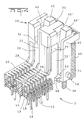
- the electrical connector or socket 2 comprising the preferred embodiment of this invention can be mounted on a substrate 4 in a position to receive a circuit panel 6 so that the circuit panel 6 is positioned transversely relative to the substrate 4.
- This electrical connector or socket 2 is suitable for electrically interconnecting circuits on the substrate 4 to circuits on the circuit panel 6.
- a plurality of integrated circuit components 8 are located on the circuit panels 6 and terminals 10 contained within the electrical connector 2, are adapted to interconnect with traces on a circuit panel 6 leading to the integrated circuit components 8. In this manner the integrated circuit components 8 can be interconnected to traces on the substrate 4.
- Each of the terminals 10 is edge stamped from a spring metal blank. Each terminal has a pair of opposed spring arms 12 and 14 which are outwardly deflectable upon insertion of a circuit panel between the two spring arms.
- a lead 16 extends downwardly from terminals 10 and the leads can be inserted in the holes in a substrate 4 to provide an interconnection between the terminals 10 and traces on the substrate 4.
- An upwardly extending barb 18 engages a central rib in the housing of the electrical connector to retain the terminals in the housing.
- the terminals 10 are positioned within the housing so that they can engage a circuit panel 6 inserted into the housing.
- the electrical connector 2 also includes an insulative housing 20 in which the plurality of terminals 10 are positioned.
- the housing 20 includes a central body 22 and two upright circuit panel support members 24 and 26 at either end thereof.
- the preferred embodiment of the invention depicted herein is suitable for interconnecting two circuit panels 4. Therefore, two upwardly open slots 28, into which circuit panels 6 can be inserted face upwardly along the central body 22.
- the terminals 10 are positioned adjacent the slot 28 and the terminals protrude into the slots so that when a circuit panel 6 is inserted into the slot, the terminals will engage traces on the circuit panel 6.
- the circuit panel support members 24 and 26 extend upwardly above the slot 28 at each end of slot 28.
- the circuit panel support members 24 and 26 are part of a one piece molded housing and these circuit panel support members 24 and 26 extend upwardly at either end of the central body 22.
- Each of the circuit panel support members 24 and 26 include means for holding the circuit panel in a position in which the terminals 10 can engage the circuit panel.
- Each flexible wall 32,32' is located on one side of a recess 30 located in the circuit panel supports 24 and 26 and communicating with the slot 28 so that a circuit panel 6 inserted into the slot 28 will also extend into the recess 30.
- Each flexible wall 30,32' comprises a deflectable member for applying a force to the side of the circuit panel 6 when the circuit panel is positioned in engagement with the terminals 10.
- the flexible wall 32,32' and the gripping means 34,34' are located on one side of recess 30, but it should be understood that flexible walls could be located on opposite sides of recesses 30.
- the gripping means 34,34' in the preferred embodiment of this invention comprises constricting ridges. When a circuit panel 6 is inserted into slot 28 and recess 30, engagement of the circuit panel with the ridges 34,34' will impart deflection to the flexible walls 32,32'.
- flexible walls 32,32' are part of a central support section 36.
- Pockets 40 extending downwardly from the top of the upwardly extending circuit panel support members, are located on opposite sides of the center support section 36. These pockets 40 are generally in alignment with slot 28 and the flexible walls 32,32' are located generally between the pockets 40 and the slots 28.
- Upright guide columns 42,42' extend upwardly from the base of the housing in the pockets 40. The sides of the guide columns 42,42' are spaced from the sides of the pockets 40,40'. Guide columns 42,42' are, however, integral with the end wall 48 of the housing 10.
- Grooves 44 communicating between the pockets 40,40' and the exterior of the support members 24,26 are located adjacent the lower end of support members 24,26. These grooves 44 are straight and the upper end of each groove is enclosed.
- the pockets 40 are configured for receipt of the extraction members 50.
- These circuit panel extraction members 50 are shiftable within the housing 20, relative to the flexible walls 32,32' and the gripping ridges 34,34' which comprise the means for holding the circuit panel 6 in the housing 20.
- the extraction member 50 is shiftable from a first position upwardly to a second position to release a circuit panel 6 from engagement with terminals 10 in the corresponding slot.
- These extraction members 50 are located within the pockets 40 in the circuit panel support member 26, and in the preferred embodiment of this invention two extraction members 50 are located within each a single circuit panel support 26 on one end of the slots 28.
- Each of the extraction members 50 is shiftable in translation, that is in a straight line, relative to the circuit panel support 24,26, and each extraction member 50 is prevented from rotation relative to the circuit panel support 24,26.
- the extraction member 50 comprises two parallel arms 52,54, each extending from a handle 56. These two parallel arms 52 and 54 extend downwardly from spaced apart locations on the handle 56, and in the preferred embodiment of this invention the two arms 52,54 extend from opposite ends of the handle 56.
- Each of the arms 52,54 is L-shaped so that the handle 56 at the upper end of the arms 52,54 will protrude beyond the ends of the circuit panel support member 26 on the insulative housing 20.
- the handles 56 will be easily accessible to permit actuation of the extraction member 50 and movement thereof from the first to the second position so that a circuit panel 6 can be withdrawn from slot 28.
- a crosspiece 62 extends between the two arms at the lower end of each arm 52,54.
- a projection 60 extends inwardly, as seen in Figure 6, from the crosspiece 62 relative to each of the arms 52,54.
- the projection 60 is located below the gripping ridges 34,34' which are used to hold the circuit panel within the slot 28 in engagement with terminals 10.
- the projection 60 also extends below a circuit panel 6, positioned within the slot 28 and protruding into the aligned recess 30.
- Each projection extending laterally of the arms 52,54 below the position of the circuit panel 6, held in engagement with terminals 10, extends inwardly for a sufficient distance to pivot one end of the circuit panel 6 upwardly out of the slot 28.
- the outwardly extending handle 56 extends in the opposite direction from the inwardly direct projection 60 and protrudes beyond the edge of the support member 26. Movement of the handle 56 upwardly will cause the projection to engage the lower edge of a corresponding circuit panel 6 to remove it from a slot 28 and disconnect the circuit panel from terminals 10. It is not necessary that the extraction member be used to completely remove the circuit panel from the housing, because once the extraction apparatus has pivoted the circuit panel, the circuit panel is readily accessible to the operator.
- a protruding member 58 is located on the exterior of at least one arm in the extraction member 50. This protruding member 58 extends from the arm into an interfitting groove 44. Although the protruding member is moveable in the groove 44, the interfitting protruding member 58 and groove 44 cooperate to limit the freedom of movement of the extraction member 50 in at least one direction. In the preferred embodiment of this invention, the interfitting protruding member and the groove act to preclude rotation of the extraction member 50. The interfitting engagement of the protruding member 58 and the groove 44 also serves to prevent removal of the extraction member from the housing, because the protruding member 58 ultimately will engage the closed upper end of the groove 44.
- the extraction members 50 are assembled to the insulative housing by inserting each extraction apparatus 50 into the housing 20 from above.
- the protruding members 58 engage the sides of pockets 40 and the arms 52,54 are sufficiently deformable so that upon engagement of the protruding member 58 with the sides of pocket 40, the arms 52,54 flex inwardly until the protruding member 58 fits within groove 44.
- the extraction member 50 is secured within the corresponding support member 26, but the extraction member 50 is moveable up and down in the support member between a first and second position. Note that one of the extraction members 50 shown in Figure 1 has been moved partially upward relative to the position of the other extraction member. This extraction member has been moved sufficiently upward to cause engagement of the projection 60 with the lower edge of the corresponding circuit panel 6 to pivot the circuit panel partly upwardly relative to the housing.
Landscapes
- Coupling Device And Connection With Printed Circuit (AREA)
- Details Of Connecting Devices For Male And Female Coupling (AREA)
Applications Claiming Priority (2)
| Application Number | Priority Date | Filing Date | Title |
|---|---|---|---|
| US483193 | 1990-02-21 | ||
| US07/483,193 US4990097A (en) | 1990-02-21 | 1990-02-21 | Electrical connector with module extraction apparatus |
Publications (3)
| Publication Number | Publication Date |
|---|---|
| EP0443493A2 true EP0443493A2 (fr) | 1991-08-28 |
| EP0443493A3 EP0443493A3 (en) | 1992-01-22 |
| EP0443493B1 EP0443493B1 (fr) | 1996-09-04 |
Family
ID=23919055
Family Applications (1)
| Application Number | Title | Priority Date | Filing Date |
|---|---|---|---|
| EP91102278A Expired - Lifetime EP0443493B1 (fr) | 1990-02-21 | 1991-02-18 | Connecteur électrique avec appareil d'extraction de module |
Country Status (6)
| Country | Link |
|---|---|
| US (1) | US4990097A (fr) |
| EP (1) | EP0443493B1 (fr) |
| JP (1) | JPH07288153A (fr) |
| KR (1) | KR0125447B1 (fr) |
| CN (1) | CN1030633C (fr) |
| DE (1) | DE69121738T2 (fr) |
Cited By (2)
| Publication number | Priority date | Publication date | Assignee | Title |
|---|---|---|---|---|
| EP0557898B1 (fr) * | 1992-02-24 | 1997-01-29 | Molex Incorporated | Connecteur pour la bordure d'un circuit imprimé |
| WO2006066187A1 (fr) * | 2004-12-14 | 2006-06-22 | Intel Corporation | Systemes et procedes pour connecteur de carte perfectionne |
Families Citing this family (26)
| Publication number | Priority date | Publication date | Assignee | Title |
|---|---|---|---|---|
| US5147211A (en) * | 1991-07-03 | 1992-09-15 | Robinson Nugent, Inc. | Electrical interconnect device with module ejection means |
| US5254017A (en) * | 1991-09-13 | 1993-10-19 | Robinson Nugent, Inc. | Terminal for low profile edge socket |
| US5106315A (en) * | 1991-09-18 | 1992-04-21 | Amp Incorporated | Dual row simm socket ejector |
| US5211568A (en) * | 1992-02-24 | 1993-05-18 | Molex Incorporated | Edge card connector with latch/eject mechanism |
| US5270964A (en) * | 1992-05-19 | 1993-12-14 | Sun Microsystems, Inc. | Single in-line memory module |
| US5302133A (en) * | 1993-05-11 | 1994-04-12 | Robinson Nugent, Inc. | Electrical connector socket with daughtercard ejector |
| US5429523A (en) * | 1993-05-11 | 1995-07-04 | Robinson Nugent, Inc. | Electrical connector socket with daughtercard ejector |
| US5364282A (en) * | 1993-08-16 | 1994-11-15 | Robinson Nugent, Inc. | Electrical connector socket with daughtercard ejector |
| US5389000A (en) * | 1993-11-18 | 1995-02-14 | Molex Incorporated | Edge card connector with improved latch/eject mechanism |
| JP2600949Y2 (ja) * | 1993-12-16 | 1999-11-02 | ヒロセ電機株式会社 | 回路基板挿着用電気コネクタ |
| JP2595705Y2 (ja) * | 1993-12-16 | 1999-06-02 | ヒロセ電機株式会社 | 回路基板挿着用電気コネクタ |
| US5470242A (en) * | 1994-04-20 | 1995-11-28 | Tongrand Limited | Dual readout socket connector |
| US5443394A (en) * | 1994-05-04 | 1995-08-22 | The Whitaker Corporation | Card edge connector having positive lock and extractor |
| US5445531A (en) | 1994-08-23 | 1995-08-29 | The Whitaker Corporation | Card edge connector with shim lock and extractor mechanism |
| US5649831A (en) * | 1995-01-03 | 1997-07-22 | Berg Technology, Inc. | Printed circuit board edge connector including latching and ejectment mechanism |
| US5542854A (en) * | 1995-01-17 | 1996-08-06 | Molex Incorporated | Edge card connector with alignment means |
| USD374540S (en) | 1995-08-25 | 1996-10-15 | Francisco Garza | Snack food |
| JP3355094B2 (ja) | 1996-07-31 | 2002-12-09 | ヒロセ電機株式会社 | 回路基板挿着用電気コネクタ |
| JPH10112360A (ja) | 1996-10-08 | 1998-04-28 | Hirose Electric Co Ltd | 電気コネクタ |
| US6155433A (en) * | 1997-12-01 | 2000-12-05 | Intel Corporation | Dual processor retention module |
| TW401001U (en) * | 1998-12-24 | 2000-08-01 | Hon Hai Prec Ind Co Ltd | Electrical connector |
| CN2842535Y (zh) * | 2005-08-12 | 2006-11-29 | 鸿富锦精密工业(深圳)有限公司 | 板卡固定装置 |
| US20090077293A1 (en) * | 2007-09-07 | 2009-03-19 | International Business Machines Corporation | Dimm Ejection Mechanism |
| US7699644B2 (en) * | 2007-09-28 | 2010-04-20 | Tyco Electronics Corporation | Electrical connector with protective member |
| JP5742800B2 (ja) * | 2012-08-10 | 2015-07-01 | トヨタ自動車株式会社 | 仕切り板および蓄電素子の拘束方法 |
| CN106410452B (zh) * | 2016-11-17 | 2019-06-14 | Oppo广东移动通信有限公司 | 电路板组件及终端 |
Family Cites Families (15)
| Publication number | Priority date | Publication date | Assignee | Title |
|---|---|---|---|---|
| NL132803C (fr) * | 1961-06-12 | |||
| US4241966A (en) * | 1979-04-26 | 1980-12-30 | Thomas & Betts Corporation | Connector with ejector-retainer means |
| US4698024A (en) * | 1982-03-01 | 1987-10-06 | Texas Instrument Incorporated | Rack for input/output modules for a programmable controller |
| US4477138A (en) * | 1982-03-31 | 1984-10-16 | Amp Incorporated | Card biasing device for card edge connectors |
| US4548456A (en) * | 1982-12-21 | 1985-10-22 | Burroughs Corporation | Printed circuit board edge connectors |
| US4531795A (en) * | 1983-03-01 | 1985-07-30 | Aries Electronics, Inc. | Ejector socket for DIP jumpers |
| US4537454A (en) * | 1983-07-25 | 1985-08-27 | Amp Incorporated | Intercard-extraction means |
| US4781612A (en) * | 1983-12-14 | 1988-11-01 | Amp Incorporated | Socket for single in-line memory module |
| US4557548A (en) * | 1983-12-14 | 1985-12-10 | Amp Incorporated | Edge connector for chip carrier |
| US4558912A (en) * | 1983-12-14 | 1985-12-17 | Amp Incorporated | Edge connector for chip carrier |
| JPS6369375U (fr) * | 1986-10-27 | 1988-05-10 | ||
| US4722700A (en) * | 1987-01-23 | 1988-02-02 | Amp Incorporated | Low insertion force terminal for use with circuit panel |
| US4725250A (en) * | 1987-01-27 | 1988-02-16 | Amp Incorporated | High density circuit panel socket |
| JPH01175180A (ja) * | 1987-12-28 | 1989-07-11 | Yamaichi Electric Mfg Co Ltd | 配線基板用コネクタ |
| JPH0541509Y2 (fr) * | 1988-03-03 | 1993-10-20 |
-
1990
- 1990-02-21 US US07/483,193 patent/US4990097A/en not_active Expired - Lifetime
-
1991
- 1991-02-18 EP EP91102278A patent/EP0443493B1/fr not_active Expired - Lifetime
- 1991-02-18 DE DE69121738T patent/DE69121738T2/de not_active Expired - Fee Related
- 1991-02-20 KR KR1019910002697A patent/KR0125447B1/ko not_active Expired - Fee Related
- 1991-02-20 CN CN91101105.6A patent/CN1030633C/zh not_active Expired - Fee Related
- 1991-02-21 JP JP3047316A patent/JPH07288153A/ja active Pending
Cited By (2)
| Publication number | Priority date | Publication date | Assignee | Title |
|---|---|---|---|---|
| EP0557898B1 (fr) * | 1992-02-24 | 1997-01-29 | Molex Incorporated | Connecteur pour la bordure d'un circuit imprimé |
| WO2006066187A1 (fr) * | 2004-12-14 | 2006-06-22 | Intel Corporation | Systemes et procedes pour connecteur de carte perfectionne |
Also Published As
| Publication number | Publication date |
|---|---|
| CN1054336A (zh) | 1991-09-04 |
| EP0443493A3 (en) | 1992-01-22 |
| JPH07288153A (ja) | 1995-10-31 |
| CN1030633C (zh) | 1996-01-03 |
| DE69121738D1 (de) | 1996-10-10 |
| KR0125447B1 (ko) | 1997-12-22 |
| DE69121738T2 (de) | 1997-01-02 |
| EP0443493B1 (fr) | 1996-09-04 |
| US4990097A (en) | 1991-02-05 |
Similar Documents
| Publication | Publication Date | Title |
|---|---|---|
| US4990097A (en) | Electrical connector with module extraction apparatus | |
| US4973270A (en) | Circuit panel socket with cloverleaf contact | |
| JP2649988B2 (ja) | 基板用電気コネクタ | |
| KR950012748B1 (ko) | 전기 접속기 | |
| EP0416322B1 (fr) | Borne de contact dans un support pour platine de circuits | |
| US5676555A (en) | Card edge connector having means for applying inward transverse force on printed wiring boards | |
| KR0123573Y1 (ko) | 에찌 콘넥터 | |
| KR100347242B1 (ko) | 일체형지지구조를갖춘전기커넥터 | |
| US4018494A (en) | Interconnection for electrically connecting two vertically stacked electronic packages | |
| EP0232103B1 (fr) | Agencement de broche et alvéole de prise de courant électrique pour connecteurs à fiches et douilles | |
| US5046972A (en) | Low insertion force connector and contact | |
| EP0499378A2 (fr) | Socle simm de profil bas actionné par came | |
| US5254017A (en) | Terminal for low profile edge socket | |
| US4722700A (en) | Low insertion force terminal for use with circuit panel | |
| US4354718A (en) | Dual-in-line package carrier and socket assembly | |
| US5131872A (en) | Contact spring socket | |
| EP0122486B1 (fr) | Connecteurs électriques avec des broches quasi-terminales | |
| US4725250A (en) | High density circuit panel socket | |
| US5366390A (en) | Low profile cam-in socket having terminals engaging a rib | |
| EP0400378A2 (fr) | Socle de panneau de circuit imprimé à contact en forme de trèfle | |
| US5865649A (en) | Card edge connector having means for preventing overstress of contact elements | |
| EP0299989B1 (fr) | Prise pour plaquette de circuit a haute densite | |
| WO1996002960A1 (fr) | Force d'introduction nulle pour support de puce en plastique | |
| EP1107371A1 (fr) | Connecteur | |
| US4968259A (en) | High density chip carrier socket |
Legal Events
| Date | Code | Title | Description |
|---|---|---|---|
| PUAI | Public reference made under article 153(3) epc to a published international application that has entered the european phase |
Free format text: ORIGINAL CODE: 0009012 |
|
| AK | Designated contracting states |
Kind code of ref document: A2 Designated state(s): DE FR GB IT NL |
|
| PUAL | Search report despatched |
Free format text: ORIGINAL CODE: 0009013 |
|
| AK | Designated contracting states |
Kind code of ref document: A3 Designated state(s): DE FR GB IT NL |
|
| 17P | Request for examination filed |
Effective date: 19920610 |
|
| RAP1 | Party data changed (applicant data changed or rights of an application transferred) |
Owner name: THE WHITAKER CORPORATION |
|
| 17Q | First examination report despatched |
Effective date: 19940601 |
|
| GRAH | Despatch of communication of intention to grant a patent |
Free format text: ORIGINAL CODE: EPIDOS IGRA |
|
| GRAH | Despatch of communication of intention to grant a patent |
Free format text: ORIGINAL CODE: EPIDOS IGRA |
|
| GRAA | (expected) grant |
Free format text: ORIGINAL CODE: 0009210 |
|
| AK | Designated contracting states |
Kind code of ref document: B1 Designated state(s): DE FR GB IT NL |
|
| ITF | It: translation for a ep patent filed | ||
| REF | Corresponds to: |
Ref document number: 69121738 Country of ref document: DE Date of ref document: 19961010 |
|
| ET | Fr: translation filed |
Free format text: CORRECTIONS |
|
| PLBE | No opposition filed within time limit |
Free format text: ORIGINAL CODE: 0009261 |
|
| STAA | Information on the status of an ep patent application or granted ep patent |
Free format text: STATUS: NO OPPOSITION FILED WITHIN TIME LIMIT |
|
| 26N | No opposition filed | ||
| PGFP | Annual fee paid to national office [announced via postgrant information from national office to epo] |
Ref country code: NL Payment date: 19981222 Year of fee payment: 9 |
|
| PGFP | Annual fee paid to national office [announced via postgrant information from national office to epo] |
Ref country code: DE Payment date: 19990226 Year of fee payment: 9 |
|
| PGFP | Annual fee paid to national office [announced via postgrant information from national office to epo] |
Ref country code: FR Payment date: 20000207 Year of fee payment: 10 |
|
| PG25 | Lapsed in a contracting state [announced via postgrant information from national office to epo] |
Ref country code: NL Free format text: LAPSE BECAUSE OF NON-PAYMENT OF DUE FEES Effective date: 20000901 |
|
| NLV4 | Nl: lapsed or anulled due to non-payment of the annual fee |
Effective date: 20000901 |
|
| PG25 | Lapsed in a contracting state [announced via postgrant information from national office to epo] |
Ref country code: DE Free format text: LAPSE BECAUSE OF NON-PAYMENT OF DUE FEES Effective date: 20001201 |
|
| PG25 | Lapsed in a contracting state [announced via postgrant information from national office to epo] |
Ref country code: FR Free format text: LAPSE BECAUSE OF NON-PAYMENT OF DUE FEES Effective date: 20011031 |
|
| REG | Reference to a national code |
Ref country code: FR Ref legal event code: ST |
|
| REG | Reference to a national code |
Ref country code: GB Ref legal event code: IF02 |
|
| PG25 | Lapsed in a contracting state [announced via postgrant information from national office to epo] |
Ref country code: IT Free format text: LAPSE BECAUSE OF NON-PAYMENT OF DUE FEES Effective date: 20050218 |
|
| PGFP | Annual fee paid to national office [announced via postgrant information from national office to epo] |
Ref country code: GB Payment date: 20100224 Year of fee payment: 20 |
|
| REG | Reference to a national code |
Ref country code: GB Ref legal event code: PE20 Expiry date: 20110217 |
|
| PG25 | Lapsed in a contracting state [announced via postgrant information from national office to epo] |
Ref country code: GB Free format text: LAPSE BECAUSE OF EXPIRATION OF PROTECTION Effective date: 20110217 |