EP0442571B1 - Bildwiedergaberöhre mit Elektronenstrahlerzeugungssystem mit Fokussierungslinse vom Spiraltyp - Google Patents
Bildwiedergaberöhre mit Elektronenstrahlerzeugungssystem mit Fokussierungslinse vom Spiraltyp Download PDFInfo
- Publication number
- EP0442571B1 EP0442571B1 EP19910200279 EP91200279A EP0442571B1 EP 0442571 B1 EP0442571 B1 EP 0442571B1 EP 19910200279 EP19910200279 EP 19910200279 EP 91200279 A EP91200279 A EP 91200279A EP 0442571 B1 EP0442571 B1 EP 0442571B1
- Authority
- EP
- European Patent Office
- Prior art keywords
- voltage
- resistance
- focusing
- low
- display device
- Prior art date
- Legal status (The legal status is an assumption and is not a legal conclusion. Google has not performed a legal analysis and makes no representation as to the accuracy of the status listed.)
- Expired - Lifetime
Links
- 238000012937 correction Methods 0.000 claims description 29
- 238000010894 electron beam technology Methods 0.000 claims description 21
- 229910052751 metal Inorganic materials 0.000 claims description 17
- 239000002184 metal Substances 0.000 claims description 17
- 230000003068 static effect Effects 0.000 claims description 11
- 230000000694 effects Effects 0.000 claims description 10
- 239000000463 material Substances 0.000 claims description 10
- 230000003247 decreasing effect Effects 0.000 claims description 4
- 239000004020 conductor Substances 0.000 claims description 3
- 238000010276 construction Methods 0.000 description 11
- 239000011521 glass Substances 0.000 description 9
- 238000010586 diagram Methods 0.000 description 4
- 238000000034 method Methods 0.000 description 3
- 230000004075 alteration Effects 0.000 description 2
- 239000011248 coating agent Substances 0.000 description 2
- 238000000576 coating method Methods 0.000 description 2
- 238000000151 deposition Methods 0.000 description 2
- 230000008021 deposition Effects 0.000 description 2
- 229910044991 metal oxide Inorganic materials 0.000 description 2
- 150000004706 metal oxides Chemical class 0.000 description 2
- 238000010422 painting Methods 0.000 description 2
- 238000004544 sputter deposition Methods 0.000 description 2
- VYZAMTAEIAYCRO-UHFFFAOYSA-N Chromium Chemical compound [Cr] VYZAMTAEIAYCRO-UHFFFAOYSA-N 0.000 description 1
- 229910002467 CrFe Inorganic materials 0.000 description 1
- OAICVXFJPJFONN-UHFFFAOYSA-N Phosphorus Chemical compound [P] OAICVXFJPJFONN-UHFFFAOYSA-N 0.000 description 1
- 239000004411 aluminium Substances 0.000 description 1
- 229910052782 aluminium Inorganic materials 0.000 description 1
- XAGFODPZIPBFFR-UHFFFAOYSA-N aluminium Chemical compound [Al] XAGFODPZIPBFFR-UHFFFAOYSA-N 0.000 description 1
- ILRRQNADMUWWFW-UHFFFAOYSA-K aluminium phosphate Chemical compound O1[Al]2OP1(=O)O2 ILRRQNADMUWWFW-UHFFFAOYSA-K 0.000 description 1
- 229940001007 aluminium phosphate Drugs 0.000 description 1
- 229910000147 aluminium phosphate Inorganic materials 0.000 description 1
- 239000000919 ceramic Substances 0.000 description 1
- 229910010293 ceramic material Inorganic materials 0.000 description 1
- 229910052804 chromium Inorganic materials 0.000 description 1
- 239000011651 chromium Substances 0.000 description 1
- 230000008878 coupling Effects 0.000 description 1
- 238000010168 coupling process Methods 0.000 description 1
- 238000005859 coupling reaction Methods 0.000 description 1
- 238000005520 cutting process Methods 0.000 description 1
- 210000003298 dental enamel Anatomy 0.000 description 1
- 238000005137 deposition process Methods 0.000 description 1
- 238000006073 displacement reaction Methods 0.000 description 1
- 230000005686 electrostatic field Effects 0.000 description 1
- 238000005530 etching Methods 0.000 description 1
- 239000011888 foil Substances 0.000 description 1
- 239000002241 glass-ceramic Substances 0.000 description 1
- 238000010438 heat treatment Methods 0.000 description 1
- 229910052738 indium Inorganic materials 0.000 description 1
- APFVFJFRJDLVQX-UHFFFAOYSA-N indium atom Chemical compound [In] APFVFJFRJDLVQX-UHFFFAOYSA-N 0.000 description 1
- 238000009413 insulation Methods 0.000 description 1
- 210000001503 joint Anatomy 0.000 description 1
- 238000004519 manufacturing process Methods 0.000 description 1
- 230000005405 multipole Effects 0.000 description 1
- 230000003287 optical effect Effects 0.000 description 1
- 230000003647 oxidation Effects 0.000 description 1
- 238000007254 oxidation reaction Methods 0.000 description 1
- 230000001590 oxidative effect Effects 0.000 description 1
- 239000003973 paint Substances 0.000 description 1
- 239000002245 particle Substances 0.000 description 1
- 239000008188 pellet Substances 0.000 description 1
- 239000005365 phosphate glass Substances 0.000 description 1
- 239000011253 protective coating Substances 0.000 description 1
- 229910001925 ruthenium oxide Inorganic materials 0.000 description 1
- WOCIAKWEIIZHES-UHFFFAOYSA-N ruthenium(iv) oxide Chemical compound O=[Ru]=O WOCIAKWEIIZHES-UHFFFAOYSA-N 0.000 description 1
- 238000005488 sandblasting Methods 0.000 description 1
- 238000007493 shaping process Methods 0.000 description 1
- 238000005507 spraying Methods 0.000 description 1
- 229920002994 synthetic fiber Polymers 0.000 description 1
- 238000003466 welding Methods 0.000 description 1
Images
Classifications
-
- H—ELECTRICITY
- H01—ELECTRIC ELEMENTS
- H01J—ELECTRIC DISCHARGE TUBES OR DISCHARGE LAMPS
- H01J29/00—Details of cathode-ray tubes or of electron-beam tubes of the types covered by group H01J31/00
- H01J29/46—Arrangements of electrodes and associated parts for generating or controlling the ray or beam, e.g. electron-optical arrangement
- H01J29/58—Arrangements for focusing or reflecting ray or beam
- H01J29/62—Electrostatic lenses
- H01J29/622—Electrostatic lenses producing fields exhibiting symmetry of revolution
-
- H—ELECTRICITY
- H01—ELECTRIC ELEMENTS
- H01J—ELECTRIC DISCHARGE TUBES OR DISCHARGE LAMPS
- H01J2229/00—Details of cathode ray tubes or electron beam tubes
- H01J2229/48—Electron guns
- H01J2229/4824—Constructional arrangements of electrodes
- H01J2229/4827—Electrodes formed on surface of common cylindrical support
Definitions
- the invention relates to a picture display device comprising a display tube having a display screen and an electron gun arranged on an electron-optical axis for producing an electron beam directed along said axis toward said screen, said electron gun comprising, arranged along said axis, an electron beam producing part for producing the electron beam and a tubular structure, through which the electron beam passes, for effecting focusing the electron beam to form a spot for deflection across the screen, said tubular structure having an outer surface and an inner surface on one of which a resistance structure of a material having a high electrical resistance is provided
- the resistance structure has at least one contact for supplying a static focusing voltage and at least one contact for supplying an anode voltage.
- It is an object of the invention to provide a picture display device comprising a display tube with an electrostatic lens, such as a focusing lens, of the helical resistance type, which is particularly suitable for using dynamic correction signals.
- the resistance structure comprises a first and a second electrical contact which are axially spaced apart and which are connected to a first voltage-providing means for applying an anode voltage V a , the resistance structure further being in electrical contact with a low-ohmic electrode means intermediate the first and second electrical contact, the low-ohmic electrode means connected to second voltage-providing means for applying a static focusing voltage V f (stat), whereby, in operation, an electron-optic main-focusing lens of the unipotential or quadri-potential type or other, non-bipotential, multipotential type is formed, and a dynamic correction voltage V f (dyn), whereby, in operation, in the tubular structure a localized dynamic electron-optical element is formed in the region of the low-ohmic electrode means.
- V f static focusing voltage
- V f dynamic correction voltage
- the invention is based, inter alia, on the recognition that the high resistance of the (helical) lens structure leads to a long intrinsic RC time of the resistance layer, even at those locations where the layer does not form a helical structure but is homogeneous. In other words, the focusing signal does not propagate or hardly propagates in the resistance structure.
- the electrical connection of the high-ohmic resistance structure to the above-described low-ohmic electrode means provides a region having an RC time which is decreased to such an extent that the dynamic correction signal can spread sufficiently far across the main focusing lens in the central part of the focusing lens.
- the intermediate electrode means may consist of, for example a coaxial metal ring, one or more transversal metal plates having a beam-passing aperture or of a thin conducting layer provided on the inner wall of the tubular structure and/or on the inner surface of the resistance structure. Vapour deposition, sputtering or painting are examples of suitable techniques for providing the thin conducting layer. It appears that dynamic correction signals (such as, for example dynamic focusing signals) having frequencies up to the MHz range now provide the desired effect.
- a construction enabling the low-ohmic intermediate electrode to be provided in a simple manner is characterized in that the tubular structure comprises at least two aligned sub-tubes each having resistance structures which jointly constitute a main focusing lens and in that the low-ohmic electrode means consists of at least one metal plate having a beam-passing aperture, which plate is arranged transversely between the facing ends of the sub-tubes.
- An embodiment of this construction is characterized in that the beam-producing part comprises a correction means for correcting possible alignment errors of the sub-tubes.
- a construction with which alignment errors are obviated is characterized in that the tubular structure comprises a single tube having a resistance structure provided on its inner surface, which structure when energized constitutes a main-focusing lens, in that an annular structure of electrically conducting material making electrical contact with the resistance structure is arranged within said tube, which annular structure constitutes the low-ohmic electrode means, and in that the annular structure is connected to an electric contact via an aperture in the wall of the tube.
- the low-ohmic intermediate electrode is constructed to exercise a rotationally symmetrical effect on the electron beam.
- the low-ohmic intermediate electrode should be constructed to exercise a non-rotationally symmetrical effect.
- a display tube comprising an electron gun having a beam-shaping part and a focusing lens structure of the so-called bipotential type is described.
- the focusing structure comprises an elongate hollow structure with a high-ohmic resistive layer provided on the inner and/or outer surface. A voltage is applied across the high-ohmic resistive layer.
- the focusing structure comprises means for forming a non-rotationally symmetrical lens element in the area of the focusing structure. If astigmatic corrections are desired these corrections are provided in between a prefocusing and a main-focusing lens of the focusing lens structure.
- FR-A 1 407 985 an improved electrostatic electron optical system suitable for use in picture signal generating tubes is described in which a collimating electrostatic field is formed in a lens comprising a non-linear spiral electrode which is particularly shaped and arranged to minimize spherical aberration of the electron beam.
- the spiral electrode is replaced by two coaxial linearly spaced spiral electrodes separated by a cylindrical band, which band is connected to a separate source of lower potential. By adjusting the potential of the cylindrical band, the degree of collimation of the latter structure is easily controlled.
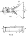
- the device shown in Fig. 1 comprises a cathode ray tube consisting of, inter alia, a glass envelope 1 which is composed of a display window 2, a conical portion 3 and a neck 4.
- This neck accommodates electrode structures 8 and 9 which together with a cathode constitute the beam-producing part 43 of an electron gun.
- the electron-optical axis 6 of the electron gun is also the axis of the envelope.
- An electron beam 12 is successively formed and accelerated by the cathode 7 and the electrode structures 8, 9.
- the reference numeral 10 denotes a tubular structure whose inner surface carries a (particularly helical) structure 11 of a material having a very high electrical resistance which forms a focusing lens focusing the beam on a display screen 14 on the inner side of the display window 2.
- the resistance structure 11 is electrically connected to a low-ohmic metal input electrode 13a and a low-ohmic metal output electrode 13b.
- suitable voltages to be applied to the electrodes are, for example:
- a low-ohmic electrode is required within the scope of the invention.
- This electrode may be constructed in different manners. Examples will be given with reference to Figs. 5, 6, 7 and 8.
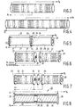
- the type in question comprises a tubular (glass) envelope 15.
- the inner side of the envelope 15 whose ends are provided with transversal metal electrode plates 17a, 17b having central coaxial apertures 18a, 18b carries a high-ohmic resistance layer 16 in which a helical structure is formed which constitutes a focusing lens 17 when a suitable electric voltage is applied.
- the patterns of parallel oblique lines diagrammatically represent the locations where the resistance layer 16 has been omitted. The parts of the helical structure are thus always present between two of these lines.
- the high-ohmic resistance layer 16 may consist of, for example glass enamel having a small amount (for example several % by weight) of metal oxide (particularly ruthenium oxide) particles.
- the layer 16 may have a thickness of between 1 and 10 ⁇ m, for example 3 ⁇ m.
- the resistance per square of such a layer depends on the concentration of metal oxide and the heat treatment to which the layer is subjected. In practice resistances per square varying between 10 4 and 10 8 ⁇ have been realised. A desired resistance per square can be realised by adjusting the relevant parameters. A resistance per square of the order of 10 6 ⁇ is very suitable for the relevant application.
- the total resistance of the helical structure formed in the layer 16 (which structure may comprise a continuous helix as well as a number of separate helixes connected by segments without a helical structure - 6 in the example of Fig. 2) may be of the order of 10 G ⁇ , which means that a current of several mA will flow across the ends at a voltage difference of 30 kV.
- the (oblique) line patterns indicate the locations of the resistance layer where the material has been removed from the resistance layer by means of, for example, a rotating cutting tool.
- the electron gun of Fig. 1 has a beam-producing part 43 preceding the focusing lens 17, which part generally comprises a cathode 7, a grid electrode 8 and an anode 9.
- the components of the beam-producing part 43 are separately mounted in the display tube, for example, by means of axial glass- ceramic mounting rods. Alternatively, they may be mounted within the tubular envelope 10 of the focusing lens.
- the power of the electron lens for focusing the electron beam is adjusted as a function of the deflection to which the electron beam is subjected at that instant. This provides the possibility of causing the main picture plane which is then prevalent to intersect the display screen at the location where the electron beam impinges upon the display screen.
- This correction mode requires an extra circuit in the control device for generating the correct dynamic focusing voltages on the electrodes of the focusing lens.
- the material of the helical resistance structure has such a high electrical resistance (for example 10 G ⁇ ), the RC time is long (for example 10 msec). As a result, the effect of a dynamic focusing voltage applied to electrode 17a will hardly reach the helical resistance structure.
- the invention provides a solution in this respect. The principle of this solution will be elucidated with reference to Figs. 3 and 4 showing two designs of focusing lenses which are suitable for use in an electron gun for a picture display device according to the invention.
- Fig. 3 shows diagrammatically a helical focusing lens in which an anode voltage V a is applied to the ends and a focusing voltage V f is applied to the central part (so-called unipotential lens).
- V a anode voltage
- V f focusing voltage
- a characteristic feature of a unipotential lens design is that, in contrast to a bipotential lens design, the voltages across the object-sided lens portion and the image-sided lens portion are equal.
- the resistance structures of these two portions may be symmetrical. Each structure has, for example 5 helical segments.
- Fig. 4 shows diagrammatically a helical focusing lens in which an anode voltage V a is applied to one end and to a first part located between the ends, and a focusing voltage V f is applied to the other end and to a second part located between the ends (so-called quadripotential lens).
- Such a lens may have an object-sided potential at the focusing voltage, followed by a trajectory where the potential increases to the anode voltage and then the potential may decrease to the focusing voltage and increase again to the anode voltage on the last trajectory.
- the voltages can be applied, for example by making an aperture in the wall of the glass tube at each desired location, which glass tube carries the resistance structure on its inner surface, and by providing an electric contact in this aperture (for example an indium pellet) which makes contact with the resistance layer.
- an electric contact in this aperture for example an indium pellet
- a metal flange making electrical contact with the resistance layer can be provided at the ends of the glass tube.
- the electrode for applying a dynamic correction signal should always be a low-ohmic intermediate electrode electrically connected to the resistance layer.
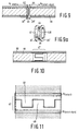
- FIG. 5 An embodiment of the lens design of Fig. 3 is shown in Fig. 5.
- the resistance lens construction shown in this Figure comprises a sub-tube 21 and a sub-tube 22.
- Metal flanges (for example flanges of CrFe) 23, 24 each having a coaxial aperture are sealed to the ends of sub-tube 21 and metal flanges 25, 26 each having a coaxial aperture are sealed to the ends of the sub-tube 22.
- the flanges 23, 26 serve for applying the anode voltage V a .
- high-ohmic resistance layers 27, 28 having a helical structure are arranged in the sub-tubes 21, 22.
- the flanges 24, 25, each of which has a beam-passing aperture are welded together and jointly constitute a low-ohmic intermediate electrode which serves for applying the (static + dynamic) focusing voltage V f .
- Fig. 6 shows a substantially identical structure. However, in this case the facing flanges 24, 25 are not welded together, but arranged in a mutually electrically insulated manner (for example, by mounting on glass or ceramic rods which are not shown). This provides the possibility of applying a static plus a dynamic focusing voltage V f (stat + dyn) to, for example flange 25 and a static focusing voltage V f (stat) to flange 24.
- the metal flanges 24, 25 having coaxial central apertures 29, 30 function as low-ohmic electrodes.
- the apertures 29, 30 may have a rotationally symmetrical shape, as in Fig. 5.
- the apertures 29, 30 have a non-rotationally symmetrical shape, for example a square or elongate (oval or rectangular) shape, as in Fig. 6, an electric 4-pole field forming an astigmatic lens is formed in between them upon energization.
- the applied dynamic focusing voltage has a diverging effect on an electron beam passing through the focusing lens, both in the horizontal and in the vertical direction. This diverging effect can be compensated in the horizontal direction and increased in the vertical direction by the astigmatic lens which is formed between the flanges 24, 25 when the dynamic and static focusing voltages are applied. This renders an independent horizontal and vertical focusing possible, which is particularly important in color display tubes. (Here, dynamic astigmatic focusing is concerned).
- Fig. 7 shows a structure which is substantially identical to the structure of the focusing lens of Fig. 6. In this case, however, an extra transversal electrode 31 is arranged between the flanges 24 and 25. The required static and dynamic focusing voltages can now be separately applied to the electrodes 24, 25 and 31.
- Fig. 9 shows a part of a focusing lens construction with a low-ohmic electrode means comprising two metal flanges 24' and 25' each having a beam-passing aperture and engaging projections 42, 430, 44 and 45 whereby, upon energization, a 4-pole field is generated between the flanges.
- a 4-pole field is generated between the flanges.
- the focusing lens always comprises at least two sub-tubes having a resistance structure. This could give rise to misalignment of the sub-tubes. Possibly occurring misalignments can be corrected by a correction means particularly arranged in front of the focusing lens.
- the desired correction is realised, for example, by providing a ring 55 of permanently magnetizable material in the last electrode of the beam-producing part of the electron gun (electrode 9 in Fig. 1) and by magnetizing this ring from the exterior after the electron gun has been mounted in the display tube. It appears from Figs.
- the metal flanges 24, 25 (and 31) are comparatively close to the through-connection wire 32 applying the anode (high) voltage to flange 23. Since the flanges 24, 25 (and 31) convey the (lower) focusing voltage, this may give rise to unwanted field emission ("spraying") of the flanges 24, 25 (and 31) to the through-connection wire 32, particularly when the flanges are rough (or have projections). To prevent this, it should be ensured that the components conveying different voltages do not "see" one another, for example, by insulating the connection wire by oxidizing the material of which it is made or by coating it with an insulating layer.
- an electrically insulating protective coating is preferably provided on the components conveying the lowest voltage (i.e. the flanges 24, 25 (and 31)).
- a thin layer of ceramic material or of glass is suitable for insulation.
- aluminium phosphate glass is a good choice.
- This may be provided in a thin layer and has a high viscosity already at a relatively low temperature. Consequently, a great degree of freedom with respect to the coefficients of expansion of the metal to be coated and the glass is admissible.
- this layer will easily follow possible irregularities of the surface on which it is provided and thus coat this surface satisfactorily.
- An alternative example is to manufacture the flanges 24, 25 (and 31) from a chromium-containing material and to subject it to an oxidation treatment.
- the focusing lens 33 comprises one single tube 34 (having a length of, for example 70 mm) in this case.
- the inner surface of tube 34 is provided, for example in the manner described hereinbefore with a high-ohmic resistance layer 35 having a helical pattern and its ends may be provided with flanges 36, 37 which are electrically connected thereto and are intended to apply an anode voltage V a .
- the tube 34 accommodates a coaxial metal ring 38 (for example of CrNi) which is in (clamping) engagement and in electrical contact with a part of the resistance layer 35 in which no helical pattern has been provided.
- Focus lead 40 is welded (for example by means of laser welding) to the clamping ring 38 functioning as a focusing electrode via an aperture 39 (of, for example 1.5 x 3 mm) in the wall of the tube 34, which aperture is made (for example by means of sandblasting) preferably after the resistance layer 35 is provided.
- the wall of the tube 34 shields the focusing electrode 38 from anode through-connection wire 41, thus preventing the above-mentioned field emission problem.
- the width of the focusing electrode (clamping ring 38 in this case) determines to a considerable extent the region where dynamic focusing takes place. Also the width of the uninterrupted part of the resistance layer 35 located between the helical portions plays a role if this width deviates from the width of the focusing electrode. Static focusing takes place throughout the length of the helical pattern.
- the focus lead 40 does not "see” the high-voltage through-connection wire 41.
- coaxial focusing ring 38 is rotationally symmetrical so as to render the use of dynamic focusing possible.
- rotationally symmetrical rings are not only understood to mean (closed) rings whose circumference exactly follows a circular path, but also (open) substantially circular rings with two ends which slightly overlap or with two ends which are located opposite each other in one plane, either with the inclusion of a small gap or by means of a butt joint.
- a layer or a tape of electrically conducting (low-ohmic) material can be used as a focusing electrode.
- Such a layer can be provided on the inner wall of the tube 34 before the high-ohmic resistance structure 35 is provided.
- An alternative method is to provide the high-ohmic resistance structure 35 and to coat it with a layer of electrically conducting material, for example a layer of electrically conductive paint sold under the name of "Leitsilber".
- the invention can be used for dynamic astigmatic focusing, for which purpose an electric 4-pole field is generated in the focusing lens range.
- it may also be used for generating other dynamic multipole fields in the focusing lens range, for example, a dynamic dipole field (for beam displacement).
- the inventive principle of ohmically coupling in a dynamic signal into a resistance lens may be used advantageously in a projection TV tube, but the principle may also be used in color display tubes.
- Another possibility is its use in oscilloscope tubes in which the high-frequency deflection could be effected, for example by means of a signal which is ohmically coupled in, similarly as the dynamic focusing signal.
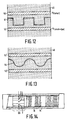
- D ynamic a stigmatic f ocusing may be carried out in manners differing from those described hereinbefore, for example, in the manner shown in Fig. 10.
- the resistance layer 46 of the focusing lens is interrupted over an intermediate area 47 of several millimetres.
- the inner wall of the tubular structure 50 carries two metal electrodes 48, 49 which have engaging projections of several millimetres' length.
- Each electrode 48, 49 slightly overlaps the resistance layer 46 so as to establish electrical contact therewith.
- the electrodes may be made of, for example, a layer of a low-ohmic material provided by way of an electroless or a vapour-deposition process, in which the finger structure is provided by means of etching or by a laser.
- the support may be a synthetic material foil. Electrodes of the type 24', 25' shown in Fig. 9 are alternatively possible. Fig. 11 shows the area 47 and its direct surroundings in greater detail. A voltage V f (stat) is applied to the electrode 48 and a voltage V f (stat + dyn) is applied to the electrode 49.
- Fig. 12 shows a simpler solution.
- the resistance layer 46 in which the helical pattern is formed, is not interrupted over a given (intermediate) area (as in the constructions shown in Figs. 5, 6, 7, 9, 10 and 11), but it continues as in the construction shown in Fig. 8.
- a finger structure is formed by means of a scratch 51 in the resistance layer 46. (There may be a plurality of parallel scratches so as to reduce the voltage drop per scratch.)
- An annular structure in the form of two tape-shaped metal electrodes 52, 53 is provided on both sides at a short distance (several mm) from this scratch. These electrodes are energized in the same way as the electrodes shown in Fig. 11.
- DAF is possible at the line frequency as well as at the field frequency, when the latter two solutions are employed. Another advantage is that DAF electrodes having a finger structure are very effective.
- a further refinement is to replace the rectangular finger (or square-wave) structure by a more gradual profile such as a sin2 ⁇ function.
- Such a scratch 54 is easier to provide and will result in fewer lens errors.
- use is made of tape-shaped electrodes 52' and 53' to which respective voltages V f (stat) and V f (stat + dyn) are applied.
- the invention is generally based on the recognition that the high resistance of the resistance structure leads to a long intrinsic RC time, even at those locations where the layer does not form a helical structure, so that a H.F. correction signal, such as a dynamic focusing signal, does not enter or hardly enters into the resistance structure. This also holds in the case where a portion of the resistance structure outside the focusing lens portion constitutes a correction element.
- This may be a correction element of a type described hereinbefore, or a cylindrical element 60 which has a plurality of circumferentially arranged parts (for example, 2, 4 or 8), each of which is adapted to be connected to voltage-providing means for applying a correction voltage and each of which is in contact with a low-ohmic electrode means for decreasing its resistance (see Fig. 14).
- Each low-ohmic electrode means should at least be in contact with its own correction element part in the area of the voltage contact.
- the correction element parts can be electrically connected to the resistance structure portion constituting a focusing lens.
- a further aspect of the invention thus is that contacting each individual portion of the high-ohmic correction element with a low-ohmic electrode means provides a region having an RC time which is decreased to such an extent that the dynamic correction signal can spread fast enough across the correction element to be effective.
- the low-ohmic electrode means may consist of, for example, a thin conducting layer provided on the inner wall of the tubular structure. Vapour deposition, sputtering or painting are examples of suitable techniques for providing the thin conducting layer. It appears that dynamic correction signals (such as, for example dynamic focusing signals) having frequencies up to the MHz range now provide the desired effect.
Landscapes
- Vessels, Lead-In Wires, Accessory Apparatuses For Cathode-Ray Tubes (AREA)
- Cathode-Ray Tubes And Fluorescent Screens For Display (AREA)
Claims (8)
- Bildwiedergaberöhre mit einer Bildröhre mit einem Bildschirm (14) und einem demselben gegenüber liegenden Elektronenstrahlerzeugungssystem auf einer elektronenoptischen Achse zum Erzeugen eines Elektronenstrahls, der über die genannte Achse auf den genannten Schirm (14) gerichtet ist, wobei dieses Elektronenstrahlerzeugungssystem, längs der genannten Achse vorgesehen, einen Elektronenstrahlerzeugungsteil (43) zum Erzeugen des Elektronenstrahls und eine röhrenförmige Struktur (10) aufweist, durch die der Elektronenstrahl hindurchgeht, zum Herbeiführen einer Fokussierung des Elektronenstrahls zum Bilden eines Punktes zur Ablenkung über den Schirm (14), wobei die genannte röhrenförmige Struktur (10) eine Außenoberfläche und eine Innenoberfläche aufweist, wobei auf einer dieser Oberflächen eine Widerstandsstruktur (11) aus einem Material mit einem hohen elektrischen Widerstand vorgesehen ist, wobei die Widerstandsstruktur (11) einen ersten und einen zweiten elektrischen Kontakt (23, 26, 37, 36) aufweist, die axial in einem Abstand voneinander liegen und mit einem ersten Speisemittel verbunden sind zum Zuführen einer Anodenspannung Va, wobei die Widerstandsstruktur (11) weiterhin mit einem niederohmigen Elektrodenmittel (24, 31, 25) zwischen dem ersten und dem zweiten elektrischen Kontakt (23, 26, 37, 36) elektrisch kontaktiert ist, wobei das niederohmige Elektrodenmittel (24, 31, 25) mit einem zweiten Speisemittel kontaktiert ist zum Liefern einer statischen Fokussierungsspannung Vf(stat), wodurch im Betrieb eine elektronenoptische Hauptfokussierungslinse vom Einpotential- oder vom Vierpotentialtyp oder aber von einem anderen nicht-bipotentialen, Multipotentialtyp gebildet wird, sowie einer dynamischen Korrekturspannung Vf(dyn), wodurch im Betrieb in der Röhrenstruktur (10) im Bereich des niederohmigen Elektrodenmittels (24, 31, 25) ein örtlich dynamisches elektronenoptisches Element gebildet wird.
- Wiedergabeanordnung nach Anspruch 1, dadurch gekennzeichnet, daß das niederohmige Elektrodenmittel (24, 31, 25) eine erste Elektrode (24, 25) und eine zweite Elektrode (31) aufweist, wobei die erste Elektrode (24, 25) mit ersten Hilfsmitteln des zweiten Speisemittels verbunden ist zum Liefern der statischen Fokussierungsspannung Vf(stat) und wobei die zweite Elektrode (31) mit zweiten Hilfsmitteln der genannten zweiten Speisemittel verbunden ist zum Liefern der dynamischen Korrekturspannung Vf(dyn).
- Wiedergabeanordnung nach Anspruch 1 oder 2, dadurch gekennzeichnet, daß die röhrenförmige Struktur (10) mindestens zwei fluchtende, zusammen eine Fokussierungslinse bildende Hilfsröhren (21, 22) mit je einer Widerstandsstruktur (27, 28) aufweist und daß das niederohmige Elektrodenmittel aus mindestens einer transversal zwischen den einander zugewandten Enden der Hilfsröhren (21, 22) vorgesehenen und mit einer Strahldurchlaßöffnung (29, 30) versehenen Metallplatte (24, 31, 25) besteht.
- Wiedergabeanordnung nach Anspruch 3, dadurch gekennzeichnet, daß es Strahldurchlaßöffnungen (29, 30) gibt und daß diese eine Form haben, die nicht rotationssymmetrisch ist, wobei beim Anlegen der dynamischen Korrekturspannung Vf(dyn) ein elektrisches, eine astimatische Linse bildendes Vierpolfeld zwischen den Öffnungen 29, 30) gebildet wird.
- Wiedergabeanordnung nach Anspruch 3 oder 4, dadurch gekennzeichnet, daß der Strahlerzeugungsteil (43) ein Korrekturmittel (55) aufweist zum Korrigieren etwaiger Ausrichtfehler der Hilfsröhren (21, 22).
- Wiedergabeanordnung nach Anspruch 1 oder 2, dadurch gekennzeichnet, daß die röhrenförmige Struktur (10) eine einzige Röhre (34) mit einer auf der Innenoberfläche vorgesehenen, eine Hauptfokussierungslinse (33) bildenden Widerstandsstruktur (35) aufweist, daß innerhalb der genannten Röhre (34) eine ringförmige, die Widerstandsstruktur (35) elektrisch kontaktierende, das niederohmige Elektrodenmittel bildende Struktur (38) aus elektrisch leitenden Material vorgesehen ist, und daß diese ringförmige Struktur (38) über eine Öffnung (39) in der Röhrenwand (34) mit einem elektrischen Anschluß verbunden ist.
- Wiedergabeanordnung nach Anspruch 1, 2, 3 oder 6, dadurch gekennzeichnet, daß bei Erregung das niederohmige Elektrodenmittel einen Effekt auf den Elektronenstrahl ausübt, der nicht rotationssymmetrisch ist.
- Wiedergabeanordnung nach Anspruch 1 oder 2, dadurch gekennzeichnet, daß die Widerstandsstruktur (16) wenigstens zwei in einem Kreis angeordnete Teile aufweist, die ein Korrekturelement (60) bilden, wobei jeder Teil mit Speisemitteln verbunden ist zum Liefern einer Korrekturspannung und wobei die Oberfläche jedes Teils zum Verringern des Widerstandes mit einem niederohmigen Elektrodenmittel kontaktiert ist.
Applications Claiming Priority (2)
| Application Number | Priority Date | Filing Date | Title |
|---|---|---|---|
| NL9000349A NL9000349A (nl) | 1990-02-14 | 1990-02-14 | Beeldbuis met elektronenkanon met focuslens van het spiraaltype. |
| NL9000349 | 1990-02-14 |
Publications (2)
| Publication Number | Publication Date |
|---|---|
| EP0442571A1 EP0442571A1 (de) | 1991-08-21 |
| EP0442571B1 true EP0442571B1 (de) | 1996-08-14 |
Family
ID=19856589
Family Applications (1)
| Application Number | Title | Priority Date | Filing Date |
|---|---|---|---|
| EP19910200279 Expired - Lifetime EP0442571B1 (de) | 1990-02-14 | 1991-02-11 | Bildwiedergaberöhre mit Elektronenstrahlerzeugungssystem mit Fokussierungslinse vom Spiraltyp |
Country Status (4)
| Country | Link |
|---|---|
| EP (1) | EP0442571B1 (de) |
| JP (1) | JP3110777B2 (de) |
| DE (1) | DE69121260T2 (de) |
| NL (1) | NL9000349A (de) |
Families Citing this family (3)
| Publication number | Priority date | Publication date | Assignee | Title |
|---|---|---|---|---|
| DE69214876T2 (de) * | 1991-05-16 | 1997-04-30 | Philips Electronics Nv | Kathodenstrahlröhre/Abtastlaser mit schneller Abtastung |
| US5749638A (en) * | 1995-11-14 | 1998-05-12 | U.S. Philips Corporation | Rapidly scanning cathode-ray tube laser |
| US6270390B1 (en) | 1996-04-11 | 2001-08-07 | Matsushita Electric Industrial Co., Ltd. | Method for making electron gun |
Family Cites Families (2)
| Publication number | Priority date | Publication date | Assignee | Title |
|---|---|---|---|---|
| FR1407985A (fr) * | 1963-09-16 | 1965-08-06 | Thomson Houston Comp Francaise | Perfectionnements apportés aux systèmes de lentilles électrostatiques pour tubes à images |
| NL8801308A (nl) * | 1988-05-20 | 1989-12-18 | Philips Nv | Beeldbuis met spiraalfocusseerlens met niet-rotatiesymmetrisch lenselement. |
-
1990
- 1990-02-14 NL NL9000349A patent/NL9000349A/nl not_active Application Discontinuation
-
1991
- 1991-02-11 DE DE1991621260 patent/DE69121260T2/de not_active Expired - Fee Related
- 1991-02-11 EP EP19910200279 patent/EP0442571B1/de not_active Expired - Lifetime
- 1991-02-13 JP JP03041267A patent/JP3110777B2/ja not_active Expired - Fee Related
Also Published As
| Publication number | Publication date |
|---|---|
| JP3110777B2 (ja) | 2000-11-20 |
| EP0442571A1 (de) | 1991-08-21 |
| JPH0773818A (ja) | 1995-03-17 |
| DE69121260D1 (de) | 1996-09-19 |
| DE69121260T2 (de) | 1997-03-06 |
| NL9000349A (nl) | 1991-09-02 |
Similar Documents
| Publication | Publication Date | Title |
|---|---|---|
| KR100261739B1 (ko) | 단축 장력형 집속 마스크를 갖는 컬러 음극선관 및 그 마스크제조 방법 | |
| CA1088992A (en) | Traveling wave deflector for electron beams | |
| EP0378268B1 (de) | Bildwiedergaberöhre | |
| EP0442571B1 (de) | Bildwiedergaberöhre mit Elektronenstrahlerzeugungssystem mit Fokussierungslinse vom Spiraltyp | |
| KR100339106B1 (ko) | 감소된 다이나믹 집속전압을 가지는 광각편향 컬러음극선관 | |
| US5256934A (en) | Display tube comprising an electron gun with a resistive focusing lens | |
| EP0378269B1 (de) | Bildwiedergaberöhre | |
| JPH02276138A (ja) | 画像表示装置 | |
| US4899079A (en) | Cathode ray tube | |
| US4350925A (en) | Main lens assembly for an electron gun | |
| EP0226145B1 (de) | Elektronenkanone | |
| JP3635153B2 (ja) | 陰極線管用電子銃および陰極線管 | |
| US5424619A (en) | Dynamic convergence device for color cathode-ray tube | |
| CN88101173A (zh) | 彩色阴极射线管 | |
| KR20040076277A (ko) | 전자총구체용 저항기, 이것을 구비한 전자총구체 및음극선관장치 | |
| KR890002362B1 (ko) | 음극선관용 전자총 | |
| JPH04230935A (ja) | 陰極線管の製造方法 | |
| KR20050002837A (ko) | 전자총구체용 저항기, 전자총구체 및 음극선관 | |
| US20040195583A1 (en) | Election gun assembly resistor and cathode ray tube | |
| JP2000082419A (ja) | カラ―陰極線管用電子銃 | |
| JPH06124663A (ja) | 陰極線管 | |
| JPH10334826A (ja) | カラー陰極線管用電子銃 | |
| JPH08124495A (ja) | 陰極線管の電子銃 | |
| JPH11149885A (ja) | カラー陰極線管用電子銃 | |
| JPH04255650A (ja) | 陰極線管 |
Legal Events
| Date | Code | Title | Description |
|---|---|---|---|
| PUAI | Public reference made under article 153(3) epc to a published international application that has entered the european phase |
Free format text: ORIGINAL CODE: 0009012 |
|
| AK | Designated contracting states |
Kind code of ref document: A1 Designated state(s): DE FR GB IT |
|
| 17P | Request for examination filed |
Effective date: 19920221 |
|
| 17Q | First examination report despatched |
Effective date: 19950228 |
|
| GRAG | Despatch of communication of intention to grant |
Free format text: ORIGINAL CODE: EPIDOS AGRA |
|
| GRAH | Despatch of communication of intention to grant a patent |
Free format text: ORIGINAL CODE: EPIDOS IGRA |
|
| GRAH | Despatch of communication of intention to grant a patent |
Free format text: ORIGINAL CODE: EPIDOS IGRA |
|
| GRAA | (expected) grant |
Free format text: ORIGINAL CODE: 0009210 |
|
| AK | Designated contracting states |
Kind code of ref document: B1 Designated state(s): DE FR GB IT |
|
| PG25 | Lapsed in a contracting state [announced via postgrant information from national office to epo] |
Ref country code: IT Free format text: LAPSE BECAUSE OF FAILURE TO SUBMIT A TRANSLATION OF THE DESCRIPTION OR TO PAY THE FEE WITHIN THE PRE;WARNING: LAPSES OF ITALIAN PATENTS WITH EFFECTIVE DATE BEFORE 2007 MAY HAVE OCCURRED AT ANY TIME BEFORE 2007. THE CORRECT EFFECTIVE DATE MAY BE DIFFERENT FROM THE ONE RECORDED.SCRIBED TIME-LIMIT Effective date: 19960814 |
|
| REF | Corresponds to: |
Ref document number: 69121260 Country of ref document: DE Date of ref document: 19960919 |
|
| ET | Fr: translation filed | ||
| ET | Fr: translation filed | ||
| PGFP | Annual fee paid to national office [announced via postgrant information from national office to epo] |
Ref country code: FR Payment date: 19970218 Year of fee payment: 7 |
|
| PLBE | No opposition filed within time limit |
Free format text: ORIGINAL CODE: 0009261 |
|
| STAA | Information on the status of an ep patent application or granted ep patent |
Free format text: STATUS: NO OPPOSITION FILED WITHIN TIME LIMIT |
|
| 26N | No opposition filed | ||
| PG25 | Lapsed in a contracting state [announced via postgrant information from national office to epo] |
Ref country code: FR Free format text: THE PATENT HAS BEEN ANNULLED BY A DECISION OF A NATIONAL AUTHORITY Effective date: 19980228 |
|
| REG | Reference to a national code |
Ref country code: FR Ref legal event code: ST |
|
| REG | Reference to a national code |
Ref country code: GB Ref legal event code: IF02 |
|
| REG | Reference to a national code |
Ref country code: GB Ref legal event code: 746 Effective date: 20021014 |
|
| PGFP | Annual fee paid to national office [announced via postgrant information from national office to epo] |
Ref country code: GB Payment date: 20030228 Year of fee payment: 13 |
|
| PGFP | Annual fee paid to national office [announced via postgrant information from national office to epo] |
Ref country code: DE Payment date: 20030416 Year of fee payment: 13 |
|
| PG25 | Lapsed in a contracting state [announced via postgrant information from national office to epo] |
Ref country code: GB Free format text: LAPSE BECAUSE OF NON-PAYMENT OF DUE FEES Effective date: 20040211 |
|
| PG25 | Lapsed in a contracting state [announced via postgrant information from national office to epo] |
Ref country code: DE Free format text: LAPSE BECAUSE OF NON-PAYMENT OF DUE FEES Effective date: 20040901 |
|
| GBPC | Gb: european patent ceased through non-payment of renewal fee |
Effective date: 20040211 |