EP0442283B1 - Adressierungsanordnungen mit niedriger Leistung - Google Patents
Adressierungsanordnungen mit niedriger Leistung Download PDFInfo
- Publication number
- EP0442283B1 EP0442283B1 EP91100624A EP91100624A EP0442283B1 EP 0442283 B1 EP0442283 B1 EP 0442283B1 EP 91100624 A EP91100624 A EP 91100624A EP 91100624 A EP91100624 A EP 91100624A EP 0442283 B1 EP0442283 B1 EP 0442283B1
- Authority
- EP
- European Patent Office
- Prior art keywords
- transmission gate
- gate
- gates
- output
- input
- Prior art date
- Legal status (The legal status is an assumption and is not a legal conclusion. Google has not performed a legal analysis and makes no representation as to the accuracy of the status listed.)
- Expired - Lifetime
Links
- 230000005540 biological transmission Effects 0.000 claims description 94
- 230000015654 memory Effects 0.000 claims description 89
- 230000003213 activating effect Effects 0.000 claims description 3
- 238000000034 method Methods 0.000 description 27
- 238000003491 array Methods 0.000 description 13
- 102100032566 Carbonic anhydrase-related protein 10 Human genes 0.000 description 11
- 101000867836 Homo sapiens Carbonic anhydrase-related protein 10 Proteins 0.000 description 11
- 238000010586 diagram Methods 0.000 description 8
- 239000004065 semiconductor Substances 0.000 description 5
- 230000008901 benefit Effects 0.000 description 2
- 101100296162 Saccharomyces cerevisiae (strain ATCC 204508 / S288c) PAC11 gene Proteins 0.000 description 1
- 230000001351 cycling effect Effects 0.000 description 1
- 230000000694 effects Effects 0.000 description 1
- 230000002708 enhancing effect Effects 0.000 description 1
- 230000003116 impacting effect Effects 0.000 description 1
- 230000014759 maintenance of location Effects 0.000 description 1
Images

Classifications
-
- G—PHYSICS
- G11—INFORMATION STORAGE
- G11C—STATIC STORES
- G11C8/00—Arrangements for selecting an address in a digital store
- G11C8/18—Address timing or clocking circuits; Address control signal generation or management, e.g. for row address strobe [RAS] or column address strobe [CAS] signals
-
- G—PHYSICS
- G11—INFORMATION STORAGE
- G11C—STATIC STORES
- G11C8/00—Arrangements for selecting an address in a digital store
- G11C8/10—Decoders
-
- G—PHYSICS
- G11—INFORMATION STORAGE
- G11C—STATIC STORES
- G11C8/00—Arrangements for selecting an address in a digital store
- G11C8/12—Group selection circuits, e.g. for memory block selection, chip selection, array selection
Definitions
- This invention relates to low power addressing systems for semiconductor integrated circuits and, more particularly, to systems which use a plurality of modules, each of which have at least one chip therein with a high density of cells, preferably wherein the systems include modules each having a memory chip with a high density dynamic random access memory (DRAM) of, e.g., 16 million cells or more per chip.
- DRAM dynamic random access memory
- the active power used in a chip containing the memory also increases.
- a number of different methods have been tried or proposed to minimize the use of active power, i.e., the power used during the writing or reading of memory cells, e.g., by the use of precharged bit line voltages having magnitudes of one half of the chip power supply voltage, known as 1/2 Vdd or 1/2 Vcc, and/or by segmenting the array powered during active cycles, i.e., during the memory reading or writing cycles.
- Such methods have found acceptance in that they have been able to limit the active power to within the range of about 300 to 400 milliwatts.
- the 12/10 addressing technique reduces active power, it does require a memory cell refresh rate of 4,000 addresses instead of 2,000 addresses or double the refresh power generally needed to maintain the contents of the memory cells valid.
- a standard 16 megabit DRAM using the 11/11 addressing technique has 2,000 refresh cycles every 32 millisecond for an average of 15.7 microseconds between refresh cycles providing a memory availability of 99.3 %
- a standard 16 megabit DRAM using the 12/10 addressing technique requires 4,000 refresh cycles which lowers the memory availability to 98.7 %.
- the increase in refresh power is insignificant due to the fact that the majority of the memory chips ace frequently active, but they do experience a loss of availability when the 4,000 refresh cycles are required.
- the increase in, i.e., doubling, the refresh power consequently increases the demand on such a power system.
- large systems i.e., wherein many memory chips are provided, the memory is used in banks with only a few chips active at any given time, with the remainder of the memory in standby.
- the refresh power increase has a major impact on the memory system, particularly to the card which supports modules containing the memories.
- Another method for alleviating this power problem is to increase, e.g., double, the memory cell retention time by either taking a yield loss or by improving the semiconductor integrated circuit technology, which at present is very expensive.
- CE column enable
- RE row enable
- the user may obtain the benefit of both the low active power of the 12/10 addressing technique, as well as the low refresh power of the 11/11 addressing technique.
- cell availability increases using the CE before RE pulse refresh, while also allowing migratability from existing chip designs that need to remain with the 11/11 addressing technique.
- a dynamic memory system according to the present invention is defined in claim 1.
- FIG. 1 in block diagram form circuits for providing pulses necessary to operate a large dynamic random access memory illustrated also in block diagram in Fig. 2 of the drawings.
- twelve address lines A0 to A11 are shown connected to inputs of an address buffer 10 with the output of the address buffer 10 connected to a row address buffer 12 and to a column address buffer 14.
- Outputs from the row address buffer 12 include twelve row address lines RA0 to RA11 and outputs from the column address buffer 14 include eleven column address lines CA0 to CA10.
- a row enable terminal RE is connected to the input of row address strobe (RAS) clocks 16 which has one output connected to the row address buffer 12 and other outputs for row enable (RE) phases which are generally used as timing pulses in memory arrays, decode circuits, sense amplifiers, etc.
- a column enable terminal CE is connected to the input of column address strobe (CAS) clocks 18 which has one output connected to the column address buffer 14 and another output for column enable (CE) phases which are also used as timing pulses in memory arrays, decode circuits, sense amplifiers, etc.
- a refresh address counter 20 has a first input connected from the row enable (RE) phases output of the RAS clocks 16 and a second input from the column enable (CE) terminal, with outputs connected to an input of the row address buffer 12.
- the refresh address counter 20 also has an output identified by CBR, which indicates column before row refresh pulses which will be described in more detail hereinbelow. Further shown in Fig. 1 is a control voltage terminal TTC having either a high or low voltage for controlling 11/11 addresses or 12/10 addresses in appropriate memory chips or modules of a memory system.
- the control terminal TTC is connected to the input of an inverter 22 having an inverted output TTC'.
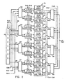
- Fig. 2 illustrates a nominal four megabit memory 24 which can be one quarter of a sixteen megabit memory chip.
- the four megabit or four megacell memory 24 includes eight memory arrays 26, 28, 30, 32, 34, 36, 38 and 40, each having 524, 288 or 512k memory cells with 512 word lines arranged horizontally and 1024 bit or bit/sense lines arranged vertically, as is well known.
- Also shown in Fig. 2 are eight one out of 512 or 1/512 decode circuits 42, 44, 46, 48, 50, 52, 54 and 56 which have outputs coupled to the respective 512k arrays 26, 28, 30, 32, 34, 36, 38 and 40.
- Each of the 1/512 decode circuits is designed to select one of the 512 word lines of its respective 512k array.
- Row addresses RA0 to RA8 from the row address buffer 12 of Fig. 1 are applied to the inputs of each of the 1/512 decode circuits.
- a first plurality of transmission gate systems is indicated at blocks 58, 60, 62 and 64 with each transmission gate system having four inputs and two outputs, with the systems being similar to each other.
- a first output 58a from the transmission gate system 58 is connected to an input of the 1/512 decode circuit 42, with a second output 58b being connected to the 1/512 decode circuit 44, a first output 60a from the transmission gate system 60 is connected to an input of the 1/512 decode circuit 46, with a second output 60b being connected to the 1/512 decode circuit 48, a first output 62a from the transmission gate system 62 is connected to an input of the 1/512 decode circuit 50, with a second output 62b being connected to the 1/512 decode circuit 52, and a first output 64a from the transmission gate system 64 is connected to an input of the 1/512 decode circuit 54, with a second output 64b being connected to the 1/512 decode circuit 56.
- Each of the transmission gate systems 58, 60, 62 and 64 has three inputs connected to respective terminals CBR, TTC and RA11 shown in Fig. 1 of the drawings.
- the fourth input to each of the transmission gate systems 58, 60, 62 and 64 is connected to a different output of a one out of four or 1/4 decode circuit 66 having inputs connected to the row address buffer 12 of Fig. 1 by row address lines RA9 and RA10.
- the outputs of the 1/4 decode circuit 66 are identified by lines 63, 65, 67 and 69, with line 63 being connected to the transmission gate system 58, line 65 being connected to the transmission gate system 60, the line 67 being connected to the transmission gate system 62 and line 69 being connected to the transmission gate system 64.
- Eight one out of 1024 or 1/1024 column decode circuits 68, 70, 72, 74, 76, 78, 80 and 82 are coupled to respective ones of the 512k arrays 26, 28, 30, 32, 34, 36, 38 and 40 and arranged, as is known, to select one of the 1024 bit lines of each of the 512k arrays.
- Each of the 1/1024 column decode circuits 68, 70, 72, 74, 76, 78, 80 and 82 has the column address lines CA0 to CA9 connected to its input.
- a second plurality of transmission gate systems is indicated at 84, 86, 88 and 90 with each of these transmission gate systems having four inputs and an output, with each system of the second plurality of transmission gate systems being similar to each other.
- the first and second inputs of each of the second plurality of transmission gate systems 84, 86, 88 and 90 are connected to the column address line CA10 of the column address buffer 14 and to the 12/10 control line TTC' of the inverter 22 of Fig. 1, respectively.
- Third and fourth inputs 84a and 84b of the transmission gate system 84 are coupled to a selected bit line of the 512k array 26 through the 1/1024 column decode circuit 68 and of the 512k array 28 through the 1/1024 column decode circuit 70, respectively, third and fourth inputs 86a and 86b of the transmission gate system 86 are coupled to a selected bit line of the 512k array 30 through the 1/1024 column decode circuit 72 and of the 512k array 32 through the 1/1024 column decode circuit 74, respectively, third and fourth inputs 88a and 88b of the transmission gate system 88 are coupled to a selected bit line of the 512k array 34 through the 1/1024 column decode circuit 76 and of the 512k array 36 through the 1/1024 column decode circuit 78, respectively, and third and fourth inputs 90a and 90b of the transmission gate system 90 are coupled to a selected bit line of the 512k array 38 through the 1/1024 column decode circuit 80 and of the 512k array 40 through the 1/1024
- each of the transmission gate systems of the second group of transmission gate systems 84, 86, 88 and 90 is connected to an output terminal DQ0 after passing through, e.g., an off-chip driver circuit (not shown). It should be noted that the terminal DQ0 can also serve as an input terminal.
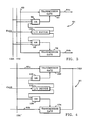
- Fig. 3 of the drawings there is shown a more detailed diagram in block form of one of the transmission gate systems 64 of the first group of transmission gate systems illustrated in Fig. 2.
- the transmission gate system 64 includes first and second transmission gates 92 and 94, respectively, first and second OR gates 96 and 98, respectively, and a one out of two or 1/2 decode circuit 100.
- Both the output CBR from the refresh address counter 20 and the control pulse terminal TTC shown in Fig. 1 are connected to each of the first 96 and second 98 OR gates so as to selectively activate these gates.
- the output line 69 from the 1/4 decode circuit 66 of Fig. 2 is connected to the input of the first transmission gate 92 and to the input of the second transmission gate 94.
- the output from the first transmission gate 92 is connected to the first output 64a of the transmission gate system 64 and the output from the second transmission gate 94 is connected to the second output 64b of the transmission gate system 64.
- Fig. 4 of the drawings there is shown a more detailed diagram in block form of one of the transmission gate systems 90 of the second group of transmission gate systems 84, 86, 88 and 90 illustrated in Fig. 2.
- the transmission gate system 90 includes first and second transmission gates 102 and 104, respectively, first and second OR gates 106 and 108, respectively, and a one out of two or 1/2 decode circuit 110.
- the output TTC' from the inverter 22 shown in Fig. 1 is connected to each of the first and second OR gates 106 and 108 so as to selectively activate these OR gates.
- the first and second transmission gates 102 and 104 is connected to the output terminal DQ0, which, as stated hereinabove, can also be an input terminal.
- circuits illustrated in Figs. 1, 2, 3 and 4 of the drawings will first be described in connection with the 11/11 addressing technique, i.e., when a memory on a chip is arranged to respond to eleven addresses during the row enable (RE) time and eleven addresses during the column enable (CE) time, and then the circuits will be described in connection with the 12/10 addressing technique, i.e., when a memory on a chip is arranged to respond to twelve addresses during the row enable (RE) time and ten addresses during the column enable (CE) time.
- 11/11 addressing technique i.e., when a memory on a chip is arranged to respond to eleven addresses during the row enable (RE) time and eleven addresses during the column enable (CE) time
- 12/10 addressing technique i.e., when a memory on a chip is arranged to respond to twelve addresses during the row enable (RE) time and ten addresses during the column enable (CE) time.
- the voltage on the terminal TTC is set to a high value, such as +3.5 to +5.0 volts, by connecting or wire bonding the terminal TTC to any point of constant high potential on the chip.
- a high value such as +3.5 to +5.0 volts
- the twelve addresses A0 to A11 applied to the chip and indicated in Fig. 1 of the drawings are buffered in the address buffer 10 connected to the row address buffer 12 which provides at the output thereof twelve row addresses RA0 to RA11.
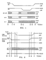
- the areas shown by a series of Xs represent voltages at times, such as between times t0 and t1, which are unimportant to the operation of the circuits or systems of the invention. These areas are commonly called "don't care voltages".
- the row addresses RA9 and RA10 are applied to the 1/4 decode circuit 66 of Fig. 2 to select one of the four outputs 63, 65, 67 and 69.
- the selected output e.g., output 69, has preferably a high voltage which is applied to the transmission gate system 64 and more particularly to the inputs of the first and second transmission gates 92 and 94 shown in Fig. 3 of the drawings. Since the voltage on terminal TTC is high and applied to both of the OR circuits 96 and 98, the output of the OR circuits 96 and 98 activates or turns on both of the transmission gates 92 and 94.
- the high voltage on the output line 69 passes through to the outputs 64a and 64b of the transmission gates 92 and 94, respectively.
- the high voltage on outputs 64a and 64b activates both of the 1/512 decode circuits 54 and 56 and consequently both of the 512k arrays 38 and 40, with the row addresses RA0 to RA8 applied to the 1/512 decode circuits selecting one of the 512 word lines in each of the 512k arrays 38 and 40.
- the twelve addresses A0 through A11 presented to the chip are buffered in the address buffer 10 connected to the column address buffer 14 of Fig. 1 which provides at the output thereof only eleven column addresses CA0 through CA10, with address A11 at RE time being address CA10 at CE time.
- the column addresses CA0 to CA9 are applied to the 1/1024 column decode circuits 68, 70, 72, 74, 76, 78, 80 and 82 to select 1 out of the 1024 bit/sense lines in the activated arrays, i.e., arrays 38 and 40.
- the column address CA10 is applied to transmission gate systems 84, 86, 88 and 90 to select one out of the two outputs from the two selected arrays, i.e., the output 90a from array 38 or output 90b from array 40.
- This one of two select operation in the transmission gate system 90 can better be understood by referring to Fig. 4 of the drawings. As shown in Fig. 4, since the voltage at the terminal TTC has been set to a high value, the voltage on TTC' which is at the output of the inverter 22 shown in Fig. 1 of the drawings, is at a low voltage, thus, the voltage at the outputs of the OR gates 106 and 108 does not activate or turn on the transmission gates 102 and 104.
- the voltage of the column address CA10 is either high or low, which applies an activating voltage to either OR gate 106 or to OR gate 108 to turn on transmission gate 102 or transmission gate 104, respectively. Accordingly, assuming that the transmission gate 102 is selected, a voltage representative of the selected cell in the 512k array 38 of the large memory 24 is applied to the output terminal DQ0 through the output 90a. It should be understood that the terminal DQ0 is used as a data input terminal during a write operation, as well as a data output terminal.
- the voltage on the terminal TTC is set to a low value, such as zero volts, or even to a negative value, by connecting or wire bonding the terminal TTC to any point of constant low potential on this particular memory chip.
- the twelve addresses A0 to A11 applied to the chip and indicated in Fig. 1 of the drawings are buffered in the address buffer 10 connected to the row address buffer 12 which provides at the output twelve row addresses RA0 to RA11.
- the row addresses RA9 and RA10 are applied to the 1/4 decode circuit 66 of Fig. 2 to select one of the four outputs 63, 65, 67 and 69.
- the selected output e.g., again output 69, has a high voltage which is applied to the transmission gate system 64 and more particularly to the inputs of the first and second transmission gates 92 and 94 shown in Fig. 3 of the drawings. Since the voltage on the terminal TTC is low and applied to both of the OR circuits 96 and 98, the outputs of the OR circuits 96 and 98, which are also low, do not activate either of the transmission gates 92 and 94.
- the voltage on line CBR is low except when a refresh operation is taking place in the memory 24.
- row address RA11 is applied to the input of the 1/2 decode circuit 100, one of the two OR gates 96 and 98 will turn on or open its respective transmission gate 92 and 94.
- the first transmission gate 92 will provide a high voltage on the output 64a to activate the 1/512 decode circuit 54 and consequently the 512k array 38, with the row addresses RA0 to RA8 applied to the 1/512 decode circuits selecting one of the 512 word lines in the 512k array 38.
- the twelve addresses A0 to A11 presented to the chip are also buffered in the address buffer 10 connected to the column address buffer 14 of Fig. 1 which provides at the output thereof only eleven column addresses CA0 through CA10.
- the column addresses CA0 to CA9 are applied to the 1/1024 column decode circuits 68, 70, 72, 74, 76, 78, 80 and 82 to select 1 out of the 1024 bit/sense lines in the activated array, i.e., array 38.
- column address CA10 is also applied to the second group of transmission gate systems 84, 86, 88 and 90 when using the 12/10 addressing technique, column address CA10 has no effect on these transmission gate systems since the terminal TTC' is at a high voltage. This can be more clearly understood by referring to Fig. 4 of the drawings wherein the terminal TTC' having a high voltage is connected to both of the OR gates 106 and 108 to activate both transmission gates 102 and 104. Since only the 512 array 38 has been activated, data from the selected cell in array 38 passes through the output 90a through the transmission gate 102 to the output terminal DQ0.
- the refresh address counter 20 supplies a CBR pulse and the addresses RA0 through RA10 to the row address buffer 12.
- CE column enable
- RE row enable
- the use of the 12/10 addressing technique requires that only 1/8 of the chip be powered up which saves active power without impacting either density or performance.
- the use of the 12/10 addressing as such requires a memory cell refresh rate of 4,000 cycles instead of the usual 2,000 cycles when using the 11/11 addressing technique which causes an increase in refresh power to maintain the contents stored in the memory cells valid.
- the typical power difference between a 1/4 array select and a 1/8 array select chip design at 16 million cells or megabits is generally about 150 milliwatts, with a 1/8 array select yielding approximately 350 milliwatts as compared to a 1/4 array select yielding approximately 500 milliwatts.
- the active power yield for a 12/10 addressed chip is about 0.7 of the active power yield for a 11/11 addressed chip.
- the maximum refresh interval of a dynamic random access memory is technology limited. Thus, if this limit is 32 milliseconds and 2,000 refresh cycles are required, then the average time required between refreshes is 32/2048 or 15.7 microseconds and, with a chip cycle of 100 nanoseconds, there is a memory availability of 15.6/15.7 or about 99.3 %. At 4,000 refresh cycles the average time between refreshes becomes 7.85 microseconds and the availability becomes about 98.7 %.
- the power to keep the memory contents valid is as follows:
- KAP Power Active Cycle
- NC No. of Cycles
- RT Refresh Time
- a 12/10 multiplexed address chip requires 1.4 times more power to maintain memory contents valid than does a 11/11 multiplexed address chip.
- the single cycle active power of a 12/10 multiplexed addressed chip is only 0.7 the power of an 11/11 multiplexed addressed chip.
- the availability of a 12/10 multiplexed addressed chip is less than that of an 11/11 multiplexed addressed chip.
- a 2,000 cycle refresh for a chip with 11/11 multiplexed addressing with a 2,000 cycle row enable (RE) only refresh or a 2,000 cycle column address before row address (CBR) refresh and for a chip with a 12/10 multiplexed addressing with a 4,000 cycle row enable (RE) only refresh or with a 2,000 cycle column address before row address (CBR) refresh.
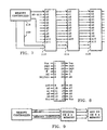
- the circuit illustrated in Fig. 1 of the drawing is required only once on a chip, however, if desired this circuit may be repeated in part or in its entirety for enhancing yield, reliability or performance.
- the output DQ0 is an input/output terminal for the one quadrant illustrated particularly in Fig. 2 of the drawings and that each of the other three quadrants have an input/output terminal which may be identified as DQ1, DQ2 and DQ3 and which are indicated in Fig. 8 of the drawings.
- the same address on address A11 at RE time is also retransmitted on address A10 so as to address the same location in each of the chips in a memory system or card.
- the 11/11 addressed chip uses inputs A0 to A10 and gets the same total 22 addresses as the 12/10 addressed chip.
- the 12/10 addressed chip uses only addresses A0 to A9 at the CE time. Address integrity to the two chips is maintained.
- the system can maintain a low refresh power and high availability with mixed chips on the memory buss by using the CBR voltage refresh technique at 2,000 cycles, but an RE only refresh is still available by cycling at 4,000 cycles during the refresh interval and supplying the proper addresses A0 to A11.
- memory chips 112, 114 and 116 receive their addresses from a memory controller 118 along common address lines A0 to A11 except that address line A11 is not connected to the memory chip 114 since it is operated by the 11/11 multiplexed addresses, whereas the memory chips 112 and 116 are operated by the 12/10 multiplexed addresses.
- the outputs 120 from the memory controller 118 provide controls for timing and chip selection, as is known.
- the packaged unit could provide either the extra two inputs A11 and TTC for card programming by card wiring or the same lead frame could be used with a simple two wire bond change, one to bias TTC and one to connect the address A11 to provide industry standard X4 pinouts.
- FIG. 8 of the drawings An industry type package is indicated in Fig. 8 of the drawings having 24 terminals or pins, with locations 7, 8, 21 and 22 not being provided normally with terminals or pins.
- the Vcc pin is for the positive voltage supply
- Vss is the low voltage or ground
- DQ0, DQ1, DQ2 and DQ3 are the inputs/output terminals of the respective four quadrants of the memory
- W is the write/read control
- G is an output enable voltage
- NC is generally a no connect or not used pin.
- Fig. 9 indicates how a 16 megabit memory chip using the 12/10 addressing technique can be added to an existing memory system, using the 11/11 addressing technique, essentially by merely adding a memory chip arranged in accordance with the design of the present invention and adding a twelfth address from the memory controller.
- the present invention provides a memory system with optimum addressing for any particular application including the use of 11/11 or 12/10 addressing, column enable (CE) before row enable (RE) refreshing at 2,000 cycles, RE only refreshing for 11/11 addressing or 4,000 cycle refreshing for 12/10 addressing, with card wiring to support either the 11/11 or 12/10 addressing depending on part availability and mixing both 11/11 and 12/10 addressing on the same card or system.
Landscapes
- Engineering & Computer Science (AREA)
- Microelectronics & Electronic Packaging (AREA)
- Dram (AREA)
- Static Random-Access Memory (AREA)
Claims (13)
- Ein dynamisches Speichersystem mit einer Vielzahl von Speichersegmenten (26, 28, 30, 32, 34, 36, 38) verschaltet in einer Vielzahl von Bitleitungen und Wortleitungen, mit einer Vielzahl von Wort-Decodierern (42, 44, 46, 48, 50, 52, 54, 56), die eine erste Anzahl von Adressenbits zum Anwählen einer der Vielzahl von Wortleitungen aufnehmen, und mit einer Vielzahl von Bit-Decodierern (68, 70, 72, 74, 76, 78, 80, 82), die eine zweite Anzahl von Adressenbits zum Anwählen einer der Vielzahl von Bitleitungen aufnehmen,gekennzeichnet durch:Einschalt/Auschaltmittel, die mit den Eingängen der Vielzahl von Wortdecodierern (42, 44, 46, 48, 50, 52, 54, 56) und der Vielzahl von Bit-Decodierern (68, 70, 72, 74, 76, 78, 80, 82) zum Ausschalten gewisser vorgewählter Wort-Decodierer (42, 44, 46, 48, 50, 52, 54, 56) und zum Einschalten gewisser vorgewählter Bit-Decodierer (68, 70, 72, 74, 76, 78, 80, 82) wenn ein externes Steuersignal eine erste vorgegebene Beziehung zwischen der Bitlänge der Zeilenadresse und der Spaltenadresse in einem gegebenen Speichersystem-Betriebszyklus anzeigt, und zum Ausschalten vorgewählter Bit-Decodierer (68, 70, 72, 74, 76, 78, 80, 82) und Einschalten gewisser vorgewählter Wort-Decodierer (42, 44, 46, 48, 50, 52, 54, 56), wenn das externe Steuersignal eine zweite vorgegebene Beziehung zwischen der Bitlänge der Zeilenadresse und der Spaltenadresse in dem gegebenen Speichersystem-Betriebszyklus anzeigt.
- Das Speichersystem gemäß Anspruch 1, in dem die Einschalt/Ausschaltmittel umfassen:Eine erste Vielzahl von Transmissionsgattersystemen (58, 60, 62, 64) mit jeweils ersten (92) und zweiten (94) Transmissionsgattern, wobei jedes der Gatter mit einem Eingang an einen anderen dieser Vielzahl von Wort-Decodierern (42, 44, 46, 48, 50, 52, 54, 56) gekoppelt ist,ein zweites Decodiermittel (66) mit einer ersten Vielzahl von Ausgängen, wobei jeder der Ausgänge an ein entsprechendes der ersten Vielzahl von Transmissionsgattersystemen (58, 60, 62, 64) gekoppelt ist,erste Mittel (96, 98, 100) zur wahlweisen Aktivierung der ersten (92) und zweiten (94) Gatter in jedem der ersten Vielzahl von Transmissionsgattersystemen (58, 60, 62, 64),eine zweite Vielzahl von Transmissionsgattersystemen (84, 86, 88, 90) mit jeweils ersten (102) und zweiten (104) Transmissionsgattern, wobei jedes der Gatter der zweiten Vielzahl von Transmissionsgattersystemen (84, 86, 88, 90) an einen anderen dieser Vielzahl von Bit-Decodierern (68, 70, 72, 74, 76, 78, 80, 82) gekoppelt ist, undMittel (106, 108, 110) zur wahlweisen Aktivierung der ersten (102) und zweiten (104) Transmissionsgatter in jedem der zweiten Vielzahl von Transmissionsgattersystemen (84, 86, 88, 90).
- Das Speichersystem gemäß Anspruch 2, wobei jedes der Transmissionsgattersysteme ferner eine Eins-von-Zwei-Decodierschaltung (100, 110) beinhaltet mit einem ersten Ausgang, der am ersten Transmissionsgatter (92, 102) liegt, und mit einem zweiten Ausgang, der am zweiten Transmissionsgattersystem (94, 104) jeweils des entsprechenden Transmissionsgattersystems liegt.
- Das Speichersystem gemäß Anspruch 3, wobei jedes der Transmissionsgattersysteme ferner beinhaltet ein erstes (96, 106) und ein zweites (98, 108) ODER-Gatter, wobei der erste Ausgang der Eins-von-Zwei-Decodierschaltung über das erste ODER-Gatter (96, 106) an das erste Transmissionsgatter (92, 102) gekoppelt ist, und der zweite Ausgang der Eins-von-Zwei-Decodierschaltung über das zweite ODER-Gatter (98, 108) an das zweite Transmissionsgatter (94, 104) gekoppelt ist.
- Das Speichersystem gemäß Anspruch 4, wobei das erste und das zweite Mittel Mittel zum Anlegen von Speicheradressenimpulsen (RA11, CA10) an Eingänge der Eins-von-Zwei-Decodierschaltungen (100, 110) sowie Mittel zum Anlegen fester Spannungen (CBR, TTC, TTC') an Eingänge der ODER-Gatter beinhaltet.
- Das Speichersystem gemäß Anspruch 5, wobei das erste Mittel der ersten Vielzahl von Transmissionsgattersystemen ferner Mittel zum wahlweisen Anlegen eines Impulses zum Spalteneinschalten vor dem Zeileneinschalten an einen Eingang jedes der ODER-Gatter beinhaltet.
- Das Speichersystem gemäß Anspruch 2, wobei das erste Mittel Zeilenadressenmittel (12), einen Wiederholungszähler (20) und einen Anschluß mit einer Wirkspannung (TTC) beinhaltet, und das zweite Mittel Spaltenadressenmittel (14) und einen Anschluß mit einer Komplementärspannung (TTC') der Wirkspannung (TTC) beinhaltet.
- Das Speichersystem gemäß Anspruch 2, wobei jedes der ersten Vielzahl von Transmissionsgattersystemen (58, 60, 62, 64) ferner beinhaltet ein erstes (96) und ein zweites (98) ODER-Gatter, wobei das erste ODER-Gatter (96) einen Ausgang aufweist, der an das erste Transmissionsgatter (92) angeschlossen ist, und das zweite ODER-Gatter (98) einen Ausgang aufweist, der an das zweite Transmissionsgatter (94) angeschlossen ist, und eine Eins-von-Zwei-Decodierschaltung (100) einen ersten Ausgang aufweist, der an einen Eingang des ersten ODER-Gatters (96) angeschlossen ist, und einen zweiten Ausgang aufweist, der an einen Eingang des zweiten ODER-Gatters (98) angeschlossen ist.
- Das Speichersystem gemäß Anspruch 2, wobei jedes der zweiten Vielzahl von Transmissionsgattersystemen (84, 86, 88, 90) ferner beinhaltet ein erstes (106) und ein zweites (108) ODER-Gatter, wobei das erste ODER-Gatter (106) einen Ausgang aufweist, der an das erste Transmissionsgatter (102) angeschlossen ist, und das zweite ODER-Gatter (108) einen Ausgang aufweist, der an das zweite Transmissionsgatter (104) angeschlossen ist, und eine Eins-von-Zwei-Decodierschaltung (110) einen ersten Ausgang aufweist, der an einen Eingang des ersten ODER-Gatters (106) angeschlossen ist, und einen zweiten Ausgang aufweist, der an einen Eingang des zweiten ODER-Gatters (108) angeschlossen ist, wobei die Ausgänge dieses ersten und zweiten Transmissionsgatters an einen gemeinsamen Punkt (DQ0) gelegt sind.
- Das Speichersystem gemäß Anspruch 8, wobei jedes der zweiten Vielzahl von Transmissionsgattersystemen (84, 86, 88, 90) ferner beinhaltet ein erstes (106) und ein zweites (108) ODER-Gatter, wobei das erste ODER-Gatter (106) einen Ausgang aufweist, der an das erste Transmissionsgatter (102) angeschlossen ist, und das zweite ODER-Gatter (108) einen Ausgang aufweist, der an das zweite Transmissionsgatter (104) angeschlossen ist, und eine Eins-von-Zwei-Decodierschaltung (110) einen ersten Ausgang aufweist, der an einen Eingang des ersten ODER-Gatters (106) angeschlossen ist, und einen zweiten Ausgang aufweist, der an einen Eingang des zweiten ODER-Gatters (108) angeschlossen ist.
- Das Speichersystem gemäß Anspruch 8, wobei das erste Mittel Mittel (12) zum Anlegen von Zeilenadressenimpulsen (RA11) an einen Eingang der Eins-von-Zwei-Decodierschaltungen (100), Mittel zum Anlegen einer ersten Festspannung (TTC) an Eingänge der ODER-Gatter (96, 98), sowie Mittel (20) zum Anlegen von Signalen (CBR) von einem Wiederholadressenzähler an Eingänge der ODER-Gatter (96, 98) beinhaltet.
- Das Speichersystem gemäß Anspruch 9 oder 10, wobei das zweite Mittel Mittel (14) zum Anlegen von Spaltenadressenimpulsen (CA10) an einen Eingang der Eins-von-Zwei-Decodierschaltung (110), Mittel zum Anlegen einer zweiten Festspannung (TTC') einer Größe, die sich von der der ersten Festspannung unterscheidet, an Eingänge der ODER-Gatter (106, 108) beinhaltet.
- Das Speichersystem gemäß Anspruch 12, das ferner beinhaltet eine Umkehrstufe (22) mit einem Eingang und einem Ausgang, wobei am Eingang der Umkehrstufe eine erste Festspannung (TTC) liegt und am Ausgang der Umkehrstufe die zweite Festspannung (TTC') steht.
Applications Claiming Priority (2)
| Application Number | Priority Date | Filing Date | Title |
|---|---|---|---|
| US07/479,137 US4999815A (en) | 1990-02-13 | 1990-02-13 | Low power addressing systems |
| US479137 | 1990-02-13 |
Publications (3)
| Publication Number | Publication Date |
|---|---|
| EP0442283A2 EP0442283A2 (de) | 1991-08-21 |
| EP0442283A3 EP0442283A3 (en) | 1992-10-28 |
| EP0442283B1 true EP0442283B1 (de) | 1996-05-08 |
Family
ID=23902797
Family Applications (1)
| Application Number | Title | Priority Date | Filing Date |
|---|---|---|---|
| EP91100624A Expired - Lifetime EP0442283B1 (de) | 1990-02-13 | 1991-01-19 | Adressierungsanordnungen mit niedriger Leistung |
Country Status (4)
| Country | Link |
|---|---|
| US (1) | US4999815A (de) |
| EP (1) | EP0442283B1 (de) |
| JP (1) | JPH0734310B2 (de) |
| DE (1) | DE69119258T2 (de) |
Families Citing this family (3)
| Publication number | Priority date | Publication date | Assignee | Title |
|---|---|---|---|---|
| US5134616A (en) * | 1990-02-13 | 1992-07-28 | International Business Machines Corporation | Dynamic ram with on-chip ecc and optimized bit and word redundancy |
| US5590071A (en) * | 1995-11-16 | 1996-12-31 | International Business Machines Corporation | Method and apparatus for emulating a high capacity DRAM |
| CN109213774B (zh) * | 2018-08-01 | 2024-03-08 | 平安科技(深圳)有限公司 | 数据的存储方法及装置、存储介质、终端 |
Family Cites Families (5)
| Publication number | Priority date | Publication date | Assignee | Title |
|---|---|---|---|---|
| JPS573289A (en) * | 1980-06-04 | 1982-01-08 | Hitachi Ltd | Semiconductor storing circuit device |
| JPS61294562A (ja) * | 1985-06-21 | 1986-12-25 | Mitsubishi Electric Corp | 半導体記憶装置 |
| JPS63133395A (ja) * | 1986-11-25 | 1988-06-06 | Toshiba Corp | 半導体記憶装置 |
| US4796227A (en) * | 1987-03-17 | 1989-01-03 | Schlumberger Systems And Services, Inc. | Computer memory system |
| US4843261A (en) * | 1988-02-29 | 1989-06-27 | International Business Machines Corporation | Complementary output, high-density CMOS decoder/driver circuit for semiconductor memories |
-
1990
- 1990-02-13 US US07/479,137 patent/US4999815A/en not_active Expired - Fee Related
-
1991
- 1991-01-18 JP JP3016900A patent/JPH0734310B2/ja not_active Expired - Lifetime
- 1991-01-19 EP EP91100624A patent/EP0442283B1/de not_active Expired - Lifetime
- 1991-01-19 DE DE69119258T patent/DE69119258T2/de not_active Expired - Lifetime
Also Published As
| Publication number | Publication date |
|---|---|
| JPH05198173A (ja) | 1993-08-06 |
| US4999815A (en) | 1991-03-12 |
| DE69119258D1 (de) | 1996-06-13 |
| DE69119258T2 (de) | 1996-11-21 |
| EP0442283A3 (en) | 1992-10-28 |
| EP0442283A2 (de) | 1991-08-21 |
| JPH0734310B2 (ja) | 1995-04-12 |
Similar Documents
| Publication | Publication Date | Title |
|---|---|---|
| US5862095A (en) | Semiconductor memory having both a refresh operation cycle and a normal operation cycle and employing an address non-multiplex system | |
| US5590071A (en) | Method and apparatus for emulating a high capacity DRAM | |
| EP0640980B1 (de) | Halbleiterspeicher mit mehreren Banken | |
| EP0563082B1 (de) | Synchrone auffrischung eines dynamischen ram-speichers | |
| US5644541A (en) | Memory substitution system and method for correcting partially defective memories | |
| US5848006A (en) | Redundant semiconductor memory device using a single now address decoder for driving both sub-wordlines and redundant sub-wordlines | |
| US6240039B1 (en) | Semiconductor memory device and driving signal generator therefor | |
| US5251178A (en) | Low-power integrated circuit memory | |
| US20030145163A1 (en) | Electronic system and refresh method | |
| US5446692A (en) | Semiconductor memory device having redundancy memory cells shared among memory blocks | |
| US4241425A (en) | Organization for dynamic random access memory | |
| US5327389A (en) | Semiconductor memory device having a block selection function with low power consumptions | |
| US5966316A (en) | Semiconductor memory device having storage capacity of 22N+1 bits | |
| US5280451A (en) | Signature circuit for non-volatile memory device | |
| US5995427A (en) | Semiconductor memory device having test mode | |
| US6208569B1 (en) | Method of and apparatus for sharing redundancy circuits between memory arrays within a semiconductor memory device | |
| US4578780A (en) | Dual port type semiconductor memory | |
| US5305274A (en) | Method and apparatus for refreshing a dynamic random access memory | |
| US6337820B1 (en) | Dynamic memory device performing stress testing | |
| JP3018498B2 (ja) | 半導体記憶装置 | |
| KR100294965B1 (ko) | 입/출력장치의구성방법및그회로 | |
| US4934826A (en) | Block partitioned dynamic semiconductor memory device | |
| EP0953912B1 (de) | Halbleiterspeicheranordnung mit Redundanz | |
| EP0442283B1 (de) | Adressierungsanordnungen mit niedriger Leistung | |
| US6304498B1 (en) | Semiconductor memory device capable of suppressing degradation in operation speed after replacement with redundant memory cell |
Legal Events
| Date | Code | Title | Description |
|---|---|---|---|
| PUAI | Public reference made under article 153(3) epc to a published international application that has entered the european phase |
Free format text: ORIGINAL CODE: 0009012 |
|
| AK | Designated contracting states |
Kind code of ref document: A2 Designated state(s): DE FR GB |
|
| 17P | Request for examination filed |
Effective date: 19911211 |
|
| PUAL | Search report despatched |
Free format text: ORIGINAL CODE: 0009013 |
|
| AK | Designated contracting states |
Kind code of ref document: A3 Designated state(s): DE FR GB |
|
| 17Q | First examination report despatched |
Effective date: 19941117 |
|
| GRAH | Despatch of communication of intention to grant a patent |
Free format text: ORIGINAL CODE: EPIDOS IGRA |
|
| GRAA | (expected) grant |
Free format text: ORIGINAL CODE: 0009210 |
|
| AK | Designated contracting states |
Kind code of ref document: B1 Designated state(s): DE FR GB |
|
| REF | Corresponds to: |
Ref document number: 69119258 Country of ref document: DE Date of ref document: 19960613 |
|
| ET | Fr: translation filed | ||
| PG25 | Lapsed in a contracting state [announced via postgrant information from national office to epo] |
Ref country code: GB Effective date: 19970119 |
|
| PLBE | No opposition filed within time limit |
Free format text: ORIGINAL CODE: 0009261 |
|
| STAA | Information on the status of an ep patent application or granted ep patent |
Free format text: STATUS: NO OPPOSITION FILED WITHIN TIME LIMIT |
|
| 26N | No opposition filed | ||
| GBPC | Gb: european patent ceased through non-payment of renewal fee |
Effective date: 19970119 |
|
| PG25 | Lapsed in a contracting state [announced via postgrant information from national office to epo] |
Ref country code: FR Effective date: 19970930 |
|
| REG | Reference to a national code |
Ref country code: FR Ref legal event code: ST |
|
| PGFP | Annual fee paid to national office [announced via postgrant information from national office to epo] |
Ref country code: DE Payment date: 19990127 Year of fee payment: 9 |
|
| PG25 | Lapsed in a contracting state [announced via postgrant information from national office to epo] |
Ref country code: DE Free format text: LAPSE BECAUSE OF THE APPLICANT RENOUNCES Effective date: 20000113 |