EP0440624B1 - Verfahren zur verarbeitung von gesendeten und reflektierten signalen und zur störsignalunterdrückung der gesuchten signale - Google Patents
Verfahren zur verarbeitung von gesendeten und reflektierten signalen und zur störsignalunterdrückung der gesuchten signale Download PDFInfo
- Publication number
- EP0440624B1 EP0440624B1 EP89904622A EP89904622A EP0440624B1 EP 0440624 B1 EP0440624 B1 EP 0440624B1 EP 89904622 A EP89904622 A EP 89904622A EP 89904622 A EP89904622 A EP 89904622A EP 0440624 B1 EP0440624 B1 EP 0440624B1
- Authority
- EP
- European Patent Office
- Prior art keywords
- signals
- signal
- transponder
- binary
- reflected
- Prior art date
- Legal status (The legal status is an assumption and is not a legal conclusion. Google has not performed a legal analysis and makes no representation as to the accuracy of the status listed.)
- Expired - Lifetime
Links
Images


Classifications
-
- G—PHYSICS
- G01—MEASURING; TESTING
- G01S—RADIO DIRECTION-FINDING; RADIO NAVIGATION; DETERMINING DISTANCE OR VELOCITY BY USE OF RADIO WAVES; LOCATING OR PRESENCE-DETECTING BY USE OF THE REFLECTION OR RERADIATION OF RADIO WAVES; ANALOGOUS ARRANGEMENTS USING OTHER WAVES
- G01S13/00—Systems using the reflection or reradiation of radio waves, e.g. radar systems; Analogous systems using reflection or reradiation of waves whose nature or wavelength is irrelevant or unspecified
- G01S13/74—Systems using reradiation of radio waves, e.g. secondary radar systems; Analogous systems
- G01S13/79—Systems using random coded signals or random pulse repetition frequencies, e.g. "Separation and Control of Aircraft using Non synchronous Techniques" [SECANT]
Definitions
- the invention relates to a method for handling signals in an identification system, as described in the introduction to claim 1.
- the invention is intended for use in an identification system, which consists of a transmitter, a mobile, binary-coded passive, the identification-providing answering device (transponder) and a receiver unit, which in combination form a treatment system.
- the transponder can be implemented using SAW (Surface Acoustic Wave) technology.
- SAW Surface Acoustic Wave
- Transponders using this technology have many advantages for such an application; they are inexpensive, easy to manufacture and require no maintenance, and they are independent of external energy sources, etc.
- a transpoder according to this technology has a characteristic which has a fundamental disadvantage: the high insertion loss. This means that the reflected Return signal is weak in relation to the incoming interrogation pulse. This disadvantage is exacerbated by the fact that the transmitter unit uses a weak output radar in order to meet the radiation requirements for the frequency used.
- the result is such that the strength of the desired return signal to the receiver unit of the system is very small in relation to the unwanted signals, the noise and the self-noise of the receiver itself.
- the traditional method for treating signals to improve the signal-to-noise ratio for the applications mentioned is to digitize the reflected signal directly by means of A / D (analog / digital) converters and to have digital processing connected to it. Processing is performed by averaging the digital values of the analog signals over multiple repeated return signal passes. This improves the signal-to-noise ratio because the desired signal is the same in each pass, while the noise is different.
- this method requires a powerful digital processing unit. The unit must operate quickly and have significant computing power to average an appropriate number of passes.
- the A / D converter must be one of the fastest and most advanced designs available. This solution means that the technology used clearly sets limits on how efficient the process is. This will also require the use of expensive digital processors and A / D converters.
- Another method used in radar technology uses delay lines so that a signal is delayed by one pass and averaged by adding these signals in an analog manner. This method has a limitation because the number of averages that can be carried out is very limited and there is no synchronization with the (signal) run.
- US Pat. No. 3,706,094 describes a receiver for a low output radar surveillance system, in which the receiver is equipped for analog processing of the received returning pulse signals, each of which is divided by a certain number of temporal signals Interruptions in controlled gate circuits and in which the signal from each gate circuit is fed to an integrator for the repeated integration of the pulse signals, the repetition frequency of the pulse signals being considerably higher than the limit frequency of the low-pass filter of the integrator.
- the pulse signal can be reconstructed by reading the output of the integrator from the receiver.
- the main aim of the present invention is to develop a safe method for recognizing a radar signal which is reflected by a passive, coded transponder with phase modulation of the transmitted signal. - This can be achieved by using the method according to claim 1. Other aspects of the invention are set out in the remaining claims.
- the present invention can be distinguished from the technique of the mentioned patent by the fact that the present invention employs a cooperation between the transmitted and reflected signals. This is done by means of a binary, digital random sequence that modulates the transmitted signal, and application of the same random sequence for recognizing the demodulated, reflected signal. A large number of phase-modulated pulse sequences are generated, which are preferably different. This is accomplished by splitting the binary random sequence mentioned above and using these splits of the binary random sequence to match the demodulated, reflected signal Feed storage medium such as an integrator chain, which is designed such that the (storage) medium contains values corresponding to the desired signals, while unwanted signals and noise are largely reduced.
- the technology used in the context of the invention consists of analog averaging (averaging) of the signal before it is digitized.
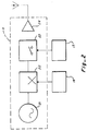
- the embodiment according to Figure 1 consists of a transmitter 11, a transponder 12 which e.g. could be a passive SAW transponder and a receiver 13 which is connected to an integrator arrangement 16 of integrator sections 37.
- a device 14 generates a binary random sequence which is passed to the transmitter 11 and a sieve register 17 which is connected to the integrator arrangement 16.
- a device 15 outputs a signal with time limits (time interval signal), which is fed to the transmitter 11 and the shift register 17.
- the transmitter 11 transmits a phase-modulated pulse sequence which is received and reflected by the encoded transponder 12, so that the reflected signal consists of series of pulse sequences and spaces without pulse sequences, which together form an identity which is identical to the transponder code.
- the desired signal is received by the receiver 13, which is then demodulated and sent to an integrator arrangement 16, which is controlled by the above-mentioned binary sequence from the submission 14 together with the temporal interruptions determined by the device 15.
- FIG. 2 shows a more detailed reproduction of the transmitter.
- This consists of an oscillator 21, which forms a fixed frequency signal.
- This fixed frequency signal is phase-modulated by the binary random sequence of the device 14.
- the signal modulated in the device 22 is divided into pulse sequences by means of a gate circuit 23 which is controlled by the time interval signal of the device 15.
- the pulse sequences are then amplified by an amplifier 24 before transmission.
- FIG 3 shows a more detailed representation of the receiver 13 and the decoder unit.
- the signal is demodulated in the receiver 13 into a time and phase-coded signal 31A, which is superimposed by unwanted noise.
- the signal 31A arrives at a switch 36A which directs the signal 31A into an integrator section 37 of the integrator arrangement 16.
- This integrator section 37 can e.g. be an RC filter with a large time constant compared to the individual signal run (e.g. 10000x larger).
- the binary sequence of the device 14 and the time interval signal of the device 15 form the input signals for an AND gate 32A, the output signal of which is fed to a shift register 33A, to which the same binary sequence as is used in the transmitter is then fed to form the phase-modulated pulse sequence .
- This binary sequence is clock driven by the shift register 33A using an external clock signal (not shown in the drawing). It is possible to obtain a signal from different positions in the shift register 33A, for example after certain time intervals after the output signal mentioned has been passed into the shift register 33A.
- the signal is removed from the shift register 33A and used to control the switch 36A, which opens or closes for forwarding the demodulated signal 31A from the receiver 13 to the integrator section 37.
- the signal 31A can be inverted by means of an inverter 34 to a signal 31B, which is also fed to the integrator section 37. This is achieved by passing the binary random sequence via an inverter 35 to a shift register 33B and removing it in a position corresponding to the first shift register 33A and controlling the switch 36B in such a way that it opens or closes for the inverted signal 31B in the integrator section 37.
- Both switches 36A and 36B can e.g. controlled such that a logic "1" in the binary sequence opens the switch for the non-inverted signal 31A from the receiver and closes the switch for the inverted signal 31B; if a logical "0" appears in the binary sequence, the opposite will happen.
- the AND gates 32A and 32B will always have a logic "0" at their output, which ensures is that both switches 36A and 36B are open to prevent undesired noise from being applied to integrator section 37.
- the integrator arrangement 16 is formed by a number of integrator sections 37, which are typically the same as the number of "bits” or a multiple of the number of "bits" of the transponder 12.
- the individual integrator sections 37 can be read out whenever the required number of pulse sequences has been processed. This reading can take place asynchronously, without previous events having to be given any attention.
- FIG. 4 shows in chronological representation how two pulse sequences are transmitted by the transmitter 11 and reflected by the transponder 12, in an embodiment in which the transponder 12 has a resolution of four "bits".
- the transponder 12 is encoded with the binary sequence (bit sequence) 1101.
- the first pulse sequence 41A is a phase-modulated signal which is modulated by the first part of a binary random sequence of the device 14, with a length which is determined by the time intervals formed by the device 15.
- the first pulse sequence 41A is received and reflected by the transponder 12, where it is coded for a logic "1". Because the transponder has code 1101 in this example, the reflected signal forms a pattern as shown at 41B where "bit 1", "bit 2" and "bit 4" reflect a pulse train while "bit 3", which has the value of logic "0" does not reflect a signal.
- the reflected pulse trains 41B can and will overlap in the various mutual positions without this having any negative consequences on the result.
- the second pulse train is sent.
- This pulse sequence is phase-modulated by another part of the binary random sequence, which is different from that in the first pulse sequence, and is activated by the device 14 for a certain period of time, which is determined by time interval signals coming from the device 15.
- This second pulse sequence 42A is then reflected by the transponder 12 as in the first case, so that a series of reflected pulse sequences 42B is formed.
- each phase-modulated, corresponding pulse train can be transmitted, reflected and fed to the integrator arrangement 16, so that the desired signal is averaged and most undesirable signals, which are random and asynchronous be reduced.
Applications Claiming Priority (3)
| Application Number | Priority Date | Filing Date | Title |
|---|---|---|---|
| NO884784 | 1988-10-27 | ||
| NO884784A NO169983C (no) | 1988-10-27 | 1988-10-27 | Framgangsmaate og anordning for individuell identifikasjon |
| PCT/NO1989/000034 WO1990004794A1 (en) | 1988-10-27 | 1989-04-24 | Method for processing transmitted and reflected signals for removing unwanted signals and noise from wanted signals |
Publications (2)
| Publication Number | Publication Date |
|---|---|
| EP0440624A1 EP0440624A1 (en) | 1991-08-14 |
| EP0440624B1 true EP0440624B1 (de) | 1996-01-24 |
Family
ID=19891368
Family Applications (1)
| Application Number | Title | Priority Date | Filing Date |
|---|---|---|---|
| EP89904622A Expired - Lifetime EP0440624B1 (de) | 1988-10-27 | 1989-04-24 | Verfahren zur verarbeitung von gesendeten und reflektierten signalen und zur störsignalunterdrückung der gesuchten signale |
Country Status (12)
| Country | Link |
|---|---|
| US (1) | US5144313A (no) |
| EP (1) | EP0440624B1 (no) |
| JP (1) | JPH04502059A (no) |
| AT (1) | ATE133496T1 (no) |
| AU (1) | AU625991B2 (no) |
| CA (1) | CA1337829C (no) |
| DE (1) | DE58909583D1 (no) |
| DK (1) | DK74891A (no) |
| ES (1) | ES2016047A6 (no) |
| FI (1) | FI102418B (no) |
| NO (1) | NO169983C (no) |
| WO (1) | WO1990004794A1 (no) |
Families Citing this family (32)
| Publication number | Priority date | Publication date | Assignee | Title |
|---|---|---|---|---|
| US5231400A (en) * | 1992-05-12 | 1993-07-27 | Unisys Corporation | Covert electronic battlefield identification system |
| US5365551A (en) * | 1992-12-15 | 1994-11-15 | Micron Technology, Inc. | Data communication transceiver using identification protocol |
| US5500650A (en) * | 1992-12-15 | 1996-03-19 | Micron Technology, Inc. | Data communication method using identification protocol |
| US7158031B2 (en) | 1992-08-12 | 2007-01-02 | Micron Technology, Inc. | Thin, flexible, RFID label and system for use |
| US5557280A (en) * | 1992-08-26 | 1996-09-17 | British Technology Group Limited | Synchronized electronic identification system |
| US20050040961A1 (en) * | 1995-04-11 | 2005-02-24 | Tuttle John R. | RF identification system with restricted range |
| US6097301A (en) * | 1996-04-04 | 2000-08-01 | Micron Communications, Inc. | RF identification system with restricted range |
| US5349355A (en) * | 1993-01-21 | 1994-09-20 | The United States Of America As Represented By The Secretary Of The Navy | Credential tracking system |
| KR20000049066A (ko) * | 1996-10-17 | 2000-07-25 | 핀포인트 코포레이션 | 물품검색 시스템 |
| US6812824B1 (en) | 1996-10-17 | 2004-11-02 | Rf Technologies, Inc. | Method and apparatus combining a tracking system and a wireless communication system |
| US6107910A (en) | 1996-11-29 | 2000-08-22 | X-Cyte, Inc. | Dual mode transmitter/receiver and decoder for RF transponder tags |
| US6114971A (en) | 1997-08-18 | 2000-09-05 | X-Cyte, Inc. | Frequency hopping spread spectrum passive acoustic wave identification device |
| US5986382A (en) | 1997-08-18 | 1999-11-16 | X-Cyte, Inc. | Surface acoustic wave transponder configuration |
| US6060815A (en) | 1997-08-18 | 2000-05-09 | X-Cyte, Inc. | Frequency mixing passive transponder |
| US6208062B1 (en) * | 1997-08-18 | 2001-03-27 | X-Cyte, Inc. | Surface acoustic wave transponder configuration |
| US6339385B1 (en) | 1997-08-20 | 2002-01-15 | Micron Technology, Inc. | Electronic communication devices, methods of forming electrical communication devices, and communication methods |
| US6118789A (en) | 1998-02-19 | 2000-09-12 | Micron Technology, Inc. | Method of addressing messages and communications system |
| US6072801A (en) | 1998-02-19 | 2000-06-06 | Micron Technology, Inc. | Method of addressing messages, method of establishing wireless communications, and communications system |
| USRE43382E1 (en) | 1998-02-19 | 2012-05-15 | Round Rock Research, Llc | Method of addressing messages and communications systems |
| US6061344A (en) | 1998-02-19 | 2000-05-09 | Micron Technology, Inc. | Method of addressing messages and communications system |
| US6275476B1 (en) * | 1998-02-19 | 2001-08-14 | Micron Technology, Inc. | Method of addressing messages and communications system |
| US6714121B1 (en) * | 1999-08-09 | 2004-03-30 | Micron Technology, Inc. | RFID material tracking method and apparatus |
| US7054348B2 (en) * | 2001-11-15 | 2006-05-30 | Koninklijke Philips Electronic N.V. | Using real random number generator as proof of time |
| US7420458B1 (en) | 2004-01-20 | 2008-09-02 | Charles A. Eldering | Secondary card reader |
| US7298264B1 (en) | 2004-01-20 | 2007-11-20 | Charles A. Eldering | RFID tag filtering and monitoring |
| TW200616405A (en) * | 2004-09-30 | 2006-05-16 | Synaptic Lab Ltd | Method of and apparatus for partitioning of a bitstream |
| US7973644B2 (en) * | 2007-01-30 | 2011-07-05 | Round Rock Research, Llc | Systems and methods for RFID tag arbitration where RFID tags generate multiple random numbers for different arbitration sessions |
| US20080212303A1 (en) * | 2007-03-02 | 2008-09-04 | Warren Farnworth | Device for reducing or preventing exchange of information |
| US8134452B2 (en) * | 2007-05-30 | 2012-03-13 | Round Rock Research, Llc | Methods and systems of receiving data payload of RFID tags |
| US9442189B2 (en) * | 2010-10-27 | 2016-09-13 | The Fourth Military Medical University | Multichannel UWB-based radar life detector and positioning method thereof |
| US8576114B2 (en) * | 2011-06-24 | 2013-11-05 | Thales Canada Inc. | Location of a transponder center point |
| CN112098927B (zh) * | 2020-08-19 | 2022-06-21 | 中国电子科技集团公司第二十九研究所 | 一种基于信号合成的多信道测向方法 |
Family Cites Families (7)
| Publication number | Priority date | Publication date | Assignee | Title |
|---|---|---|---|---|
| US3663935A (en) * | 1967-06-05 | 1972-05-16 | Hughes Aircraft Co | Pulse compression code sequencing system |
| US3691557A (en) * | 1969-09-22 | 1972-09-12 | James Nickolas Constant | System for identifying objects using an encoding array for each object |
| US3706094A (en) * | 1970-02-26 | 1972-12-12 | Peter Harold Cole | Electronic surveillance system |
| FR2248517B1 (no) * | 1973-10-23 | 1978-08-04 | Sercel Rech Const Elect | |
| GB1605271A (en) * | 1975-04-03 | 1987-06-10 | Secr Defence | Radio signalling equipment |
| US4015259A (en) * | 1975-05-21 | 1977-03-29 | The United States Of America As Represented By The Secretary Of The Army | Method and apparatus for interrogating and identifying fixed or moving targets |
| US4725841A (en) * | 1983-06-30 | 1988-02-16 | X-Cyte, Inc. | System for interrogating a passive transponder carrying phase-encoded information |
-
1988
- 1988-10-27 NO NO884784A patent/NO169983C/no not_active IP Right Cessation
-
1989
- 1989-04-24 AU AU34185/89A patent/AU625991B2/en not_active Ceased
- 1989-04-24 WO PCT/NO1989/000034 patent/WO1990004794A1/en active IP Right Grant
- 1989-04-24 JP JP1504213A patent/JPH04502059A/ja active Pending
- 1989-04-24 AT AT89904622T patent/ATE133496T1/de not_active IP Right Cessation
- 1989-04-24 EP EP89904622A patent/EP0440624B1/de not_active Expired - Lifetime
- 1989-04-24 DE DE58909583T patent/DE58909583D1/de not_active Expired - Fee Related
- 1989-06-15 CA CA000602914A patent/CA1337829C/en not_active Expired - Lifetime
- 1989-07-27 ES ES8902660A patent/ES2016047A6/es not_active Expired - Fee Related
-
1991
- 1991-04-23 DK DK074891A patent/DK74891A/da not_active Application Discontinuation
- 1991-04-24 US US07/690,498 patent/US5144313A/en not_active Expired - Lifetime
- 1991-04-29 FI FI912068A patent/FI102418B/fi not_active IP Right Cessation
Also Published As
| Publication number | Publication date |
|---|---|
| FI102418B1 (fi) | 1998-11-30 |
| ES2016047A6 (es) | 1990-10-01 |
| FI912068A0 (fi) | 1991-04-29 |
| EP0440624A1 (en) | 1991-08-14 |
| DK74891D0 (da) | 1991-04-23 |
| ATE133496T1 (de) | 1996-02-15 |
| NO169983B (no) | 1992-05-18 |
| DE58909583D1 (de) | 1996-03-07 |
| JPH04502059A (ja) | 1992-04-09 |
| WO1990004794A1 (en) | 1990-05-03 |
| CA1337829C (en) | 1995-12-26 |
| DK74891A (da) | 1991-06-25 |
| AU3418589A (en) | 1990-05-14 |
| NO169983C (no) | 1992-08-26 |
| US5144313A (en) | 1992-09-01 |
| AU625991B2 (en) | 1992-07-23 |
| NO884784L (no) | 1990-04-30 |
| NO884784D0 (no) | 1988-10-27 |
| FI102418B (fi) | 1998-11-30 |
Similar Documents
| Publication | Publication Date | Title |
|---|---|---|
| EP0440624B1 (de) | Verfahren zur verarbeitung von gesendeten und reflektierten signalen und zur störsignalunterdrückung der gesuchten signale | |
| DE2347146A1 (de) | Verfahren und anordnung zur ultraschall-nachrichtenuebertragung | |
| DE3116562A1 (de) | Dopplerradar-system | |
| DE2801468A1 (de) | Dekodierschaltung fuer digitale signale | |
| DE3047942C2 (no) | ||
| DE2403098A1 (de) | System zum uebertragen spaltphasenmanchesterkodierter zweiwertiger datensignale | |
| DE2459885C2 (de) | Schaltung zur Dekodierung eines dynamisch modulierten Signals | |
| DE4308241A1 (no) | ||
| DE1562052B2 (de) | Nachrichtenuebertragungsanlage mit sende und empfangsseiti gen umcodieren | |
| DE1437511B2 (no) | ||
| DE2556625A1 (de) | Anordnung zur identifikation von mit einer antwortbake ausgeruesteten objekten | |
| DE1905680C3 (de) | Anordnung zur Änderung der Dauer frequenzmodulierter Impulse, insbesonde re bei mit Impulsverdichtung arbeiten den Ultraschall Ruckstrahlortungsanlagen | |
| DE4001265C2 (de) | Verfahren und Einrichtung zum Empfang digitaler Informationen über Stromversorgungsnetze | |
| DE2326985A1 (de) | Einrichtung zur frequenzausnutzung eines elektrischen signals von kurzer dauer | |
| DE1934869B2 (de) | Verfahren uns schaltungsanordnung zur kodierung asynchroner binaerer digitalsignale | |
| DE2052845A1 (de) | Datenubertragungsverfahren mit sich teilweise überlappenden Signalen | |
| DE2300762C3 (de) | Anordnung zur Wiedergewinnung der Information einer kodierten Nachricht | |
| DE2450289A1 (de) | Personenrufanlage | |
| DE2903329C2 (de) | Anordnung zum Kodieren binärer Daten | |
| DE2628907C2 (de) | Verfahren zur gleichzeitigen Übertragung eines Hauptpulses und zweier hiervon abgeleiteter Hilfspulsationen | |
| DE2456178A1 (de) | Schaltungsanordnung fuer eine automatische verstaerkungsreglung fuer codierte daten | |
| DE2331591C3 (de) | Verfahren zur Übertragung von Unterwasser-Signalen | |
| AT269226B (de) | Verfahren und Anordnung zur Übertragung digitaler Daten | |
| DE2039404B2 (de) | Beim fehlen von abfragepulspaaren fuellpulspaare aussendender transponder mit hohem antwort-wirkungsgrad | |
| DE2060455C3 (de) | Verfahren zur Kommandoübertragung an einen über Funk fernlenkbaren Flugkörper oder Satelliten und Kommandoübertragungssystem zur Durchführung dieses Verfahrens |
Legal Events
| Date | Code | Title | Description |
|---|---|---|---|
| PUAI | Public reference made under article 153(3) epc to a published international application that has entered the european phase |
Free format text: ORIGINAL CODE: 0009012 |
|
| 17P | Request for examination filed |
Effective date: 19910427 |
|
| AK | Designated contracting states |
Kind code of ref document: A1 Designated state(s): AT BE CH DE FR GB IT LI LU NL SE |
|
| 17Q | First examination report despatched |
Effective date: 19930713 |
|
| GRAA | (expected) grant |
Free format text: ORIGINAL CODE: 0009210 |
|
| AK | Designated contracting states |
Kind code of ref document: B1 Designated state(s): AT BE CH DE FR GB IT LI LU NL SE |
|
| PG25 | Lapsed in a contracting state [announced via postgrant information from national office to epo] |
Ref country code: IT Free format text: LAPSE BECAUSE OF FAILURE TO SUBMIT A TRANSLATION OF THE DESCRIPTION OR TO PAY THE FEE WITHIN THE PRE;WARNING: LAPSES OF ITALIAN PATENTS WITH EFFECTIVE DATE BEFORE 2007 MAY HAVE OCCURRED AT ANY TIME BEFORE 2007. THE CORRECT EFFECTIVE DATE MAY BE DIFFERENT FROM THE ONE RECORDED.SCRIBED TIME-LIMIT Effective date: 19960124 Ref country code: BE Effective date: 19960124 Ref country code: NL Free format text: LAPSE BECAUSE OF FAILURE TO SUBMIT A TRANSLATION OF THE DESCRIPTION OR TO PAY THE FEE WITHIN THE PRESCRIBED TIME-LIMIT Effective date: 19960124 |
|
| REF | Corresponds to: |
Ref document number: 133496 Country of ref document: AT Date of ref document: 19960215 Kind code of ref document: T |
|
| REF | Corresponds to: |
Ref document number: 58909583 Country of ref document: DE Date of ref document: 19960307 |
|
| GBT | Gb: translation of ep patent filed (gb section 77(6)(a)/1977) |
Effective date: 19960307 |
|
| PG25 | Lapsed in a contracting state [announced via postgrant information from national office to epo] |
Ref country code: SE Effective date: 19960424 |
|
| ET | Fr: translation filed | ||
| PG25 | Lapsed in a contracting state [announced via postgrant information from national office to epo] |
Ref country code: LU Free format text: LAPSE BECAUSE OF NON-PAYMENT OF DUE FEES Effective date: 19960430 Ref country code: LI Effective date: 19960430 Ref country code: CH Effective date: 19960430 |
|
| NLV1 | Nl: lapsed or annulled due to failure to fulfill the requirements of art. 29p and 29m of the patents act | ||
| PLBE | No opposition filed within time limit |
Free format text: ORIGINAL CODE: 0009261 |
|
| STAA | Information on the status of an ep patent application or granted ep patent |
Free format text: STATUS: NO OPPOSITION FILED WITHIN TIME LIMIT |
|
| REG | Reference to a national code |
Ref country code: CH Ref legal event code: PL |
|
| 26N | No opposition filed | ||
| REG | Reference to a national code |
Ref country code: GB Ref legal event code: IF02 |
|
| PGFP | Annual fee paid to national office [announced via postgrant information from national office to epo] |
Ref country code: GB Payment date: 20040331 Year of fee payment: 16 |
|
| PGFP | Annual fee paid to national office [announced via postgrant information from national office to epo] |
Ref country code: AT Payment date: 20040405 Year of fee payment: 16 |
|
| PGFP | Annual fee paid to national office [announced via postgrant information from national office to epo] |
Ref country code: DE Payment date: 20040408 Year of fee payment: 16 |
|
| PGFP | Annual fee paid to national office [announced via postgrant information from national office to epo] |
Ref country code: FR Payment date: 20040415 Year of fee payment: 16 |
|
| PG25 | Lapsed in a contracting state [announced via postgrant information from national office to epo] |
Ref country code: GB Free format text: LAPSE BECAUSE OF NON-PAYMENT OF DUE FEES Effective date: 20050424 Ref country code: AT Free format text: LAPSE BECAUSE OF NON-PAYMENT OF DUE FEES Effective date: 20050424 |
|
| PG25 | Lapsed in a contracting state [announced via postgrant information from national office to epo] |
Ref country code: DE Free format text: LAPSE BECAUSE OF NON-PAYMENT OF DUE FEES Effective date: 20051101 |
|
| GBPC | Gb: european patent ceased through non-payment of renewal fee |
Effective date: 20050424 |
|
| PG25 | Lapsed in a contracting state [announced via postgrant information from national office to epo] |
Ref country code: FR Free format text: LAPSE BECAUSE OF NON-PAYMENT OF DUE FEES Effective date: 20051230 |
|
| REG | Reference to a national code |
Ref country code: FR Ref legal event code: ST Effective date: 20051230 |