EP0438889A1 - Amorphous silicon sensor - Google Patents
Amorphous silicon sensor Download PDFInfo
- Publication number
- EP0438889A1 EP0438889A1 EP90313630A EP90313630A EP0438889A1 EP 0438889 A1 EP0438889 A1 EP 0438889A1 EP 90313630 A EP90313630 A EP 90313630A EP 90313630 A EP90313630 A EP 90313630A EP 0438889 A1 EP0438889 A1 EP 0438889A1
- Authority
- EP
- European Patent Office
- Prior art keywords
- layer
- amorphous silicon
- conductive
- hydrogenated amorphous
- further including
- Prior art date
- Legal status (The legal status is an assumption and is not a legal conclusion. Google has not performed a legal analysis and makes no representation as to the accuracy of the status listed.)
- Granted
Links
- 229910021417 amorphous silicon Inorganic materials 0.000 title claims abstract description 92
- 229910052751 metal Inorganic materials 0.000 claims abstract description 36
- 239000002184 metal Substances 0.000 claims abstract description 36
- OAICVXFJPJFONN-UHFFFAOYSA-N Phosphorus Chemical compound [P] OAICVXFJPJFONN-UHFFFAOYSA-N 0.000 claims abstract description 27
- 239000001257 hydrogen Substances 0.000 claims abstract description 20
- 229910052739 hydrogen Inorganic materials 0.000 claims abstract description 20
- UFHFLCQGNIYNRP-UHFFFAOYSA-N Hydrogen Chemical compound [H][H] UFHFLCQGNIYNRP-UHFFFAOYSA-N 0.000 claims abstract description 18
- 239000000758 substrate Substances 0.000 claims description 35
- 238000000137 annealing Methods 0.000 claims description 17
- 238000000034 method Methods 0.000 claims description 17
- 230000004888 barrier function Effects 0.000 claims description 16
- 238000000151 deposition Methods 0.000 claims description 14
- 230000008569 process Effects 0.000 claims description 12
- 239000011521 glass Substances 0.000 claims description 11
- 230000004913 activation Effects 0.000 claims description 2
- -1 phosphor compound Chemical class 0.000 claims 1
- 230000001747 exhibiting effect Effects 0.000 abstract description 2
- BASFCYQUMIYNBI-UHFFFAOYSA-N platinum Chemical compound [Pt] BASFCYQUMIYNBI-UHFFFAOYSA-N 0.000 description 22
- 239000000463 material Substances 0.000 description 12
- 230000008021 deposition Effects 0.000 description 10
- BLRPTPMANUNPDV-UHFFFAOYSA-N Silane Chemical group [SiH4] BLRPTPMANUNPDV-UHFFFAOYSA-N 0.000 description 9
- 229910052697 platinum Inorganic materials 0.000 description 9
- 238000000623 plasma-assisted chemical vapour deposition Methods 0.000 description 8
- 238000004544 sputter deposition Methods 0.000 description 8
- XUIMIQQOPSSXEZ-UHFFFAOYSA-N Silicon Chemical compound [Si] XUIMIQQOPSSXEZ-UHFFFAOYSA-N 0.000 description 7
- 229910052710 silicon Inorganic materials 0.000 description 7
- 239000010703 silicon Substances 0.000 description 7
- XKRFYHLGVUSROY-UHFFFAOYSA-N Argon Chemical compound [Ar] XKRFYHLGVUSROY-UHFFFAOYSA-N 0.000 description 6
- KDLHZDBZIXYQEI-UHFFFAOYSA-N Palladium Chemical compound [Pd] KDLHZDBZIXYQEI-UHFFFAOYSA-N 0.000 description 6
- 238000002601 radiography Methods 0.000 description 6
- VYZAMTAEIAYCRO-UHFFFAOYSA-N Chromium Chemical compound [Cr] VYZAMTAEIAYCRO-UHFFFAOYSA-N 0.000 description 5
- 238000006243 chemical reaction Methods 0.000 description 5
- 229910052804 chromium Inorganic materials 0.000 description 5
- 239000011651 chromium Substances 0.000 description 5
- 239000011248 coating agent Substances 0.000 description 5
- 238000000576 coating method Methods 0.000 description 5
- 150000002739 metals Chemical class 0.000 description 5
- 230000003287 optical effect Effects 0.000 description 5
- 239000004065 semiconductor Substances 0.000 description 5
- 230000035945 sensitivity Effects 0.000 description 5
- 229910021332 silicide Inorganic materials 0.000 description 5
- GUVRBAGPIYLISA-UHFFFAOYSA-N tantalum atom Chemical compound [Ta] GUVRBAGPIYLISA-UHFFFAOYSA-N 0.000 description 5
- 229910052771 Terbium Inorganic materials 0.000 description 4
- XLOMVQKBTHCTTD-UHFFFAOYSA-N Zinc monoxide Chemical compound [Zn]=O XLOMVQKBTHCTTD-UHFFFAOYSA-N 0.000 description 4
- MCVAAHQLXUXWLC-UHFFFAOYSA-N [O-2].[O-2].[S-2].[Gd+3].[Gd+3] Chemical compound [O-2].[O-2].[S-2].[Gd+3].[Gd+3] MCVAAHQLXUXWLC-UHFFFAOYSA-N 0.000 description 4
- 238000010521 absorption reaction Methods 0.000 description 4
- AMGQUBHHOARCQH-UHFFFAOYSA-N indium;oxotin Chemical compound [In].[Sn]=O AMGQUBHHOARCQH-UHFFFAOYSA-N 0.000 description 4
- 239000000203 mixture Substances 0.000 description 4
- VYPSYNLAJGMNEJ-UHFFFAOYSA-N silicon dioxide Inorganic materials O=[Si]=O VYPSYNLAJGMNEJ-UHFFFAOYSA-N 0.000 description 4
- GZCRRIHWUXGPOV-UHFFFAOYSA-N terbium atom Chemical compound [Tb] GZCRRIHWUXGPOV-UHFFFAOYSA-N 0.000 description 4
- XEKOWRVHYACXOJ-UHFFFAOYSA-N Ethyl acetate Chemical compound CCOC(C)=O XEKOWRVHYACXOJ-UHFFFAOYSA-N 0.000 description 3
- 229910052782 aluminium Inorganic materials 0.000 description 3
- XAGFODPZIPBFFR-UHFFFAOYSA-N aluminium Chemical compound [Al] XAGFODPZIPBFFR-UHFFFAOYSA-N 0.000 description 3
- 229910052786 argon Inorganic materials 0.000 description 3
- 238000005229 chemical vapour deposition Methods 0.000 description 3
- 238000009792 diffusion process Methods 0.000 description 3
- 239000007789 gas Substances 0.000 description 3
- 238000003384 imaging method Methods 0.000 description 3
- VNWKTOKETHGBQD-UHFFFAOYSA-N methane Chemical compound C VNWKTOKETHGBQD-UHFFFAOYSA-N 0.000 description 3
- PXHVJJICTQNCMI-UHFFFAOYSA-N nickel Substances [Ni] PXHVJJICTQNCMI-UHFFFAOYSA-N 0.000 description 3
- 229910052763 palladium Inorganic materials 0.000 description 3
- 229910000077 silane Inorganic materials 0.000 description 3
- FVBUAEGBCNSCDD-UHFFFAOYSA-N silicide(4-) Chemical compound [Si-4] FVBUAEGBCNSCDD-UHFFFAOYSA-N 0.000 description 3
- 229910052709 silver Inorganic materials 0.000 description 3
- 239000004332 silver Substances 0.000 description 3
- XOLBLPGZBRYERU-UHFFFAOYSA-N tin dioxide Chemical compound O=[Sn]=O XOLBLPGZBRYERU-UHFFFAOYSA-N 0.000 description 3
- 229910052984 zinc sulfide Inorganic materials 0.000 description 3
- IJGRMHOSHXDMSA-UHFFFAOYSA-N Atomic nitrogen Chemical compound N#N IJGRMHOSHXDMSA-UHFFFAOYSA-N 0.000 description 2
- OKTJSMMVPCPJKN-UHFFFAOYSA-N Carbon Chemical compound [C] OKTJSMMVPCPJKN-UHFFFAOYSA-N 0.000 description 2
- XEEYBQQBJWHFJM-UHFFFAOYSA-N Iron Chemical compound [Fe] XEEYBQQBJWHFJM-UHFFFAOYSA-N 0.000 description 2
- 239000004642 Polyimide Substances 0.000 description 2
- 238000005275 alloying Methods 0.000 description 2
- 230000015572 biosynthetic process Effects 0.000 description 2
- 229910052799 carbon Inorganic materials 0.000 description 2
- 229910052681 coesite Inorganic materials 0.000 description 2
- 229910052906 cristobalite Inorganic materials 0.000 description 2
- 239000013078 crystal Substances 0.000 description 2
- 230000007547 defect Effects 0.000 description 2
- 238000005984 hydrogenation reaction Methods 0.000 description 2
- 239000011261 inert gas Substances 0.000 description 2
- 229910052698 phosphorus Inorganic materials 0.000 description 2
- 239000011574 phosphorus Substances 0.000 description 2
- 229920001721 polyimide Polymers 0.000 description 2
- 235000012239 silicon dioxide Nutrition 0.000 description 2
- 229910052950 sphalerite Inorganic materials 0.000 description 2
- 229910052682 stishovite Inorganic materials 0.000 description 2
- 229910052715 tantalum Inorganic materials 0.000 description 2
- 229910052905 tridymite Inorganic materials 0.000 description 2
- 239000011787 zinc oxide Substances 0.000 description 2
- 229910004829 CaWO4 Inorganic materials 0.000 description 1
- OYPRJOBELJOOCE-UHFFFAOYSA-N Calcium Chemical compound [Ca] OYPRJOBELJOOCE-UHFFFAOYSA-N 0.000 description 1
- 229910052693 Europium Inorganic materials 0.000 description 1
- PXGOKWXKJXAPGV-UHFFFAOYSA-N Fluorine Chemical compound FF PXGOKWXKJXAPGV-UHFFFAOYSA-N 0.000 description 1
- NTIZESTWPVYFNL-UHFFFAOYSA-N Methyl isobutyl ketone Chemical compound CC(C)CC(C)=O NTIZESTWPVYFNL-UHFFFAOYSA-N 0.000 description 1
- UIHCLUNTQKBZGK-UHFFFAOYSA-N Methyl isobutyl ketone Natural products CCC(C)C(C)=O UIHCLUNTQKBZGK-UHFFFAOYSA-N 0.000 description 1
- ZOKXTWBITQBERF-UHFFFAOYSA-N Molybdenum Chemical compound [Mo] ZOKXTWBITQBERF-UHFFFAOYSA-N 0.000 description 1
- 229910052772 Samarium Inorganic materials 0.000 description 1
- 229910052581 Si3N4 Inorganic materials 0.000 description 1
- 229910000577 Silicon-germanium Inorganic materials 0.000 description 1
- 229910000681 Silicon-tin Inorganic materials 0.000 description 1
- BQCADISMDOOEFD-UHFFFAOYSA-N Silver Chemical compound [Ag] BQCADISMDOOEFD-UHFFFAOYSA-N 0.000 description 1
- RTAQQCXQSZGOHL-UHFFFAOYSA-N Titanium Chemical compound [Ti] RTAQQCXQSZGOHL-UHFFFAOYSA-N 0.000 description 1
- NRTOMJZYCJJWKI-UHFFFAOYSA-N Titanium nitride Chemical compound [Ti]#N NRTOMJZYCJJWKI-UHFFFAOYSA-N 0.000 description 1
- 239000005083 Zinc sulfide Substances 0.000 description 1
- LEVVHYCKPQWKOP-UHFFFAOYSA-N [Si].[Ge] Chemical compound [Si].[Ge] LEVVHYCKPQWKOP-UHFFFAOYSA-N 0.000 description 1
- 230000032900 absorption of visible light Effects 0.000 description 1
- 230000003213 activating effect Effects 0.000 description 1
- 229910045601 alloy Inorganic materials 0.000 description 1
- 239000000956 alloy Substances 0.000 description 1
- 229910052787 antimony Inorganic materials 0.000 description 1
- WATWJIUSRGPENY-UHFFFAOYSA-N antimony atom Chemical compound [Sb] WATWJIUSRGPENY-UHFFFAOYSA-N 0.000 description 1
- RBFQJDQYXXHULB-UHFFFAOYSA-N arsane Chemical compound [AsH3] RBFQJDQYXXHULB-UHFFFAOYSA-N 0.000 description 1
- 229910000070 arsenic hydride Inorganic materials 0.000 description 1
- 238000000429 assembly Methods 0.000 description 1
- 230000000712 assembly Effects 0.000 description 1
- 239000011230 binding agent Substances 0.000 description 1
- 230000000903 blocking effect Effects 0.000 description 1
- CQEYYJKEWSMYFG-UHFFFAOYSA-N butyl acrylate Chemical compound CCCCOC(=O)C=C CQEYYJKEWSMYFG-UHFFFAOYSA-N 0.000 description 1
- 229910052793 cadmium Inorganic materials 0.000 description 1
- 229910052791 calcium Inorganic materials 0.000 description 1
- 239000011575 calcium Substances 0.000 description 1
- 239000002800 charge carrier Substances 0.000 description 1
- 238000002591 computed tomography Methods 0.000 description 1
- 239000000356 contaminant Substances 0.000 description 1
- 238000011109 contamination Methods 0.000 description 1
- 238000012864 cross contamination Methods 0.000 description 1
- 238000000354 decomposition reaction Methods 0.000 description 1
- 238000005137 deposition process Methods 0.000 description 1
- GXGAKHNRMVGRPK-UHFFFAOYSA-N dimagnesium;dioxido-bis[[oxido(oxo)silyl]oxy]silane Chemical compound [Mg+2].[Mg+2].[O-][Si](=O)O[Si]([O-])([O-])O[Si]([O-])=O GXGAKHNRMVGRPK-UHFFFAOYSA-N 0.000 description 1
- 239000006185 dispersion Substances 0.000 description 1
- 238000009826 distribution Methods 0.000 description 1
- 239000002019 doping agent Substances 0.000 description 1
- 230000000694 effects Effects 0.000 description 1
- 238000005566 electron beam evaporation Methods 0.000 description 1
- 238000010894 electron beam technology Methods 0.000 description 1
- 229940093499 ethyl acetate Drugs 0.000 description 1
- 235000019439 ethyl acetate Nutrition 0.000 description 1
- OGPBJKLSAFTDLK-UHFFFAOYSA-N europium atom Chemical compound [Eu] OGPBJKLSAFTDLK-UHFFFAOYSA-N 0.000 description 1
- 230000008020 evaporation Effects 0.000 description 1
- 238000001704 evaporation Methods 0.000 description 1
- 230000005669 field effect Effects 0.000 description 1
- 229910052731 fluorine Inorganic materials 0.000 description 1
- 239000011737 fluorine Substances 0.000 description 1
- 229910052732 germanium Inorganic materials 0.000 description 1
- GNPVGFCGXDBREM-UHFFFAOYSA-N germanium atom Chemical compound [Ge] GNPVGFCGXDBREM-UHFFFAOYSA-N 0.000 description 1
- 239000001307 helium Substances 0.000 description 1
- 229910052734 helium Inorganic materials 0.000 description 1
- SWQJXJOGLNCZEY-UHFFFAOYSA-N helium atom Chemical compound [He] SWQJXJOGLNCZEY-UHFFFAOYSA-N 0.000 description 1
- 150000002431 hydrogen Chemical class 0.000 description 1
- 125000004435 hydrogen atom Chemical group [H]* 0.000 description 1
- 229910052742 iron Inorganic materials 0.000 description 1
- 229910052743 krypton Inorganic materials 0.000 description 1
- DNNSSWSSYDEUBZ-UHFFFAOYSA-N krypton atom Chemical compound [Kr] DNNSSWSSYDEUBZ-UHFFFAOYSA-N 0.000 description 1
- LQJIDIOGYJAQMF-UHFFFAOYSA-N lambda2-silanylidenetin Chemical compound [Si].[Sn] LQJIDIOGYJAQMF-UHFFFAOYSA-N 0.000 description 1
- 238000004518 low pressure chemical vapour deposition Methods 0.000 description 1
- 238000004519 manufacturing process Methods 0.000 description 1
- 229940043265 methyl isobutyl ketone Drugs 0.000 description 1
- 230000005012 migration Effects 0.000 description 1
- 238000013508 migration Methods 0.000 description 1
- 229910052750 molybdenum Inorganic materials 0.000 description 1
- 239000011733 molybdenum Substances 0.000 description 1
- 229910052759 nickel Inorganic materials 0.000 description 1
- 229910052757 nitrogen Inorganic materials 0.000 description 1
- SIWVEOZUMHYXCS-UHFFFAOYSA-N oxo(oxoyttriooxy)yttrium Chemical compound O=[Y]O[Y]=O SIWVEOZUMHYXCS-UHFFFAOYSA-N 0.000 description 1
- 239000002245 particle Substances 0.000 description 1
- 229920003229 poly(methyl methacrylate) Polymers 0.000 description 1
- 229920000728 polyester Polymers 0.000 description 1
- 239000004926 polymethyl methacrylate Substances 0.000 description 1
- 239000000843 powder Substances 0.000 description 1
- 238000002360 preparation method Methods 0.000 description 1
- 239000010453 quartz Substances 0.000 description 1
- 230000005855 radiation Effects 0.000 description 1
- 230000004044 response Effects 0.000 description 1
- 229910052703 rhodium Inorganic materials 0.000 description 1
- 239000010948 rhodium Substances 0.000 description 1
- MHOVAHRLVXNVSD-UHFFFAOYSA-N rhodium atom Chemical compound [Rh] MHOVAHRLVXNVSD-UHFFFAOYSA-N 0.000 description 1
- KZUNJOHGWZRPMI-UHFFFAOYSA-N samarium atom Chemical compound [Sm] KZUNJOHGWZRPMI-UHFFFAOYSA-N 0.000 description 1
- 238000007560 sedimentation technique Methods 0.000 description 1
- 239000000377 silicon dioxide Substances 0.000 description 1
- 239000007787 solid Substances 0.000 description 1
- 238000005477 sputtering target Methods 0.000 description 1
- 239000010935 stainless steel Substances 0.000 description 1
- 229910001220 stainless steel Inorganic materials 0.000 description 1
- 229940071182 stannate Drugs 0.000 description 1
- 239000000126 substance Substances 0.000 description 1
- 239000000725 suspension Substances 0.000 description 1
- 229910001887 tin oxide Inorganic materials 0.000 description 1
- 229910052719 titanium Inorganic materials 0.000 description 1
- 239000010936 titanium Substances 0.000 description 1
- PBYZMCDFOULPGH-UHFFFAOYSA-N tungstate Chemical compound [O-][W]([O-])(=O)=O PBYZMCDFOULPGH-UHFFFAOYSA-N 0.000 description 1
- WFKWXMTUELFFGS-UHFFFAOYSA-N tungsten Chemical compound [W] WFKWXMTUELFFGS-UHFFFAOYSA-N 0.000 description 1
- 229910052721 tungsten Inorganic materials 0.000 description 1
- 239000010937 tungsten Substances 0.000 description 1
- 229910052724 xenon Inorganic materials 0.000 description 1
- FHNFHKCVQCLJFQ-UHFFFAOYSA-N xenon atom Chemical compound [Xe] FHNFHKCVQCLJFQ-UHFFFAOYSA-N 0.000 description 1
- DRDVZXDWVBGGMH-UHFFFAOYSA-N zinc;sulfide Chemical compound [S-2].[Zn+2] DRDVZXDWVBGGMH-UHFFFAOYSA-N 0.000 description 1
Images


Classifications
-
- H—ELECTRICITY
- H10—SEMICONDUCTOR DEVICES; ELECTRIC SOLID-STATE DEVICES NOT OTHERWISE PROVIDED FOR
- H10F—INORGANIC SEMICONDUCTOR DEVICES SENSITIVE TO INFRARED RADIATION, LIGHT, ELECTROMAGNETIC RADIATION OF SHORTER WAVELENGTH OR CORPUSCULAR RADIATION
- H10F30/00—Individual radiation-sensitive semiconductor devices in which radiation controls the flow of current through the devices, e.g. photodetectors
- H10F30/20—Individual radiation-sensitive semiconductor devices in which radiation controls the flow of current through the devices, e.g. photodetectors the devices having potential barriers, e.g. phototransistors
- H10F30/21—Individual radiation-sensitive semiconductor devices in which radiation controls the flow of current through the devices, e.g. photodetectors the devices having potential barriers, e.g. phototransistors the devices being sensitive to infrared, visible or ultraviolet radiation
- H10F30/22—Individual radiation-sensitive semiconductor devices in which radiation controls the flow of current through the devices, e.g. photodetectors the devices having potential barriers, e.g. phototransistors the devices being sensitive to infrared, visible or ultraviolet radiation the devices having only one potential barrier, e.g. photodiodes
- H10F30/227—Individual radiation-sensitive semiconductor devices in which radiation controls the flow of current through the devices, e.g. photodetectors the devices having potential barriers, e.g. phototransistors the devices being sensitive to infrared, visible or ultraviolet radiation the devices having only one potential barrier, e.g. photodiodes the potential barrier being a Schottky barrier
-
- H—ELECTRICITY
- H10—SEMICONDUCTOR DEVICES; ELECTRIC SOLID-STATE DEVICES NOT OTHERWISE PROVIDED FOR
- H10F—INORGANIC SEMICONDUCTOR DEVICES SENSITIVE TO INFRARED RADIATION, LIGHT, ELECTROMAGNETIC RADIATION OF SHORTER WAVELENGTH OR CORPUSCULAR RADIATION
- H10F77/00—Constructional details of devices covered by this subclass
- H10F77/10—Semiconductor bodies
- H10F77/16—Material structures, e.g. crystalline structures, film structures or crystal plane orientations
- H10F77/162—Non-monocrystalline materials, e.g. semiconductor particles embedded in insulating materials
- H10F77/166—Amorphous semiconductors
-
- H—ELECTRICITY
- H10—SEMICONDUCTOR DEVICES; ELECTRIC SOLID-STATE DEVICES NOT OTHERWISE PROVIDED FOR
- H10F—INORGANIC SEMICONDUCTOR DEVICES SENSITIVE TO INFRARED RADIATION, LIGHT, ELECTROMAGNETIC RADIATION OF SHORTER WAVELENGTH OR CORPUSCULAR RADIATION
- H10F30/00—Individual radiation-sensitive semiconductor devices in which radiation controls the flow of current through the devices, e.g. photodetectors
- H10F30/20—Individual radiation-sensitive semiconductor devices in which radiation controls the flow of current through the devices, e.g. photodetectors the devices having potential barriers, e.g. phototransistors
- H10F30/29—Individual radiation-sensitive semiconductor devices in which radiation controls the flow of current through the devices, e.g. photodetectors the devices having potential barriers, e.g. phototransistors the devices being sensitive to radiation having very short wavelengths, e.g. X-rays, gamma-rays or corpuscular radiation
-
- H—ELECTRICITY
- H10—SEMICONDUCTOR DEVICES; ELECTRIC SOLID-STATE DEVICES NOT OTHERWISE PROVIDED FOR
- H10F—INORGANIC SEMICONDUCTOR DEVICES SENSITIVE TO INFRARED RADIATION, LIGHT, ELECTROMAGNETIC RADIATION OF SHORTER WAVELENGTH OR CORPUSCULAR RADIATION
- H10F71/00—Manufacture or treatment of devices covered by this subclass
- H10F71/10—Manufacture or treatment of devices covered by this subclass the devices comprising amorphous semiconductor material
-
- H—ELECTRICITY
- H10—SEMICONDUCTOR DEVICES; ELECTRIC SOLID-STATE DEVICES NOT OTHERWISE PROVIDED FOR
- H10F—INORGANIC SEMICONDUCTOR DEVICES SENSITIVE TO INFRARED RADIATION, LIGHT, ELECTROMAGNETIC RADIATION OF SHORTER WAVELENGTH OR CORPUSCULAR RADIATION
- H10F77/00—Constructional details of devices covered by this subclass
- H10F77/40—Optical elements or arrangements
- H10F77/496—Luminescent members, e.g. fluorescent sheets
-
- Y—GENERAL TAGGING OF NEW TECHNOLOGICAL DEVELOPMENTS; GENERAL TAGGING OF CROSS-SECTIONAL TECHNOLOGIES SPANNING OVER SEVERAL SECTIONS OF THE IPC; TECHNICAL SUBJECTS COVERED BY FORMER USPC CROSS-REFERENCE ART COLLECTIONS [XRACs] AND DIGESTS
- Y02—TECHNOLOGIES OR APPLICATIONS FOR MITIGATION OR ADAPTATION AGAINST CLIMATE CHANGE
- Y02E—REDUCTION OF GREENHOUSE GAS [GHG] EMISSIONS, RELATED TO ENERGY GENERATION, TRANSMISSION OR DISTRIBUTION
- Y02E10/00—Energy generation through renewable energy sources
- Y02E10/50—Photovoltaic [PV] energy
-
- Y—GENERAL TAGGING OF NEW TECHNOLOGICAL DEVELOPMENTS; GENERAL TAGGING OF CROSS-SECTIONAL TECHNOLOGIES SPANNING OVER SEVERAL SECTIONS OF THE IPC; TECHNICAL SUBJECTS COVERED BY FORMER USPC CROSS-REFERENCE ART COLLECTIONS [XRACs] AND DIGESTS
- Y02—TECHNOLOGIES OR APPLICATIONS FOR MITIGATION OR ADAPTATION AGAINST CLIMATE CHANGE
- Y02P—CLIMATE CHANGE MITIGATION TECHNOLOGIES IN THE PRODUCTION OR PROCESSING OF GOODS
- Y02P70/00—Climate change mitigation technologies in the production process for final industrial or consumer products
- Y02P70/50—Manufacturing or production processes characterised by the final manufactured product
Definitions
- the present invention relates to amorphous silicon sensors, and in particular, it relates to an amorphous silicon Schottky barrier device having a metal annealed layer.
- a semiconductor X-ray sensor is a device for converting X-ray energy to an electrical signal.
- such sensors sense either the collection of the charge generated by absorption of the incident X-ray photons in the semiconductor itself or the collection of the charge generated in the semiconductor by absorption of visible light photons which are produced by a phosphor or scintillation element excited by the X-rays.
- the absorption and conversion of X-rays into light photons by a phosphor screen followed by the conversion of the light photons into electrical charge in the semiconductor device is the more efficient process and is generally chosen whenever the statistical accuracy of the number of photons is preferred to the accuracy in the energy or time resolution of the impinging radiation.
- This approach is suited for Computer Tomography and Electronic Radiography where the image is close to the quantum limit because of the very low dosage requirement.
- Beerlage et al in an article entitled "Digital Slot Radiography Based on a Linear X-Ray Image Intensifier and Two-Dimensional Image Sensors" describe the use of digital radiography. Digital radiography is useful in situations where a large area needs to be imaged. However, the sensors used in digital radiography are expensive hybrid assemblies of discrete single crystal devices and do not allow high resolution and high quality imaging.
- JFET junction field effect transistor
- a charge is injected and trapped through the source and drain electrodes into the potential well close to the gate electrode. This charge inhibits the conduction between the source and drain electrodes and can be neutralized by charge generation produced by the light from the phosphorus screen. Current between the source and drain electrodes is taken as the signal.
- European Patent Application 163,956 an X-ray sensor having an amorphous silicon p-i-n structure is described. The sensor structure is conventional and utilizes single transistors or single diodes as blocking elements in a pixel.
- amorphous silicon X-ray sensor More recently an amorphous silicon X-ray sensor has been described in Japanese laid-open patent applications Nos. 61-196582, 61-196572, 61-196571, and 61-196570.
- the amorphous silicon X-ray sensor described in these Japanese patent applications is fabricated on glass substrates by the decomposition of SiH4/H2 mixtures containing the desired amounts of CH4, B2H6, PH3 in a RF glow discharge deposition system to produce amorphous silicon layers (a-Si:H) with various levels of doping.
- the structure of the sensor is a glass substrate /ITO (Indium Tin Oxide) layer /p-type a-SiC:H layer /i-type a-Si:H layer /microcrystalline n-type a-Si:H layer /Al layer.
- the thickness of the p-type and n-type layers is 120-150 Angstrom and 500 Angstrom, respectively.
- a layer of ZnS (Ni doped) or CaWO4 phosphor is coated on the front surface of the glass substrate. When X-rays are incident on the phosphor, green or blue light is emitted. The light then penetrates the glass substrate and finally enters the p-i-n sensor.
- systems made from this sensor suffer from image contrast losses and are limited in spatial resolution and dynamic range.
- Amorphous silicon Schottky barrier diodes and photosensors are well known in the art. Solar cells made using amorphous silicon (a-Si) produced by RF glow discharge in silane were found to contain a much smaller density of defects than samples previously made by direct evaporation or sputtering (D. E. Carlson and C. R. Wronski, "Amorphous Silicon Solar Cell", App. Phys. Lett. Vol. 28, 671 (1976)). Electrical properties of Schottky barriers formed between undoped amorphous silicon and metals such as chromium, palladium, rhodium, and platinum have been studied (C. R. Wronski and D. E. Carlson, "Surface States and Barrier Heights of Metal-Amorphous Silicon Schottky Barriers", Solid State Comm. Vol. 23, 421 (1977)).
- Schottky diodes formed between platinum and undoped a-Si:H produced by RF glow discharge in silane/hydrogen mixtures are shown (A. Deneuville and M. H. Brodsky, "Influence of Preparation Conditions on Forward-Bias Currents of Amorphous Silicon Schottky Diodes", J. Appl. Phys. Vol. 50, 1414 (1979)) to have improved characteristics (closer to ideality) on post deposition annealing at a temperature equal to the deposition temperature. No details of the atmosphere are given explicitly.
- the formation of metal silicide at the metal/a-Si:H interfaces on post-deposition annealing is studied in M. J.
- the present invention includes a photosensor exhibiting low dark current and a high sensitivity to visible light.
- the sensor includes a doped hydrogenated amorphous silicon layer adjacent an undoped hydrogenated amorphous silicon layer with the two layers sandwiched by a conductive layer on one side and a metal layer having been annealed in a hydrogen atmosphere.
- the photosensor of the present invention is useful as photo-electronic conversion device that is sensitive to X-rays.
- the photosensor is attached to a substrate and a luminescent layer containing at least one x-ray phosphor is added to the photosensor.
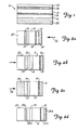
- Figure 1 is a diagrammatical view of a photosensor of the present invention.
- Figures 2A - 2D are diagrammatical views of X-ray sensors of the present invention.
- Figures 3A and 3B are diagrammatical views of alternative embodiments of X-rays sensors of the present invention.
- Figure 4 is a graphical view illustrating light and dark current characteristics of a photosensor of the present invention.
- Figure 5 is a graphical view illustrating quantum efficiency of a amorphous silicon sensor of the present invention.
- An amorphous silicon Schottky barrier photosensor of the present invention is generally illustrated at 10 in Figure 1.
- Like reference characters will be used to indicate like elements throughout the drawings.
- the photosensor 10 includes an undoped hydrogenated amorphous silicon layer (i-type a-Si:H) 12 and a n-type amorphous silicon layer 14 (n-type a-Si:H).
- the i-type a-Si:H layer and the n-type a-Si:H layer are disposed adjacent each other.
- a conductive metal layer 16 is disposed adjacent to the n-type a-Si:H layer on a side opposite from the i-type a-Si:H layer.
- a metal layer 18 is disposed adjacent side to the i-type a-Si:H layer on side opposite from the n-type a-Si:H layer.
- the layers 12, 14, 16, and 18 are typically disposed on a substrate 20.
- the conductive electrode layer 16 is deposited on the substrate 20.
- the substrate 20 can be made of Si02 coated silicon wafer, glass, polyimide, polyester, and stainless steel. A glass or quartz substrate is preferred.
- the conductive electrode layer 16 is deposited on the substrate preferably by sputtering. However, any other suitable process for applying a metal layer to a substrate is within the scope of the present invention.
- layer 16 serves as a conductive electrode. Suitable materials for use in layer 16 include tantalum, chromium, silver, aluminum, molybdenum, and titanium, with chromium and tantalum being preferred.
- a diffusion barrier layer may be deposited on the conductive layer to prevent migration of the silver and aluminum into the adjacent silicon layer.
- Diffusion barrier layer materials are known in the art and suitable materials are described by Tran et al. in "Effects of Carbon Profiles at the P/I Interface in Amorphous Silicon Solar Cells," Phys. State. Sol. (a) 99 , K13 (1987).
- a preferred diffusion barrier layer material is titanium nitride such as described by Jacobson et al. in "Amorphous Silicon P-I-N Layers Prepared by a Continuous Deposition Process or Polyimide Web," Proc. 19th IEEE Photovoltaic Specialists Conference 1987, p. 588.
- a transparent conductive oxide may be chosen as the material for the conductive layer 16.
- Typical TCO materials include indium tin oxide, tin oxide doped with fluorine or antimony, zinc oxide, and cadmium stannate.
- the conductive electrode layer 16 is deposited preferably by sputtering. However, any suitable process for forming such a layer on a substrate is within the scope of the present invention.
- the n-type a-Si:H amorphous silicon layer 14 in the arrangement illustrated in Figure 1 is deposited on the conductive layer 16.
- the i-type a-Si:H layer 12 is then deposited on the n-type a-Si:H layer 14.
- the i-type a-Si:H layer is preferably deposited at a thickness of approximately 200 to 1500 nm.
- the n-type a-Si:H amorphous silicon layer is preferably deposited at a thickness of approximately 20 to 100 nm. Both layers 12 and 14 are preferably deposited by a Plasma Enhanced Chemical Vapor Deposition (PECVD).
- PECVD Plasma Enhanced Chemical Vapor Deposition
- PECVD utilizes glow discharge deposition in an atmosphere that includes SiH4 and hydrogen in preferably a ratio of 1:9 at a total pressure of SiH4 and hydrogen of approximately 1 Torr.
- the temperature of the SiH4 substrate is in the range of 150°C to 350°C and preferably about 250°C.
- the n-type a-Si:H layer is formed by the addition of a dopant such as PH3 or AsH3 to the mixture of SiH4 and hydrogen in the ratio of about 1:100, also at a total pressure of approximately 1 Torr.
- the i-type A-Si:H layer can also be made of a silicon-based alloy such as silicon-germanium or silicon tin.
- plasma enhanced chemical vapor deposition systems may also be used such as electron cyclotron resonance chemical vapor deposition and photo-assisted chemical vapor deposition.
- other techniques such as sputtering, electron beam evaporation, or low pressure chemical vapor deposition may also be used to form the doped and undoped amorphous silicon layers.
- the metal layer 18 is then deposited on the i-type a-Si:H layer 12.
- Material used to form the layer 18 includes metals that may form silicides at low temperatures. Such metals include platinum, palladium, chromium, tungsten, and iron, with platinum being preferred.
- the layer 18 is preferably deposited by sputtering and is deposited to a thickness in the range of about 2 to 15 nm. After the layer 18 has been deposited, the layer 18 is subjected to an annealing process in a hydrogen atmosphere which is believed to reduce defect densities at the metal layer 18/a-Si:H layer 12 interface. Such a process reduces the dark current exhibited by the photosensor of the present invention by two to three orders of magnitude as compared to photosensors that have not been annealed.
- the annealing process of the present invention is carried out in a chamber that is evacuated to approximately 2 X 10 ⁇ 6 Torr. Hydrogen is introduced into the chamber at a slow flow rate backed up with a mechanical pump, to a total pressure between 0.2 and 1000 Torr to minimize the occurrence of contaminants in the chamber which can be critical to the success of the annealing process.
- an inert gas such as nitrogen, argon, xenon, krypton, or helium can be mixed with the hydrogen.
- inert gas is meant gas that under annealing conditions is not chemically reactive with other materials present in the chamber.
- the photosensor 10 is then heated to a temperature in the range of about 150°C to 350°C and preferably to a range between about 200°C to 300°C. The temperature is kept at the selected range for 10 to 60 minutes before being cooled down to room temperature.
- the hydrogen annealing can be carried out in plasma hydrogenation at a pressure of approximately 0.1 to 1.5 Torr and in a temperature range of approximately 150°C to 350°C for approximately 10 to 60 minutes. The temperature is thereafter brought back down to room temperature.
- the plasma hydrogenation can take place in the plasma-enhanced chemical vapor deposition system, electron cyclotron resonance chemical vapor deposition, or other plasma systems.
- An optional anti-reflection layer 22 may be deposited on to the layer 18 to a thickness in the range of 50 to 100 nm. Suitable materials for layer 22 include indium tin oxide (ITO), SnO2, ZnO, ZnS and Si3N4.
- the layers 16 and 18 may be reversed such that the metal layer is adjacent the substrate and the conductive layer 16 is on the opposite side of the amorphous silicon layers. If a transparent substrate is used and the activating light to which the device is subjected is incident on the substrate, then the layer 22 is made of a transparent conductive oxide and is placed between the layer 18 and the substrate 20.
- the process of the present invention produces a high quality amorphous silicon Schottky barrier photosensor.
- a quantum efficiency in the range of 20 percent to 50 percent is achieved without an anti-reflection coating.
- a quantum efficiency of 50 percent or higher is achieved under green light at a wave length of 545 nm over a wide range of intensities of up to 2.6 microwatts/cm2.
- quantum efficiency is meant the ratio of the number of collected charge carriers to the number of incident photons.
- Photosensors of the present invention exhibit dark currents of not more than 10 ⁇ 10A/cm2 at a temperature in the approximate range of 10°C and 30°C under an activation voltage of approximately -1V applied between the conductive layer and the metal layer and as low as 10 ⁇ 11A/cm2 as compared with 10 ⁇ 9A/cm2 for crystal silicon photosensors.
- the low dark current is surprising since the device before annealing has a very high dark current such as 10 ⁇ 7A/cm2.
- E-beam deposition provides metal layers which give dark currents that are lower than dark currents in layers which are produced using sputtering procedures. In addition, low dark currents can be achieved using simple vacuum annealing. However, E-beam deposition and simple vacuum annealing are not suitable techniques for producing photosensors in production quantities.
- thickness of the metal layer is important. For example, when platinum is used as the metal of choice, a thickness range of 100 to 150 A° is needed. Variation of the thickness will affect the performance of the device as a sensor.
- Sputtering is the preferred technique for forming a uniform layer over a large area, for example, several feet wide. The transport of material is made by the physical ejection of particles from the sputtering target by a momentum exchange rather than a chemical or thermal process. Using E-beam deposition, a uniform thickness is difficult to achieve even on an area that is 4 cm wide.
- the device 10 is particularly useful as a photo-electronic conversion device that is sensitive to X-rays for use as a photo-imaging element or a dosimeter in medical and industrial radiography.
- the device of the present invention has a high sensitivity to visible light and a very low dark current.
- the device of the present invention is useful in producing an X-ray sensor having a high signal-to-noise ratio in a two dimensional array of photo-electronic X-ray sensors when disposed on a flexible substrate.
- the X-ray sensor is producible in an integrated array of such sensors on the substrate.
- a luminescent layer is added to the photosensor described with reference to Figure 1.
- the addition of the luminescent layer provides the sensor with the capability of detecting X-rays.
- the luminescent layer is fluorescent and contains at least one X-ray phosphor.
- luminescent is meant both fluorescent and phosphorescent materials, with fluorescent being characterized as having negligible after-glow with such after-glow being pronounced in the phosphorescent material.
- the phosphors are chosen from those which emit visible light preferably in the wavelength range where a-Si:H photosensitive sensors are most sensitive, that is 400 nm to 700 nm. Enhancement of red sensitivity of the photosensor of the present invention can be accomplished by alloying the silicon with germanium, and enhancement of blue sensitivity can be achieved by alloying the silicon with carbon resulting from adding methane to the silane during the plasma enhanced chemical vapor deposition process.
- Suitable phosphors for use with the sensor of the present invention include gadolinium oxysulfide doped with terbium or with europium or samarium, yttrium oxide, calcium tungstate, and zinc sulfide.
- a preferred phosphor is gadolinium oxysulfide doped with terbium since the emitted wavelength of this phosphor matches the peak sensitivity of the photosensor of the present invention.
- the luminescent layers of the present invention are typically in the thickness range of about 300 to 200 microns.
- Figures 2A, 2B, 2C, and 2D illustrate various alternative arrangements of the sensor of the present invention including a luminescent layer containing one X-ray phosphor. In all cases, the layers are deposited as described with reference to Figure 1.
- the layers are arranged in the same order as in Figure 1, that is the metal layer 16 is adjacent to the substrate 20 with the n-type a-Si:H layer 14 adjacent the conductive layer 16.
- the i-type a-Si:H layer 12 is adjacent the n-type a-Si:H layer 14.
- the metal layer is deposited on the i-type a-Si:H layer 12 with the antireflection layer 22 deposited on the metal layer 18.
- a luminescent layer containing an X-ray phosphor is deposited on the antireflection layer so that the sensor detects X-rays incident from the general direction of arrow 26.
- the arrangement illustrated in Figure 2B includes the luminescent layer 24 being deposited directly on the substrate 20 with the layer 22 being deposited on the luminescent layer 24 and being made of a transparent conductive oxide.
- the n-type a-Si:H layer 14 is deposited on the layer 22 with the i-type a-Si:H layer l2 being deposited then on the n-type a-Si:H layer.
- the metal layer 18 is then deposited directly on the layer 12 with the conductive layer 16 being deposited on the metal layer 18.
- the substrate 20 is transparent to X-rays and the sensor detects X-rays incident on the substrate 20 from the general direction of arrow 28.
- the layers 22, 14, 12, 18, and 16 are in the same order as the arrangement of Figure 2B, except that the X-ray phosphor is now included in the substrate as a combined substrate and luminescent layer 30. X-rays are detected from the general direction of arrow 32, that is incident on the combined substrate and phosphor layer 30.
- the layer 22 performs as both an electrode and an anti-reflection layer.
- the embodiment illustrated in Figure 2D employs an arrangement that increases the optical efficiency of the luminescent layers.
- the n-type a-Si:H and i-type a-Si:H layers 14 and 12 are adjacent each other with the metal layer adjacent the i-type a-Si:H layer 12.
- layers 22A a TCO layer
- 22B an anti-reflection layer
- Adjacent both layers 22A and 22B on outer sides are luminescent layers 24A and 24B.
- the substrate is disposed adjacent the luminescent layer 24A.
- the embodiment of Figure 2D provides greater stopping power to X-rays while avoiding the optical inefficiency of excessive phosphor thickness of a single luminescent layer through the use of two luminescent layers.
- the phosphor can be a columnar structure phosphor.
- the columnar size of the phosphor is approximately equal to the pixel size of the array. Structured phosphors for radiographic imaging are discussed in European Patent Application 175,578 and in the Laboski et al. U.S. Patent 4,069,355. Columnar phosphor improves the quantum absorption of X-rays leading to improved signal-to-noise ratio, and improves the spatial resolution and sharpness of the image in the X-ray sensor.
- FIGS 3A and 3B Alternative embodiments 36 and 38 are illustrated in Figures 3A and 3B, respectively.
- the embodiments 36 and 38 include the common feature of a transparent glass substrate 40 with a luminescent layer 42 being disposed on one side and the photosensor of the present invention 44 being disposed on an opposite side of the glass substrate 40.
- the metal layer 18, i-type a-Si:H layer 12 and n-type a-Si:H layer 14 are in reverse order from those layers illustrated in the embodiment 38 of Figure 4B.
- the following examples are for illustrative purposes and are not to be considered as limiting the present invention.
- a photosensor of the general arrangement illustrated in Figure 1 was produced by initially depositing an approximately 1000 A° thick conductive tantalum metal electrode layer by sputtering on a SiO2 coated silicon wafer for use as the conductive layer. Next, using plasma enhanced chemical vapor deposition, an n-type hydrogenated amorphous silicon (n-type a-Si:H) of approximately 30 nm thickness was deposited as the ohmic contact on the tantalum metal layer. Next, an undoped hydrogenated amorphous silicon (i-type a-Si:H) layer was deposited by plasma enhanced chemical vapor deposition on the n-type a-Si:H layer of approximately 500 nm thickness.
- n-type a-Si:H n-type hydrogenated amorphous silicon
- n-type and i-type a-Si:H layers were formed utilizing a capacitively coupled reactor which consisted of two 5-inch by 5-inch parallel plate electrodes placed approximately 3/4 inch apart. The discharge was excited by a 13.56 MHz RF generator and the system was equipped with a turbomolecular pump which was backed by a mechanical pump. A source gas was fed into the reactor through a bottom RF driven electrode which had multiple holes based on the "shower head" concept. Both amorphous silicon layers were prepared at an RF power of 6-10W.
- Both amorphous silicon layers were produced in sequence in an atmosphere of SiH4 and hydrogen at a ratio of 1:9, at a total pressure of approximately 1 Torr, and with the glass substrate temperature being approximately 250°C.
- the n-type a-Si:H layer was formed with the addition of PH3 to the gas mixture in the ratio of 1:100 at a total pressure of 1 Torr.
- the chamber was pumped with a turbomolecular pump for 30 minutes before the deposition of the i-type a-Si:H layer.
- a layer of platinum metal was sputtered on to the i-type a-Si:H layer to a thickness of approximately 10 nm.
- the platinum was then annealed under the following conditions.
- the chamber was evacuated to 2 X 10 ⁇ 6 Torr.
- Hydrogen was introduced into the chamber at a flow rate of 5 sccm to a total pressure of 1 Torr.
- the photosensor was then heated to approximately 200°C and maintained at this temperature for approximately 30 minutes before being cooled down to room temperature.
- Hydrogen was introduced into the chamber in a dynamic mode to avoid contamination, that is hydrogen flow backed-up with a mechanical pump.
- ITO indium tin oxide
- the photosensor produced was a high quality amorphous silicon Schottky barrier photosensor which when activated with a voltage of -1V applied between the platinum layer and the tantalum metal electrode layer achieved the quantum efficiency of 25 percent without anti-reflection coating, and 50 percent with an anti-reflection coating under green light of a wavelength of approximately 545 nm at an intensity of 2.6 microwatts/cm2.
- Current-voltage characteristics of the amorphous silicon Schottky barrier sensor are illustrated in Figure 4.
- a dark current as low as 10 ⁇ 11 A/cm2 at -1V and a photo current of 10 ⁇ 6 A/cm2 was achieved at 2.6 microwatts/cm2.
- a quantum efficiency as high as 45 percent at 545 nm without an anti-reflection layer was demonstrated, as illustrated in Figure 5.
- An X-ray sensitive device was constructed using the photosensor of Example 1 by coating a phosphor layer of gadolinium oxysulfide doped with terbium approximately 70 microns thick on the ITO layer.
- the gadolinium oxysulfide doped with terbium layer was obtained by a sedimentation technique from a suspension of phosphor powder in a binder as follows: 7 grams of phosphor were dispersed in 10 grams of polymethylmethacrylate with 10 grams of butylacrylate, 10 grams of methylisobutylketone, and 10 grams of ethylacetate. The above gave a dispersion having a grain size and size distribution that is typical of a commercially available X-ray phosphor marketed by 3M Company of St. Paul, Minnesota, under the trademark T6 TRIMAX.
- the X-ray sensor of this example was measured at 90 KVp, 200 msec and a dynamic range of between 103 to 104 was achieved. These results indicate that the device is adequate for an X-ray sensor.
Landscapes
- Light Receiving Elements (AREA)
- Solid State Image Pick-Up Elements (AREA)
Abstract
Description
- The present invention relates to amorphous silicon sensors, and in particular, it relates to an amorphous silicon Schottky barrier device having a metal annealed layer.
- A semiconductor X-ray sensor is a device for converting X-ray energy to an electrical signal. In general, such sensors sense either the collection of the charge generated by absorption of the incident X-ray photons in the semiconductor itself or the collection of the charge generated in the semiconductor by absorption of visible light photons which are produced by a phosphor or scintillation element excited by the X-rays.
- The absorption and conversion of X-rays into light photons by a phosphor screen followed by the conversion of the light photons into electrical charge in the semiconductor device is the more efficient process and is generally chosen whenever the statistical accuracy of the number of photons is preferred to the accuracy in the energy or time resolution of the impinging radiation. This approach is suited for Computer Tomography and Electronic Radiography where the image is close to the quantum limit because of the very low dosage requirement.
- Beerlage et al in an article entitled "Digital Slot Radiography Based on a Linear X-Ray Image Intensifier and Two-Dimensional Image Sensors" describe the use of digital radiography. Digital radiography is useful in situations where a large area needs to be imaged. However, the sensors used in digital radiography are expensive hybrid assemblies of discrete single crystal devices and do not allow high resolution and high quality imaging.
- A phosphor layer coated on metal electrodes of a junction field effect transistor (JFET) that is deposited on top of amorphous silicon Schottky devices as described in European Patent Application 189,710. A charge is injected and trapped through the source and drain electrodes into the potential well close to the gate electrode. This charge inhibits the conduction between the source and drain electrodes and can be neutralized by charge generation produced by the light from the phosphorus screen. Current between the source and drain electrodes is taken as the signal. In European Patent Application 163,956, an X-ray sensor having an amorphous silicon p-i-n structure is described. The sensor structure is conventional and utilizes single transistors or single diodes as blocking elements in a pixel.
- More recently an amorphous silicon X-ray sensor has been described in Japanese laid-open patent applications Nos. 61-196582, 61-196572, 61-196571, and 61-196570. The amorphous silicon X-ray sensor described in these Japanese patent applications is fabricated on glass substrates by the decomposition of SiH₄/H₂ mixtures containing the desired amounts of CH₄, B₂H₆, PH₃ in a RF glow discharge deposition system to produce amorphous silicon layers (a-Si:H) with various levels of doping. The structure of the sensor is a glass substrate /ITO (Indium Tin Oxide) layer /p-type a-SiC:H layer /i-type a-Si:H layer /microcrystalline n-type a-Si:H layer /Al layer. The thickness of the p-type and n-type layers is 120-150 Angstrom and 500 Angstrom, respectively. A layer of ZnS (Ni doped) or CaWO4 phosphor is coated on the front surface of the glass substrate. When X-rays are incident on the phosphor, green or blue light is emitted. The light then penetrates the glass substrate and finally enters the p-i-n sensor. However, systems made from this sensor suffer from image contrast losses and are limited in spatial resolution and dynamic range.
- Amorphous silicon Schottky barrier diodes and photosensors are well known in the art. Solar cells made using amorphous silicon (a-Si) produced by RF glow discharge in silane were found to contain a much smaller density of defects than samples previously made by direct evaporation or sputtering (D. E. Carlson and C. R. Wronski, "Amorphous Silicon Solar Cell", App. Phys. Lett. Vol. 28, 671 (1976)). Electrical properties of Schottky barriers formed between undoped amorphous silicon and metals such as chromium, palladium, rhodium, and platinum have been studied (C. R. Wronski and D. E. Carlson, "Surface States and Barrier Heights of Metal-Amorphous Silicon Schottky Barriers", Solid State Comm. Vol. 23, 421 (1977)).
- Schottky diodes formed between platinum and undoped a-Si:H produced by RF glow discharge in silane/hydrogen mixtures, are shown (A. Deneuville and M. H. Brodsky, "Influence of Preparation Conditions on Forward-Bias Currents of Amorphous Silicon Schottky Diodes", J. Appl. Phys. Vol. 50, 1414 (1979)) to have improved characteristics (closer to ideality) on post deposition annealing at a temperature equal to the deposition temperature. No details of the atmosphere are given explicitly. The formation of metal silicide at the metal/a-Si:H interfaces on post-deposition annealing is studied in M. J. Thompson et al, "Silicide Formation in Pd-a-Si:H Schottky Barriers", Appl. Phys. Lett. Vol. 39, 274 (1981). Annealing was under vacuum at 180°C for 15 min. Ideality factors improved and became stable on annealing.
- In R. J. Nemanich et al, "Initial Reactions at the Interface of Pt and Amorphous Silicon", J. Vac. Sci. detailed studies were described of the Pt silicide layers formed between a thin electron beam deposited Pt layer and a-Si:H layer in a Schottky barrier diode. No photo response characteristics were examined but the backward bias (-1V) current densities were given as about 10⁻¹⁰A./cm² as-formed and 10⁻¹¹A./cm² after vacuum annealing at about 200°C.
- In R. J. Nemanich in "Semiconductors and Semimetals", Vol. 21, Part C, page 376, edited by Jacques Pankove, Academic Press 1984, metal silicides are reported to occur at junctions with a-Si:H with the following metals, chromium, nickel, palladium, and platinum.
- The present invention includes a photosensor exhibiting low dark current and a high sensitivity to visible light. The sensor includes a doped hydrogenated amorphous silicon layer adjacent an undoped hydrogenated amorphous silicon layer with the two layers sandwiched by a conductive layer on one side and a metal layer having been annealed in a hydrogen atmosphere.
- In a preferred embodiment, the photosensor of the present invention is useful as photo-electronic conversion device that is sensitive to X-rays. The photosensor is attached to a substrate and a luminescent layer containing at least one x-ray phosphor is added to the photosensor.
- Figure 1 is a diagrammatical view of a photosensor of the present invention.
- Figures 2A - 2D are diagrammatical views of X-ray sensors of the present invention.
- Figures 3A and 3B are diagrammatical views of alternative embodiments of X-rays sensors of the present invention.
- Figure 4 is a graphical view illustrating light and dark current characteristics of a photosensor of the present invention.
- Figure 5 is a graphical view illustrating quantum efficiency of a amorphous silicon sensor of the present invention.
- An amorphous silicon Schottky barrier photosensor of the present invention is generally illustrated at 10 in Figure 1. Like reference characters will be used to indicate like elements throughout the drawings.
- The
photosensor 10 includes an undoped hydrogenated amorphous silicon layer (i-type a-Si:H) 12 and a n-type amorphous silicon layer 14 (n-type a-Si:H). The i-type a-Si:H layer and the n-type a-Si:H layer are disposed adjacent each other. Aconductive metal layer 16 is disposed adjacent to the n-type a-Si:H layer on a side opposite from the i-type a-Si:H layer. Ametal layer 18 is disposed adjacent side to the i-type a-Si:H layer on side opposite from the n-type a-Si:H layer. Thelayers substrate 20. - In the embodiment illustrated in Figure 1, initially the
conductive electrode layer 16 is deposited on thesubstrate 20. Thesubstrate 20 can be made of Si0₂ coated silicon wafer, glass, polyimide, polyester, and stainless steel. A glass or quartz substrate is preferred. Theconductive electrode layer 16 is deposited on the substrate preferably by sputtering. However, any other suitable process for applying a metal layer to a substrate is within the scope of the present invention. - The primary purpose of
layer 16 is to serve as a conductive electrode. Suitable materials for use inlayer 16 include tantalum, chromium, silver, aluminum, molybdenum, and titanium, with chromium and tantalum being preferred. - If silver and aluminum are used as metals to form the
conductive layer 16, a diffusion barrier layer may be deposited on the conductive layer to prevent migration of the silver and aluminum into the adjacent silicon layer. Diffusion barrier layer materials are known in the art and suitable materials are described by Tran et al. in "Effects of Carbon Profiles at the P/I Interface in Amorphous Silicon Solar Cells," Phys. State. Sol. (a) 99, K13 (1987). A preferred diffusion barrier layer material is titanium nitride such as described by Jacobson et al. in "Amorphous Silicon P-I-N Layers Prepared by a Continuous Deposition Process or Polyimide Web," Proc. 19th IEEE Photovoltaic Specialists Conference 1987, p. 588. - If
layer 16 is to serve as a transparent conductive layer, then a transparent conductive oxide (TCO) may be chosen as the material for theconductive layer 16. Typical TCO materials that are well known in the art include indium tin oxide, tin oxide doped with fluorine or antimony, zinc oxide, and cadmium stannate. - The
conductive electrode layer 16 is deposited preferably by sputtering. However, any suitable process for forming such a layer on a substrate is within the scope of the present invention. - The n-type a-Si:H
amorphous silicon layer 14 in the arrangement illustrated in Figure 1 is deposited on theconductive layer 16. The i-type a-Si:H layer 12 is then deposited on the n-type a-Si:H layer 14. The i-type a-Si:H layer is preferably deposited at a thickness of approximately 200 to 1500 nm. The n-type a-Si:H amorphous silicon layer is preferably deposited at a thickness of approximately 20 to 100 nm. Both layers 12 and 14 are preferably deposited by a Plasma Enhanced Chemical Vapor Deposition (PECVD). PECVD utilizes glow discharge deposition in an atmosphere that includes SiH₄ and hydrogen in preferably a ratio of 1:9 at a total pressure of SiH₄ and hydrogen of approximately 1 Torr. The temperature of the SiH₄ substrate is in the range of 150°C to 350°C and preferably about 250°C. The n-type a-Si:H layer is formed by the addition of a dopant such as PH₃ or AsH₃ to the mixture of SiH₄ and hydrogen in the ratio of about 1:100, also at a total pressure of approximately 1 Torr. - The i-type A-Si:H layer can also be made of a silicon-based alloy such as silicon-germanium or silicon tin.
- Other plasma enhanced chemical vapor deposition systems may also be used such as electron cyclotron resonance chemical vapor deposition and photo-assisted chemical vapor deposition. In addition, other techniques such as sputtering, electron beam evaporation, or low pressure chemical vapor deposition may also be used to form the doped and undoped amorphous silicon layers.
- The
metal layer 18 is then deposited on the i-type a-Si:H layer 12. Material used to form thelayer 18 includes metals that may form silicides at low temperatures. Such metals include platinum, palladium, chromium, tungsten, and iron, with platinum being preferred. - The
layer 18 is preferably deposited by sputtering and is deposited to a thickness in the range of about 2 to 15 nm. After thelayer 18 has been deposited, thelayer 18 is subjected to an annealing process in a hydrogen atmosphere which is believed to reduce defect densities at themetal layer 18/a-Si:H layer 12 interface. Such a process reduces the dark current exhibited by the photosensor of the present invention by two to three orders of magnitude as compared to photosensors that have not been annealed. - The annealing process of the present invention is carried out in a chamber that is evacuated to approximately 2
X 10⁻⁶ Torr. Hydrogen is introduced into the chamber at a slow flow rate backed up with a mechanical pump, to a total pressure between 0.2 and 1000 Torr to minimize the occurrence of contaminants in the chamber which can be critical to the success of the annealing process. Optionally, an inert gas such as nitrogen, argon, xenon, krypton, or helium can be mixed with the hydrogen. By inert gas is meant gas that under annealing conditions is not chemically reactive with other materials present in the chamber. Thephotosensor 10 is then heated to a temperature in the range of about 150°C to 350°C and preferably to a range between about 200°C to 300°C. The temperature is kept at the selected range for 10 to 60 minutes before being cooled down to room temperature. - Alternatively, the hydrogen annealing can be carried out in plasma hydrogenation at a pressure of approximately 0.1 to 1.5 Torr and in a temperature range of approximately 150°C to 350°C for approximately 10 to 60 minutes. The temperature is thereafter brought back down to room temperature. The plasma hydrogenation can take place in the plasma-enhanced chemical vapor deposition system, electron cyclotron resonance chemical vapor deposition, or other plasma systems.
- An
optional anti-reflection layer 22 may be deposited on to thelayer 18 to a thickness in the range of 50 to 100 nm. Suitable materials forlayer 22 include indium tin oxide (ITO), SnO₂, ZnO, ZnS and Si₃N₄. - The
layers conductive layer 16 is on the opposite side of the amorphous silicon layers. If a transparent substrate is used and the activating light to which the device is subjected is incident on the substrate, then thelayer 22 is made of a transparent conductive oxide and is placed between thelayer 18 and thesubstrate 20. - The process of the present invention produces a high quality amorphous silicon Schottky barrier photosensor. When activated, with a voltage of -1V applied between the
conductive layer 16 and themetal layer 18, a quantum efficiency in the range of 20 percent to 50 percent is achieved without an anti-reflection coating. With an anti-reflection coating, a quantum efficiency of 50 percent or higher is achieved under green light at a wave length of 545 nm over a wide range of intensities of up to 2.6 microwatts/cm². By quantum efficiency is meant the ratio of the number of collected charge carriers to the number of incident photons. - Photosensors of the present invention exhibit dark currents of not more than 10⁻¹⁰A/cm² at a temperature in the approximate range of 10°C and 30°C under an activation voltage of approximately -1V applied between the conductive layer and the metal layer and as low as 10⁻¹¹A/cm² as compared with 10⁻⁹A/cm² for crystal silicon photosensors. The low dark current is surprising since the device before annealing has a very high dark current such as 10⁻⁷A/cm².
- Other deposition methods such as E-beam deposition provide metal layers which give dark currents that are lower than dark currents in layers which are produced using sputtering procedures. In addition, low dark currents can be achieved using simple vacuum annealing. However, E-beam deposition and simple vacuum annealing are not suitable techniques for producing photosensors in production quantities. In the devices of the present invention, thickness of the metal layer is important. For example, when platinum is used as the metal of choice, a thickness range of 100 to 150 A° is needed. Variation of the thickness will affect the performance of the device as a sensor. Sputtering is the preferred technique for forming a uniform layer over a large area, for example, several feet wide. The transport of material is made by the physical ejection of particles from the sputtering target by a momentum exchange rather than a chemical or thermal process. Using E-beam deposition, a uniform thickness is difficult to achieve even on an area that is 4 cm wide.
- Dark currents of photosensors annealed under different atmospheres such as hydrogen, argon, and simple vacuum annealing were measured. Results indicated that annealing in a hydrogen atmosphere gave the best results. The dark current of the photosensor annealed in the hydrogen atmosphere of the present invention was more than one order of magnitude lower than the dark current of photosensors annealed under argon or simple vacuum annealing.
- The
device 10 is particularly useful as a photo-electronic conversion device that is sensitive to X-rays for use as a photo-imaging element or a dosimeter in medical and industrial radiography. The device of the present invention has a high sensitivity to visible light and a very low dark current. The device of the present invention is useful in producing an X-ray sensor having a high signal-to-noise ratio in a two dimensional array of photo-electronic X-ray sensors when disposed on a flexible substrate. The X-ray sensor is producible in an integrated array of such sensors on the substrate. - For use as an X-ray sensor, a luminescent layer is added to the photosensor described with reference to Figure 1. The addition of the luminescent layer provides the sensor with the capability of detecting X-rays. Preferably, the luminescent layer is fluorescent and contains at least one X-ray phosphor. By luminescent is meant both fluorescent and phosphorescent materials, with fluorescent being characterized as having negligible after-glow with such after-glow being pronounced in the phosphorescent material.
- The phosphors are chosen from those which emit visible light preferably in the wavelength range where a-Si:H photosensitive sensors are most sensitive, that is 400 nm to 700 nm. Enhancement of red sensitivity of the photosensor of the present invention can be accomplished by alloying the silicon with germanium, and enhancement of blue sensitivity can be achieved by alloying the silicon with carbon resulting from adding methane to the silane during the plasma enhanced chemical vapor deposition process.
- Examples of suitable phosphors for use with the sensor of the present invention include gadolinium oxysulfide doped with terbium or with europium or samarium, yttrium oxide, calcium tungstate, and zinc sulfide. A preferred phosphor is gadolinium oxysulfide doped with terbium since the emitted wavelength of this phosphor matches the peak sensitivity of the photosensor of the present invention. The luminescent layers of the present invention are typically in the thickness range of about 300 to 200 microns.
- Figures 2A, 2B, 2C, and 2D illustrate various alternative arrangements of the sensor of the present invention including a luminescent layer containing one X-ray phosphor. In all cases, the layers are deposited as described with reference to Figure 1.
- In the arrangement illustrated in Figure 2A, the layers are arranged in the same order as in Figure 1, that is the
metal layer 16 is adjacent to thesubstrate 20 with the n-type a-Si:H layer 14 adjacent theconductive layer 16. The i-type a-Si:H layer 12 is adjacent the n-type a-Si:H layer 14. The metal layer is deposited on the i-type a-Si:H layer 12 with theantireflection layer 22 deposited on themetal layer 18. A luminescent layer containing an X-ray phosphor is deposited on the antireflection layer so that the sensor detects X-rays incident from the general direction ofarrow 26. - The arrangement illustrated in Figure 2B includes the
luminescent layer 24 being deposited directly on thesubstrate 20 with thelayer 22 being deposited on theluminescent layer 24 and being made of a transparent conductive oxide. The n-type a-Si:H layer 14 is deposited on thelayer 22 with the i-type a-Si:H layer l2 being deposited then on the n-type a-Si:H layer. Themetal layer 18 is then deposited directly on thelayer 12 with theconductive layer 16 being deposited on themetal layer 18. In the arrangement of Figure 2B, thesubstrate 20 is transparent to X-rays and the sensor detects X-rays incident on thesubstrate 20 from the general direction of arrow 28. - In the arrangement of Figure 2C, the
layers luminescent layer 30. X-rays are detected from the general direction of arrow 32, that is incident on the combined substrate andphosphor layer 30. - With respect to the arrangements illustrated in Figures 2B and 2C, the
layer 22 performs as both an electrode and an anti-reflection layer. - The embodiment illustrated in Figure 2D, employs an arrangement that increases the optical efficiency of the luminescent layers. The n-type a-Si:H and i-type a-Si:H layers 14 and 12 are adjacent each other with the metal layer adjacent the i-type a-Si:
H layer 12. On opposing sides of the combined layers 14, 12, and 18, are included layers 22A (a TCO layer) and 22B ( an anti-reflection layer). Adjacent both layers 22A and 22B on outer sides are luminescent layers 24A and 24B. The substrate is disposed adjacent the luminescent layer 24A. The embodiment of Figure 2D provides greater stopping power to X-rays while avoiding the optical inefficiency of excessive phosphor thickness of a single luminescent layer through the use of two luminescent layers. - Other methods of increasing the optical efficiency of luminescent layers are includable in the present invention. These include the use of back reflecting layers which prevent escape of emitted light from a surface of the phosphor layer facing away from the photodetector. The phosphor can be a columnar structure phosphor. When the X-ray device of the present invention is used in a two-dimensional array, preferably, the columnar size of the phosphor is approximately equal to the pixel size of the array. Structured phosphors for radiographic imaging are discussed in European Patent Application 175,578 and in the Laboski et al. U.S. Patent 4,069,355. Columnar phosphor improves the quantum absorption of X-rays leading to improved signal-to-noise ratio, and improves the spatial resolution and sharpness of the image in the X-ray sensor.
-
Alternative embodiments embodiments transparent glass substrate 40 with aluminescent layer 42 being disposed on one side and the photosensor of thepresent invention 44 being disposed on an opposite side of theglass substrate 40. In theembodiment 36, themetal layer 18, i-type a-Si:H layer 12 and n-type a-Si:H layer 14 are in reverse order from those layers illustrated in theembodiment 38 of Figure 4B. The following examples are for illustrative purposes and are not to be considered as limiting the present invention. - A photosensor of the general arrangement illustrated in Figure 1 was produced by initially depositing an approximately 1000 A° thick conductive tantalum metal electrode layer by sputtering on a SiO₂ coated silicon wafer for use as the conductive layer. Next, using plasma enhanced chemical vapor deposition, an n-type hydrogenated amorphous silicon (n-type a-Si:H) of approximately 30 nm thickness was deposited as the ohmic contact on the tantalum metal layer. Next, an undoped hydrogenated amorphous silicon (i-type a-Si:H) layer was deposited by plasma enhanced chemical vapor deposition on the n-type a-Si:H layer of approximately 500 nm thickness. The deposition of both the n-type and i-type a-Si:H layers was performed utilizing a capacitively coupled reactor which consisted of two 5-inch by 5-inch parallel plate electrodes placed approximately 3/4 inch apart. The discharge was excited by a 13.56 MHz RF generator and the system was equipped with a turbomolecular pump which was backed by a mechanical pump. A source gas was fed into the reactor through a bottom RF driven electrode which had multiple holes based on the "shower head" concept. Both amorphous silicon layers were prepared at an RF power of 6-10W. Both amorphous silicon layers were produced in sequence in an atmosphere of SiH₄ and hydrogen at a ratio of 1:9, at a total pressure of approximately 1 Torr, and with the glass substrate temperature being approximately 250°C. The n-type a-Si:H layer was formed with the addition of PH₃ to the gas mixture in the ratio of 1:100 at a total pressure of 1 Torr.
- In order to eliminate cross contamination of phosphorus carried over from the deposition of the n-type a-Si:H to the i-type a-Si:H layer, the chamber was pumped with a turbomolecular pump for 30 minutes before the deposition of the i-type a-Si:H layer.
- Next, a layer of platinum metal was sputtered on to the i-type a-Si:H layer to a thickness of approximately 10 nm. The platinum was then annealed under the following conditions. The chamber was evacuated to 2
X 10⁻⁶ Torr. Hydrogen was introduced into the chamber at a flow rate of 5 sccm to a total pressure of 1 Torr. The photosensor was then heated to approximately 200°C and maintained at this temperature for approximately 30 minutes before being cooled down to room temperature. Hydrogen was introduced into the chamber in a dynamic mode to avoid contamination, that is hydrogen flow backed-up with a mechanical pump. - Next, an anti-reflection layer of indium tin oxide (ITO) was then deposited on to the platinum layer to a thickness of approximately 70 nm.
- The photosensor produced was a high quality amorphous silicon Schottky barrier photosensor which when activated with a voltage of -1V applied between the platinum layer and the tantalum metal electrode layer achieved the quantum efficiency of 25 percent without anti-reflection coating, and 50 percent with an anti-reflection coating under green light of a wavelength of approximately 545 nm at an intensity of 2.6 microwatts/cm². Current-voltage characteristics of the amorphous silicon Schottky barrier sensor are illustrated in Figure 4. A dark current as low as 10⁻¹¹ A/cm² at -1V and a photo current of 10⁻⁶ A/cm² was achieved at 2.6 microwatts/cm². A quantum efficiency as high as 45 percent at 545 nm without an anti-reflection layer was demonstrated, as illustrated in Figure 5.
- Major optical and electrical properties of the i-type a-Si:H layer are as follows:
- 1. Optical band gap of 1.75 eV.
- 2. ESR spin density of 10¹⁵ cm⁻³.
- 3. IR absorption peaks at 2000 cm⁻¹ and 630 cm⁻¹.
- 4. Photo to dark conductively ratio of 10⁵ (AM1)
- The above readings indicate a high quality amorphous silicon device.
- An X-ray sensitive device was constructed using the photosensor of Example 1 by coating a phosphor layer of gadolinium oxysulfide doped with terbium approximately 70 microns thick on the ITO layer. The gadolinium oxysulfide doped with terbium layer was obtained by a sedimentation technique from a suspension of phosphor powder in a binder as follows: 7 grams of phosphor were dispersed in 10 grams of polymethylmethacrylate with 10 grams of butylacrylate, 10 grams of methylisobutylketone, and 10 grams of ethylacetate. The above gave a dispersion having a grain size and size distribution that is typical of a commercially available X-ray phosphor marketed by 3M Company of St. Paul, Minnesota, under the trademark T6 TRIMAX.
- The X-ray sensor of this example was measured at 90 KVp, 200 msec and a dynamic range of between 10³ to 10⁴ was achieved. These results indicate that the device is adequate for an X-ray sensor.
- Although the present invention has been described with reference to preferred embodiments, workers skilled in the art will recognize that changes may be made in form and detail without departing from the spirit and scope of the invention.
Claims (11)
- A sensor device comprising:
an amorphous silicon Schottky barrier diode having a metal layer annealed in a hydrogen atmosphere. - The sensor device of claim 1 wherein the diode comprises:
a conductive layer;
a doped hydrogenated amorphous silicon layer;
an undoped hydrogenated amorphous silicon layer adjacent the doped hydrogenated amorphous silicon layer;
the metal layer annealed by the hydrogen atmosphere; and
wherein the doped and undoped hydrogenated amorphous silicon layers are disposed between the metal layer and the conductive layer. - A process for making the sensor device of claim 2, the process comprising:
initially depositing on the substrate, the electrode layer, the doped hydrogenated amorphous silicon layer, the undoped hydrogenated amorphous silicon layer adjacent the doped hydrogenated amorphous silicon layer, and the metal layer; and
subsequently annealing the sensor in a hydrogen atmosphere. - The device of claim 1 and further including an illuminescent layer disposed on the Schottky barrier diode, the illuminescent layer having an X-ray sensitive phosphor.
- The device of claim 1 wherein the device exhibits dark currents of not more than approximately 10⁻ ¹⁰ A/cm² at a temperature in the approximate range of 10°C to 30°C under an activation voltage of approximately -1V applied between conductive layers of the diode.
- The device of claim 2 and further including an anti-reflection layer adjacent the metal layer.
- The device of claim 6 and further including a luminescent layer disposed adjacent the anti-reflection layer.
- The device of claim 2 and further including a luminescent layer disposed adjacent the conductive layer.
- The device of claim 2 and further including a substrate disposed adjacent the conductive layer, the substrate including an X-ray phosphor compound disposed therein.
- The device of claim 2 and further including a transparent conductive oxide layer disposed adjacent the metal layer, and a first luminescent layer disposed adjacent the conductive layer and a second luminescent layer disposed adjacent the transparent conductive oxide layer.
- The device of claim 2 and further including a glass substrate disposed adjacent the conductive layer and a luminescent layer disposed on the glass substrate on a side opposite from the conductive layer.
Applications Claiming Priority (2)
| Application Number | Priority Date | Filing Date | Title |
|---|---|---|---|
| US45828889A | 1989-12-28 | 1989-12-28 | |
| US458288 | 1989-12-28 |
Publications (2)
| Publication Number | Publication Date |
|---|---|
| EP0438889A1 true EP0438889A1 (en) | 1991-07-31 |
| EP0438889B1 EP0438889B1 (en) | 1997-09-17 |
Family
ID=23820182
Family Applications (1)
| Application Number | Title | Priority Date | Filing Date |
|---|---|---|---|
| EP90313630A Expired - Lifetime EP0438889B1 (en) | 1989-12-28 | 1990-12-14 | Method of forming an amorphous silicon sensor |
Country Status (7)
| Country | Link |
|---|---|
| US (1) | US5291036A (en) |
| EP (1) | EP0438889B1 (en) |
| JP (1) | JPH04251988A (en) |
| KR (1) | KR910013595A (en) |
| CA (1) | CA2031628A1 (en) |
| DE (1) | DE69031459T2 (en) |
| IL (1) | IL96561A0 (en) |
Cited By (4)
| Publication number | Priority date | Publication date | Assignee | Title |
|---|---|---|---|---|
| EP0526817A1 (en) * | 1991-08-05 | 1993-02-10 | Siemens Aktiengesellschaft | Radiation detector |
| WO2002071497A1 (en) * | 2001-03-01 | 2002-09-12 | Stmicroelectronics Nv | Opto-electronic component |
| CN100437221C (en) * | 2005-10-14 | 2008-11-26 | 群康科技(深圳)有限公司 | Liquid crystal displaying device and mfg. method thereof |
| EP2058751A2 (en) | 2007-11-08 | 2009-05-13 | Robert Bosch GmbH | Camera for recording the surroundings of a vehicle |
Families Citing this family (13)
| Publication number | Priority date | Publication date | Assignee | Title |
|---|---|---|---|---|
| US5449923A (en) * | 1992-03-31 | 1995-09-12 | Industrial Technology Research Institute | Amorphous silicon color detector |
| US5556716A (en) * | 1994-08-25 | 1996-09-17 | E. I. Du Pont De Nemours And Company | X-ray photoconductive compositions for x-ray radiography |
| KR100214267B1 (en) * | 1995-04-07 | 1999-08-02 | 김영환 | Semiconductor device fabrication method |
| US5989652A (en) * | 1997-01-31 | 1999-11-23 | Tokyo Electron Limited | Method of low temperature plasma enhanced chemical vapor deposition of tin film over titanium for use in via level applications |
| US6057587A (en) * | 1997-08-28 | 2000-05-02 | Vlsi Technology, Inc. | Semiconductor device with anti-reflective structure |
| US7671342B2 (en) * | 2005-01-11 | 2010-03-02 | Siemens Medical Solutions Usa, Inc. | Multi-layer detector and method for imaging |
| DE102005019259A1 (en) * | 2005-04-26 | 2006-11-09 | Giesecke & Devrient Gmbh | Device for examining documents |
| CN100461435C (en) * | 2006-09-11 | 2009-02-11 | 中国科学院上海技术物理研究所 | Anti-reflective film and preparation method of very long-wave mercury cadmium telluride infrared focal plane detector |
| US7482646B2 (en) * | 2006-10-18 | 2009-01-27 | Hejian Technology (Suzhou) Co., Ltd. | Image sensor |
| KR100998618B1 (en) * | 2007-06-29 | 2010-12-07 | (주)넥센나노텍 | Cathode active material for silicon-based lithium secondary battery mixed with carbon nanofibers |
| KR20120042301A (en) * | 2010-10-25 | 2012-05-03 | 삼성전자주식회사 | Method of fabricating semiconductor device |
| CN104334767B (en) | 2012-03-05 | 2017-06-09 | 第一太阳能有限公司 | Method and apparatus for forming transparent conductive oxides using hydrogen |
| TWI545788B (en) | 2014-10-03 | 2016-08-11 | 財團法人工業技術研究院 | Sheet and module structure |
Citations (2)
| Publication number | Priority date | Publication date | Assignee | Title |
|---|---|---|---|---|
| US4096387A (en) * | 1976-12-09 | 1978-06-20 | Rca Corporation | Ultraviolet radiation detector |
| US4811069A (en) * | 1987-02-23 | 1989-03-07 | Oki Electric Industry Co., Ltd. | Photoelectric conversion device |
Family Cites Families (18)
| Publication number | Priority date | Publication date | Assignee | Title |
|---|---|---|---|---|
| US4011454A (en) * | 1975-04-28 | 1977-03-08 | General Electric Company | Structured X-ray phosphor screen |
| US4064521A (en) * | 1975-07-28 | 1977-12-20 | Rca Corporation | Semiconductor device having a body of amorphous silicon |
| US4200473A (en) * | 1979-03-12 | 1980-04-29 | Rca Corporation | Amorphous silicon Schottky barrier solar cells incorporating a thin insulating layer and a thin doped layer |
| EP0309000B1 (en) * | 1981-07-17 | 1992-10-14 | Kanegafuchi Kagaku Kogyo Kabushiki Kaisha | Amorphous semiconductor and amorphous silicon photovoltaic device |
| FR2523371A1 (en) * | 1982-03-10 | 1983-09-16 | Contellec Michel Le | HYDROGEN AMORPHOUS SILICON CARBIDE PHOTOCONDUCTIVE ELEMENT AND VIDEO RETINE CELL USING SUCH AN ELEMENT |
| US4607164A (en) * | 1982-07-28 | 1986-08-19 | Hitachi, Ltd. | Radiation detecting apparatus |
| JPS59110179A (en) * | 1982-12-16 | 1984-06-26 | Hitachi Ltd | Semiconductor device and manufacture thereof |
| JPS60230132A (en) * | 1984-04-27 | 1985-11-15 | Fuji Photo Film Co Ltd | Reader for radiation image information |
| US4672454A (en) * | 1984-05-04 | 1987-06-09 | Energy Conversion Devices, Inc. | X-ray image scanner and method |
| EP0163956A3 (en) * | 1984-05-04 | 1988-04-06 | Energy Conversion Devices, Inc. | Intergrated radiation sensing array |
| US4660095A (en) * | 1984-05-04 | 1987-04-21 | Energy Conversion Devices, Inc. | Contact-type document scanner and method |
| FR2575602B1 (en) * | 1984-12-27 | 1987-01-30 | Thomson Csf | LARGE FORMAT PHOTOSENSITIVE DEVICE AND METHOD OF USE |
| JPS61196572A (en) * | 1985-02-25 | 1986-08-30 | Hitachi Zosen Corp | Amorphous silicon x-ray sensor |
| JPS61196571A (en) * | 1985-02-25 | 1986-08-30 | Hitachi Zosen Corp | Amorphous silicon x-ray sensor |
| JPS61196570A (en) * | 1985-02-25 | 1986-08-30 | Hitachi Zosen Corp | Amorphous silicon X-ray sensor |
| JPH06101576B2 (en) * | 1985-02-25 | 1994-12-12 | 日立造船株式会社 | Amorphous Silicon X-ray sensor |
| US4785186A (en) * | 1986-10-21 | 1988-11-15 | Xerox Corporation | Amorphous silicon ionizing particle detectors |
| JP2696860B2 (en) * | 1987-11-11 | 1998-01-14 | 株式会社日立製作所 | Radiation detection element |
-
1990
- 1990-12-05 IL IL96561A patent/IL96561A0/en unknown
- 1990-12-06 CA CA002031628A patent/CA2031628A1/en not_active Abandoned
- 1990-12-14 DE DE69031459T patent/DE69031459T2/en not_active Expired - Fee Related
- 1990-12-14 EP EP90313630A patent/EP0438889B1/en not_active Expired - Lifetime
- 1990-12-26 JP JP2406735A patent/JPH04251988A/en active Pending
- 1990-12-27 KR KR1019900021942A patent/KR910013595A/en not_active Ceased
-
1992
- 1992-11-16 US US07/976,656 patent/US5291036A/en not_active Expired - Fee Related
Patent Citations (2)
| Publication number | Priority date | Publication date | Assignee | Title |
|---|---|---|---|---|
| US4096387A (en) * | 1976-12-09 | 1978-06-20 | Rca Corporation | Ultraviolet radiation detector |
| US4811069A (en) * | 1987-02-23 | 1989-03-07 | Oki Electric Industry Co., Ltd. | Photoelectric conversion device |
Non-Patent Citations (5)
| Title |
|---|
| JAPANESE JOURNAL OF APPLIED PHYSICS. vol. 24, no. 8, August 1985, TOKYO JP pages 1105 - 1106; GUANG-PU ET AL.: "AMORPHOUS-SILICON PHOTOVOLTAIC X-RAY SENSOR" * |
| PATENT ABSTRACTS OF JAPAN vol. 11, no. 27 (E-474) 27 January 1987, & JP-A-61 196582 (HITACHI ZOSEN CORPORATION) 30 August 1986, * |
| PATENT ABSTRACTS OF JAPAN vol. 9, no. 115 (E-315)(1838) 18 May 1985, & JP-A-60 4274 (TOSHIBA K.K.) 10 January 1985, * |
| RECORD OF THE 18TH PHOTOVOLTAIC SPECIALISTS CONFERENCE 21 October 1985, LAS VEGAS,US pages 903 - 908; SCWARZ ET AL.: "RADIATION DAMAGE BY 12 MeV PROTONS AND ANNEALING OF HYDROGENATED AMORPHOUS SILICON" * |
| SOLAR & WIND TECHNOLOGY vol. 6, no. 5, 1989, HEDINGTON HILL HALL, OXFORD, GB pages 569 - 571; E.L.AMEZIANE ET AL.: "THERMAL ANNEALING EFFECTS ON ALUMINIUM AMORPHOUS SILICON DIODE PREPARED BY RF SPUTTERRING" * |
Cited By (6)
| Publication number | Priority date | Publication date | Assignee | Title |
|---|---|---|---|---|
| EP0526817A1 (en) * | 1991-08-05 | 1993-02-10 | Siemens Aktiengesellschaft | Radiation detector |
| WO2002071497A1 (en) * | 2001-03-01 | 2002-09-12 | Stmicroelectronics Nv | Opto-electronic component |
| US7053457B2 (en) | 2001-03-01 | 2006-05-30 | Stmicroelectronics Nv | Opto-electronic component |
| CN100437221C (en) * | 2005-10-14 | 2008-11-26 | 群康科技(深圳)有限公司 | Liquid crystal displaying device and mfg. method thereof |
| EP2058751A2 (en) | 2007-11-08 | 2009-05-13 | Robert Bosch GmbH | Camera for recording the surroundings of a vehicle |
| DE102007053307A1 (en) | 2007-11-08 | 2009-05-14 | Robert Bosch Gmbh | Camera for detecting a vehicle environment |
Also Published As
| Publication number | Publication date |
|---|---|
| DE69031459D1 (en) | 1997-10-23 |
| DE69031459T2 (en) | 1998-03-19 |
| CA2031628A1 (en) | 1991-06-29 |
| KR910013595A (en) | 1991-08-08 |
| IL96561A0 (en) | 1991-09-16 |
| US5291036A (en) | 1994-03-01 |
| EP0438889B1 (en) | 1997-09-17 |
| JPH04251988A (en) | 1992-09-08 |
Similar Documents
| Publication | Publication Date | Title |
|---|---|---|
| US4317844A (en) | Semiconductor device having a body of amorphous silicon and method of making the same | |
| US4064521A (en) | Semiconductor device having a body of amorphous silicon | |
| EP0438889B1 (en) | Method of forming an amorphous silicon sensor | |
| CA1091361A (en) | Semiconductor device having an amorphous silicon active region | |
| US4109271A (en) | Amorphous silicon-amorphous silicon carbide photovoltaic device | |
| US4142195A (en) | Schottky barrier semiconductor device and method of making same | |
| US6255708B1 (en) | Semiconductor P-I-N detector | |
| Tani et al. | Phototransport effects in polyacetylene,(CH) x | |
| US6459034B2 (en) | Multi-junction solar cell | |
| US4117506A (en) | Amorphous silicon photovoltaic device having an insulating layer | |
| Lu et al. | X-ray detection performance of vertical Schottky photodiodes based on a bulk β-Ga2O3 substrate grown by an EFG method | |
| CA1078078A (en) | Schottky barrier semiconductor device and method of making same | |
| Caputo et al. | Solar-blind UV photodetectors for large area applications | |
| JP2006080557A (en) | Improved stabilization characteristics of amorphous silicon-based devices fabricated by high hydrogen dilution low temperature plasma deposition | |
| US6521883B2 (en) | Photovoltaic device | |
| US4069492A (en) | Electroluminescent semiconductor device having a body of amorphous silicon | |
| US20100051095A1 (en) | Hybrid Photovoltaic Cell Using Amorphous Silicon Germanium Absorbers With Wide Bandgap Dopant Layers and an Up-Converter | |
| US20100043872A1 (en) | Photovoltaic Device With an Up-Converting Quantum Dot Layer and Absorber | |
| Sudhaesanan et al. | Fabrication and characterization of CdZnTe radiation detectors with a new PIN design | |
| Pankove | ELECTRICAL AND OPTICAL x8643 PROPERTIES OF HYDROGENATED AMORPHOUS SILICON! | |
| KR810001314B1 (en) | Semiconductor Device Having Amorphous Silicon Active Region | |
| Cusano | The performance of thin film solar cells employing photovoltaic Cu 2—x Te-CdTe heterojunctions | |
| Casey et al. | Properties of zinc‐phosphide junctions and interfaces | |
| Schoolar | Epitaxial lead sulfide photovoltaic cells and photoconductive films | |
| Keppner et al. | X-Ray Detectors Based on “Thick” a-Si: H Layers Deposited by the VHF-GD Process |
Legal Events
| Date | Code | Title | Description |
|---|---|---|---|
| PUAI | Public reference made under article 153(3) epc to a published international application that has entered the european phase |
Free format text: ORIGINAL CODE: 0009012 |
|
| 17P | Request for examination filed |
Effective date: 19901221 |
|
| AK | Designated contracting states |
Kind code of ref document: A1 Designated state(s): BE CH DE FR GB IT LI NL SE |
|
| 17Q | First examination report despatched |
Effective date: 19930315 |
|
| GRAG | Despatch of communication of intention to grant |
Free format text: ORIGINAL CODE: EPIDOS AGRA |
|
| GRAH | Despatch of communication of intention to grant a patent |
Free format text: ORIGINAL CODE: EPIDOS IGRA |
|
| GRAH | Despatch of communication of intention to grant a patent |
Free format text: ORIGINAL CODE: EPIDOS IGRA |
|
| GRAA | (expected) grant |
Free format text: ORIGINAL CODE: 0009210 |
|
| ITF | It: translation for a ep patent filed | ||
| AK | Designated contracting states |
Kind code of ref document: B1 Designated state(s): BE CH DE FR GB IT LI NL SE |
|
| REG | Reference to a national code |
Ref country code: CH Ref legal event code: NV Representative=s name: E. BLUM & CO. PATENTANWAELTE Ref country code: CH Ref legal event code: EP |
|
| REF | Corresponds to: |
Ref document number: 69031459 Country of ref document: DE Date of ref document: 19971023 |
|
| ET | Fr: translation filed | ||
| PGFP | Annual fee paid to national office [announced via postgrant information from national office to epo] |
Ref country code: CH Payment date: 19971128 Year of fee payment: 8 |
|
| PGFP | Annual fee paid to national office [announced via postgrant information from national office to epo] |
Ref country code: NL Payment date: 19971130 Year of fee payment: 8 |
|
| PGFP | Annual fee paid to national office [announced via postgrant information from national office to epo] |
Ref country code: BE Payment date: 19971212 Year of fee payment: 8 |
|
| PG25 | Lapsed in a contracting state [announced via postgrant information from national office to epo] |
Ref country code: SE Effective date: 19971217 |
|
| PLBE | No opposition filed within time limit |
Free format text: ORIGINAL CODE: 0009261 |
|
| STAA | Information on the status of an ep patent application or granted ep patent |
Free format text: STATUS: NO OPPOSITION FILED WITHIN TIME LIMIT |
|
| 26N | No opposition filed | ||
| PGFP | Annual fee paid to national office [announced via postgrant information from national office to epo] |
Ref country code: FR Payment date: 19981118 Year of fee payment: 9 |
|
| PGFP | Annual fee paid to national office [announced via postgrant information from national office to epo] |
Ref country code: GB Payment date: 19981119 Year of fee payment: 9 |
|
| PGFP | Annual fee paid to national office [announced via postgrant information from national office to epo] |
Ref country code: DE Payment date: 19981120 Year of fee payment: 9 |
|
| PG25 | Lapsed in a contracting state [announced via postgrant information from national office to epo] |
Ref country code: LI Free format text: LAPSE BECAUSE OF NON-PAYMENT OF DUE FEES Effective date: 19981231 Ref country code: CH Free format text: LAPSE BECAUSE OF NON-PAYMENT OF DUE FEES Effective date: 19981231 Ref country code: BE Free format text: LAPSE BECAUSE OF NON-PAYMENT OF DUE FEES Effective date: 19981231 |
|
| BERE | Be: lapsed |
Owner name: MINNESOTA MINING AND MFG CY Effective date: 19981231 |
|
| PG25 | Lapsed in a contracting state [announced via postgrant information from national office to epo] |
Ref country code: NL Free format text: LAPSE BECAUSE OF NON-PAYMENT OF DUE FEES Effective date: 19990701 |
|
| REG | Reference to a national code |
Ref country code: CH Ref legal event code: PL |
|
| NLV4 | Nl: lapsed or anulled due to non-payment of the annual fee |
Effective date: 19990701 |
|
| PG25 | Lapsed in a contracting state [announced via postgrant information from national office to epo] |
Ref country code: GB Free format text: LAPSE BECAUSE OF NON-PAYMENT OF DUE FEES Effective date: 19991214 |
|
| GBPC | Gb: european patent ceased through non-payment of renewal fee |
Effective date: 19991214 |
|
| PG25 | Lapsed in a contracting state [announced via postgrant information from national office to epo] |
Ref country code: FR Free format text: LAPSE BECAUSE OF NON-PAYMENT OF DUE FEES Effective date: 20000831 |
|
| PG25 | Lapsed in a contracting state [announced via postgrant information from national office to epo] |
Ref country code: DE Free format text: LAPSE BECAUSE OF NON-PAYMENT OF DUE FEES Effective date: 20001003 |
|
| REG | Reference to a national code |
Ref country code: FR Ref legal event code: ST |
|
| PG25 | Lapsed in a contracting state [announced via postgrant information from national office to epo] |
Ref country code: IT Free format text: LAPSE BECAUSE OF NON-PAYMENT OF DUE FEES;WARNING: LAPSES OF ITALIAN PATENTS WITH EFFECTIVE DATE BEFORE 2007 MAY HAVE OCCURRED AT ANY TIME BEFORE 2007. THE CORRECT EFFECTIVE DATE MAY BE DIFFERENT FROM THE ONE RECORDED. Effective date: 20051214 |