EP0437304A2 - Verfahren zum Einstellen eines Frequenzganges einer Streifenleiterfilteranordnung - Google Patents
Verfahren zum Einstellen eines Frequenzganges einer Streifenleiterfilteranordnung Download PDFInfo
- Publication number
- EP0437304A2 EP0437304A2 EP91300001A EP91300001A EP0437304A2 EP 0437304 A2 EP0437304 A2 EP 0437304A2 EP 91300001 A EP91300001 A EP 91300001A EP 91300001 A EP91300001 A EP 91300001A EP 0437304 A2 EP0437304 A2 EP 0437304A2
- Authority
- EP
- European Patent Office
- Prior art keywords
- resonator
- conducting layer
- fine strip
- frequency response
- strip member
- Prior art date
- Legal status (The legal status is an assumption and is not a legal conclusion. Google has not performed a legal analysis and makes no representation as to the accuracy of the status listed.)
- Granted
Links
Images


Classifications
-
- H—ELECTRICITY
- H01—ELECTRIC ELEMENTS
- H01P—WAVEGUIDES; RESONATORS, LINES, OR OTHER DEVICES OF THE WAVEGUIDE TYPE
- H01P1/00—Auxiliary devices
- H01P1/20—Frequency-selective devices, e.g. filters
- H01P1/201—Filters for transverse electromagnetic waves
- H01P1/203—Strip line filters
- H01P1/20327—Electromagnetic interstage coupling
- H01P1/20336—Comb or interdigital filters
-
- H—ELECTRICITY
- H01—ELECTRIC ELEMENTS
- H01P—WAVEGUIDES; RESONATORS, LINES, OR OTHER DEVICES OF THE WAVEGUIDE TYPE
- H01P11/00—Apparatus or processes specially adapted for manufacturing waveguides or resonators, lines, or other devices of the waveguide type
- H01P11/007—Manufacturing frequency-selective devices
Definitions
- the present invention relates to a method of adjusting a frequency response in a stripline filter device which may be used as a band-pass filter for example.
- Such a stripline filter device is known, which is utilized as a band-pass filter for a microwave range.
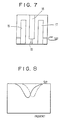
- An example of such a conventional stripline filter device is illustrated in Fig. 1.
- Fig. 1 As will be seen in Fig. 1, it comprises a lower dielectric substrate 1 and an upper dielectric substrate 2 which are stacked to each other.
- Each of the dielectric substrates 1 and 2 may be of dielectric ceramic material having a high dielectric constant and a lower dielectric loss such as BaO-TiO2, BaO-TiO2-rare earth or the like.
- the lower dielectric substrate 1 is provided with an external ground conducting layer 3 on the peripheral portion and bottom surface thereof.
- the upper dielectric substrate 2 is provided with an external ground conducting layer 4 on the peripheral portion and upper surface thereof.
- each resonator conducting layer has one end or an open circuit end (5a, 6a and 7a) spaced from the ground conducting layer 3 and the other end or a short circuit end (5b, 6b and 7b) connected to the ground conducting layer 3.
- the open circuit ends 5a, 6a and 7a of the respective resonator conducting layers 5, 6 and 7 are alternately disposed so as to form an interdigitated configuration.
- the upper dielectric substrate 2 is fixed on the lower dielectric substrate 1, and the ground conducting layers 3 and 4 of the respective dielectric substrates are connected to each other.
- the filter device of this type has a frequency response which depends on the configuration and dielectric constant of the substrates, and the dimension of the resonator conductors.
- the dielectric constant of the substrates and the size of the resonator conducting layers are strictly determined. However, it can not be avoided that there may occur any dispertions in the dielectric constant of the substrates and in the dimension of the resonator conducting layers. It is, therefore, necessary to adjust the frequency response of the filter device after being completed.
- the adjustment of the frequency response can not be performed by adjusting the length of the resonator conducting layers because they are embeded in the dielectric substrates.
- One solution to this problem has been proposed in US Patent No. 4,157,517.
- the frequency of the filter is previously set at a lower level than a desired one, and the external conductor or ground conducting layer provided on the upper surface of the upper substrate is partially removed at regions adjacent the open circuit ends of the resonator conducting layers to reduce the capacitance between the external conducting layer and the respective resonator conducting layers and to increase the response frequency of the filter thereby making it possible to adjust the frequency.
- Another object of the invention is to provide a stripline filter device assembled by using the frequency response adjusting method according to present invention.
- a method of adjusting a frequency response of a stripline filter device which comprises a pair of dielectric substrates each having a peripheral and outer surfaces provided with an external ground conducting layer, and a plurality of stripline resonator conducting layers sandwiched between the dielectric substrates, each resonator conducting layer having a short circuit end connected to the ground conducting layer on one lateral surface of each substrate and an open circuit end spaced from the ground conducting layer on the opposite lateral surface of each substrate, wherein it comprises the steps of electrically connecting the open circuit end of one or more specific resonator conducting layers to the external ground conducting layer on the peripheral surface of each substrate by means of a fine strip member, assembling the dielectric substrates with the resonator conducting layers therebetween, adjusting the frequency response characteristics of the resonator conducting layers provided with no fine strip member at the open circuit ends thereof, and then adjusting sequentially the frequency response characteristics of the resonator conducting layers each provided with the fine strip member by disconnecting the associated fine strip member so as
- each of these resonator conducting layers respectively has no longer resonator function and then will act as an electrical barrier.
- the method of the present invention firstly, one adjusts the frequency response characteristics of the resonator conductor layers whose open ends are not connected to the external ground conducting layer via the fine strip members.
- all the resonator conductor layers are provided with the fine strip members for electrically connecting the open ends thereof to the external ground conducting layer
- the adjusted waveform of the resonator conductor layer is not affected by the adjacent resonator conductor layers because they have the fine strip members provided on the open ends thereof and then will function as the electrical barriers. This in turn allows a frequency response characteristic to be properly adjusted.
- the adjustment of the frequency of each resonator conductor layer may be carried out by removing partially the the ground conducting layer on each substrate as is conventionally known.
- a stripline filter device comprising a pair of dielectric substrates having a peripheral and outer surfaces, an external ground conducting layer provided on the peripheral and outer surfaces of said each dielectric substrate, a plurality of stripline resonator conducting layers sandwiched between said dielectric substrates, each resonator conducting layer having a short circuit end connected to said ground conducting layer on one lateral surface of said each substrate and an open circuit end spaced from said ground conducting layer on the opposite lateral surface of said each substrate, and a fine strip member for electrically connecting the open circuit end of at least one of said resonator conducting layers with the external ground conducting layer, each fine strip member being disconnected when the frequency response of the resonator conducting layer associated therewith is adjusted.
- Figs. 2 and 3 show a stripline filter for which the present invention is applied.
- the illustrated filter comprises a lower and upper dielectric substrates 11 and 12 which are stacked to each other upon the assembling of the filter.
- Each of the dielectric substrates 11 and 12 may be of dielectric ceramic material having a high dielectric constant and a lower dielectric loss such as BaO-TiO2, BaO-TiO2-rare earth or the like.
- the lower dielectric substrate 11 is provided with an external ground conducting layer 13 on the peripheral portion and outer surface thereof.
- the upper dielectric substrate 12 is provided with an external ground conducting layer 14 on the peripheral portion and upper or outer surface thereof.
- each resonator conducting layer has one end or an open circuit end (15a, 16a and 17a) spaced from the ground conducting layer 13 and the other end or a short circuit end (15b, 16b and 17b) connected to the ground conducting layer 13.
- the open circuit ends 15a, 16a and 17a of the respective resonator conducting layers 15, 16 and 17 are alternately disposed so as to form an interdigital type resonator.
- the resonator conducting layers 15 and 17 have lateral extensions 15c and 17c, respectively. These lateral extensions 15c and 17c is connected to signal terminals not shown, respectively.
- the open circuit end 16a of the resonator conducting layers 16 is temporally and electrically connected to the ground conducting layer 13 via a fine strip member 18.
- This fine strip member 18 is so constructed that it can be easily removed at a frequency adjusting procedure and does not affect the characteristic of the the resonator conducting layers 16.
- the upper dielectric substrate 12 may also be provided a plurality of stripline resonator conducting layers 15, 16 and 17 which are disposed to have a reflected image relation with respect to the resonator conducting layers 15, 16 and 17 on the lower dielectric substrate 11.
- the resonator conducting layers 15, 16 and 17 on the lower dielectric substrate 11 becomes into face-to-face contact with those on the upper dielectric substrate 12 without occurring any gaps between the lower dielectric substrate 11 and the upper dielectric substrate 12.
- the ground conducting layers 13 and 14 of the respective dielectric substrates are connected to each other.
- the upper dielectric substrate 12 is also provided with recesses or notches 19 through which the lateral extensions 15c and 17c on the lower dielectric substrate 11 are extended so that they are prevented from bring into contact with the external ground conducting layers 13 and 14.
- the filter device With the filter device thus constructed, it is substantially unavoidable that there may occur any deviations in the dielectric constants of the used substrates and/or in the dimension of the resonator conducting layers upon the manufacturing, which results in that the frequency response of the completed filter may be deviated from an intended one. Therefore, the frequecy response of the filter should be adjusted when being completed.
- a reflection characteristic signal having a waveform S11 from the resonator conducting layer 15 is measured via the lateral extension 15c.
- the adjustment is then carried out for that resonator conducting layer 15 in such a manner that the waveform S11 can be corrected into the curve shown by the solid line. This adjustment can be done by removing partially the external ground conducting layers 13 and 14 on the substrates 11 and 12.
- the external ground conducting layer provided on the peripheral surface of each substrate is partially removed at a portion (13a and 14a) which corresponds to the open circuit end 15a of the resonator conducting layer 15 so as to shift the center frequency toward a higher frequency zone.
- the external ground conducting layer may be partially removed at a portion (13b and 14b) which corresponds to the short circuit end 15b of the resonator conducting layer 15 so as to shift the center frequency toward a lower frequency zone.
- the open circuit end 16a of the central resonator conducting layer 16 is held being connected to the the external ground conducting layers 13 and 14 via the fine strip member 18, and thus, the central resonator conducting layer 16 functions as an electrical barrier.
- the waveform of the frequency response characteristic of the resonator conducting layer 15 can be prevented from being subjected to any influence of the central resonator conducting layer 16 and the other side resonator conducting layer 17.
- a hole 20 is provided at the portion corresponding to one end of the fine strip member 18, thereby cutting off it.
- a reference numeral S21 designates a transmission characteristic of the filter.
- the hole 20 may be provided by means of a laser beam trimming or a rotary whetstone.
- the filter can be tuned to a desired frequency response.
- the upper dielectric substrate 12 is provided with recesses or notches 19 for preventing the lateral extensions 15c and 17c from bring into contact with the external ground conducting layers 13 and 14.
- these recesses 19 may be omitted if the lateral extensions 15c and 17c are extended so that they do not make contact with the external ground conducting layers 13 and 14.
- the resonator conducting layers on the upper dielectric substrate 12 may be omitted if necessary.
- the stripline pattern of the resonator conducting layers 15, 16 and 17 may be formed as a comb type in which the open circuit ends and the short circuit ends thereof are disposed at the same sides, respectively. In that case, the centrally positioned resonator conducting layer should be connected via the fine strip member to the external ground conducting layer.
- the stripline filter is provided with a pair of resonator conducting layers, then the open circuit end of one of these two resonator conducting layers remains being connected with the external ground conducting layer via a fine strip member. In that case, after adjusting the frequency characteristic of the other resonator conducting layer, the fine strip member provided on the the open circuit end of one resonator conducting layer can be cut off and then the frequency adjustment can be performed for this resonator conducting layer.
- a stripline filter device which comprises four or more resonator layers, it is possible to preliminarly provide all the resonator layers with fine strip members, and frequency adjustment for each resonator layer may be sequentially performed by cutting off the associated fine strip member.
- the frequency adjusting is performed for each resonator line under the condition that the resonator conductor(s) adjacent to one to be determined is electrically connected via the fine strip member to the ground layer, and thus the present invention has an advantage that during the frequency adjusting for each resonator line there can be avoided any influence of the other resonator conductor(s).
- the present invention has also an advantage that it is possible to easily and correctly tune the frequency response of the filter device even if the number of the resonator lines is increased.
Landscapes
- Physics & Mathematics (AREA)
- Electromagnetism (AREA)
- Engineering & Computer Science (AREA)
- Manufacturing & Machinery (AREA)
- Control Of Motors That Do Not Use Commutators (AREA)
Applications Claiming Priority (2)
| Application Number | Priority Date | Filing Date | Title |
|---|---|---|---|
| JP2005552A JP2741087B2 (ja) | 1990-01-12 | 1990-01-12 | ストリップラインフィルタの周波数調整法 |
| JP5552/90 | 1990-01-12 |
Publications (3)
| Publication Number | Publication Date |
|---|---|
| EP0437304A2 true EP0437304A2 (de) | 1991-07-17 |
| EP0437304A3 EP0437304A3 (en) | 1992-05-06 |
| EP0437304B1 EP0437304B1 (de) | 1996-03-27 |
Family
ID=11614361
Family Applications (1)
| Application Number | Title | Priority Date | Filing Date |
|---|---|---|---|
| EP91300001A Expired - Lifetime EP0437304B1 (de) | 1990-01-12 | 1991-01-02 | Verfahren zum Einstellen eines Frequenzganges einer Streifenleiterfilteranordnung |
Country Status (4)
| Country | Link |
|---|---|
| US (1) | US5066934A (de) |
| EP (1) | EP0437304B1 (de) |
| JP (1) | JP2741087B2 (de) |
| DE (1) | DE69118212T2 (de) |
Cited By (1)
| Publication number | Priority date | Publication date | Assignee | Title |
|---|---|---|---|---|
| GB2256973A (en) * | 1991-05-15 | 1992-12-23 | Ngk Spark Plug Co | Method of adjusting a frequency response in a microwave strip-line filter device. |
Families Citing this family (5)
| Publication number | Priority date | Publication date | Assignee | Title |
|---|---|---|---|---|
| US5420553A (en) * | 1991-01-16 | 1995-05-30 | Murata Manufacturing Co., Ltd. | Noise filter |
| FI88442C (fi) * | 1991-06-25 | 1993-05-10 | Lk Products Oy | Foerfarande foer foerskjutning av den karakteristika kurvan av en resonator i frekvensplanet och en resonatorkonstruktion |
| JP2657460B2 (ja) * | 1993-10-08 | 1997-09-24 | 富士電気化学株式会社 | 誘電体フィルタの製造方法 |
| JP3144744B2 (ja) * | 1993-11-02 | 2001-03-12 | 日本碍子株式会社 | 積層型誘電体フィルタ |
| JPH08250960A (ja) * | 1995-03-09 | 1996-09-27 | Tdk Corp | フィルタの特性調整方法及びフィルタ |
Family Cites Families (5)
| Publication number | Priority date | Publication date | Assignee | Title |
|---|---|---|---|---|
| US3599124A (en) * | 1968-04-24 | 1971-08-10 | Bell Telephone Labor Inc | Crystal filters |
| US4157517A (en) * | 1977-12-19 | 1979-06-05 | Motorola, Inc. | Adjustable transmission line filter and method of constructing same |
| US4523162A (en) * | 1983-08-15 | 1985-06-11 | At&T Bell Laboratories | Microwave circuit device and method for fabrication |
| US4701727A (en) * | 1984-11-28 | 1987-10-20 | General Dynamics, Pomona Division | Stripline tapped-line hairpin filter |
| JPH01251801A (ja) * | 1988-03-30 | 1989-10-06 | Ngk Spark Plug Co Ltd | 三導体構造フィルタ |
-
1990
- 1990-01-12 JP JP2005552A patent/JP2741087B2/ja not_active Expired - Fee Related
-
1991
- 1991-01-02 DE DE69118212T patent/DE69118212T2/de not_active Expired - Fee Related
- 1991-01-02 EP EP91300001A patent/EP0437304B1/de not_active Expired - Lifetime
- 1991-01-10 US US07/639,352 patent/US5066934A/en not_active Expired - Fee Related
Cited By (2)
| Publication number | Priority date | Publication date | Assignee | Title |
|---|---|---|---|---|
| GB2256973A (en) * | 1991-05-15 | 1992-12-23 | Ngk Spark Plug Co | Method of adjusting a frequency response in a microwave strip-line filter device. |
| GB2256973B (en) * | 1991-05-15 | 1995-03-22 | Ngk Spark Plug Co | Method of adjusting a frequency response in a microwave strip-line filter device |
Also Published As
| Publication number | Publication date |
|---|---|
| US5066934A (en) | 1991-11-19 |
| EP0437304B1 (de) | 1996-03-27 |
| DE69118212T2 (de) | 1996-10-02 |
| JPH03210801A (ja) | 1991-09-13 |
| DE69118212D1 (de) | 1996-05-02 |
| EP0437304A3 (en) | 1992-05-06 |
| JP2741087B2 (ja) | 1998-04-15 |
Similar Documents
| Publication | Publication Date | Title |
|---|---|---|
| EP0396480B1 (de) | Verfahren zum Einstellen des Frequenzganges einer Filtereinrichtung vom Dreileiter-Typ | |
| EP0706230B1 (de) | Funkfrequenzfilter mit helikoidalen Resonatoren | |
| US6462629B1 (en) | Ablative RF ceramic block filters | |
| US6577211B1 (en) | Transmission line, filter, duplexer and communication device | |
| US5525946A (en) | Dielectric resonator apparatus comprising a plurality of one-half wavelength dielectric coaxial resonators having open-circuit gaps at ends thereof | |
| EP1439599B1 (de) | Dielektrisches Filter vom Hohlleitertyp | |
| US5825263A (en) | Low radiation balanced microstrip bandpass filter | |
| US5926078A (en) | Dielectric filter including various means of adjusting the coupling between resonators | |
| EP0343345B1 (de) | Filter in Streifenleiter-Technik | |
| EP0438149B1 (de) | Dielektrisches Filter mit Dämpfungspolen | |
| EP0415558B1 (de) | Bandpassfilter und Verfahren zum Abgleichen von dessen Charakteristika | |
| US5446430A (en) | Folded strip line type dielectric resonator and multilayer dielectric filter using the same | |
| US5039961A (en) | Coplanar attenuator element having tuning stubs | |
| EP0414619B1 (de) | Verfahren zum Einstellen eines Frequenzganges einer Dreileiter-Filteranordnung | |
| EP0437304B1 (de) | Verfahren zum Einstellen eines Frequenzganges einer Streifenleiterfilteranordnung | |
| US6150905A (en) | Dielectric filter with through-hole having large and small diameter portions and a coupling adjustment portion | |
| US4730173A (en) | Asymmetrical trap comprising coaxial resonators, reactance elements, and transmission line elements | |
| US5291162A (en) | Method of adjusting frequency response in a microwave strip-line filter device | |
| WO1994010719A1 (en) | Block filter having high-side passband transfer function zeroes | |
| GB2263583A (en) | Tunable microwave bandstop filter device | |
| US5304966A (en) | Method of adjusting a frequency response in a three-conductor type filter device | |
| US5905415A (en) | Distributed constant line coupling with a gap domain | |
| US5317291A (en) | Microstrip filter with reduced ground plane | |
| US5821835A (en) | Dielectric filter and method of regulating its frequency bandwidth | |
| US6313722B1 (en) | Filter having resonant frequency adjusted with dielectric layer |
Legal Events
| Date | Code | Title | Description |
|---|---|---|---|
| PUAI | Public reference made under article 153(3) epc to a published international application that has entered the european phase |
Free format text: ORIGINAL CODE: 0009012 |
|
| AK | Designated contracting states |
Kind code of ref document: A2 Designated state(s): DE FR GB NL |
|
| PUAL | Search report despatched |
Free format text: ORIGINAL CODE: 0009013 |
|
| AK | Designated contracting states |
Kind code of ref document: A3 Designated state(s): DE FR GB NL |
|
| 17P | Request for examination filed |
Effective date: 19920904 |
|
| 17Q | First examination report despatched |
Effective date: 19940628 |
|
| GRAH | Despatch of communication of intention to grant a patent |
Free format text: ORIGINAL CODE: EPIDOS IGRA |
|
| GRAA | (expected) grant |
Free format text: ORIGINAL CODE: 0009210 |
|
| AK | Designated contracting states |
Kind code of ref document: B1 Designated state(s): DE FR GB NL |
|
| REF | Corresponds to: |
Ref document number: 69118212 Country of ref document: DE Date of ref document: 19960502 |
|
| ET | Fr: translation filed | ||
| PLBE | No opposition filed within time limit |
Free format text: ORIGINAL CODE: 0009261 |
|
| STAA | Information on the status of an ep patent application or granted ep patent |
Free format text: STATUS: NO OPPOSITION FILED WITHIN TIME LIMIT |
|
| 26N | No opposition filed | ||
| REG | Reference to a national code |
Ref country code: GB Ref legal event code: IF02 |
|
| PGFP | Annual fee paid to national office [announced via postgrant information from national office to epo] |
Ref country code: GB Payment date: 20041229 Year of fee payment: 15 |
|
| PGFP | Annual fee paid to national office [announced via postgrant information from national office to epo] |
Ref country code: DE Payment date: 20041231 Year of fee payment: 15 |
|
| PGFP | Annual fee paid to national office [announced via postgrant information from national office to epo] |
Ref country code: NL Payment date: 20050103 Year of fee payment: 15 |
|
| PGFP | Annual fee paid to national office [announced via postgrant information from national office to epo] |
Ref country code: FR Payment date: 20050110 Year of fee payment: 15 |
|
| PG25 | Lapsed in a contracting state [announced via postgrant information from national office to epo] |
Ref country code: GB Free format text: LAPSE BECAUSE OF NON-PAYMENT OF DUE FEES Effective date: 20060102 |
|
| PG25 | Lapsed in a contracting state [announced via postgrant information from national office to epo] |
Ref country code: FR Free format text: LAPSE BECAUSE OF NON-PAYMENT OF DUE FEES Effective date: 20060131 |
|
| PG25 | Lapsed in a contracting state [announced via postgrant information from national office to epo] |
Ref country code: NL Free format text: LAPSE BECAUSE OF NON-PAYMENT OF DUE FEES Effective date: 20060801 Ref country code: DE Free format text: LAPSE BECAUSE OF NON-PAYMENT OF DUE FEES Effective date: 20060801 |
|
| GBPC | Gb: european patent ceased through non-payment of renewal fee |
Effective date: 20060102 |
|
| NLV4 | Nl: lapsed or anulled due to non-payment of the annual fee |
Effective date: 20060801 |
|
| REG | Reference to a national code |
Ref country code: FR Ref legal event code: ST Effective date: 20060929 |