EP0436038A1 - Semiconductor device and method of producing the same - Google Patents
Semiconductor device and method of producing the same Download PDFInfo
- Publication number
- EP0436038A1 EP0436038A1 EP90910930A EP90910930A EP0436038A1 EP 0436038 A1 EP0436038 A1 EP 0436038A1 EP 90910930 A EP90910930 A EP 90910930A EP 90910930 A EP90910930 A EP 90910930A EP 0436038 A1 EP0436038 A1 EP 0436038A1
- Authority
- EP
- European Patent Office
- Prior art keywords
- insulating film
- semiconductor
- layer
- source
- conductivity type
- Prior art date
- Legal status (The legal status is an assumption and is not a legal conclusion. Google has not performed a legal analysis and makes no representation as to the accuracy of the status listed.)
- Withdrawn
Links
- 239000004065 semiconductor Substances 0.000 title claims abstract description 46
- 238000000034 method Methods 0.000 title claims abstract description 23
- 239000000758 substrate Substances 0.000 claims abstract description 26
- 239000012535 impurity Substances 0.000 claims abstract description 14
- VYPSYNLAJGMNEJ-UHFFFAOYSA-N Silicium dioxide Chemical compound O=[Si]=O VYPSYNLAJGMNEJ-UHFFFAOYSA-N 0.000 claims description 6
- 238000005468 ion implantation Methods 0.000 claims description 5
- 239000002052 molecular layer Substances 0.000 claims description 5
- 229910052681 coesite Inorganic materials 0.000 claims description 3
- 229910052906 cristobalite Inorganic materials 0.000 claims description 3
- 239000001301 oxygen Substances 0.000 claims description 3
- 229910052760 oxygen Inorganic materials 0.000 claims description 3
- -1 oxygen ions Chemical class 0.000 claims description 3
- 239000000377 silicon dioxide Substances 0.000 claims description 3
- 235000012239 silicon dioxide Nutrition 0.000 claims description 3
- 229910052682 stishovite Inorganic materials 0.000 claims description 3
- 229910052905 tridymite Inorganic materials 0.000 claims description 3
- 238000010899 nucleation Methods 0.000 claims description 2
- 238000002513 implantation Methods 0.000 claims 1
- 230000000694 effects Effects 0.000 abstract description 5
- 230000005669 field effect Effects 0.000 abstract description 3
- 230000003247 decreasing effect Effects 0.000 abstract 1
- XUIMIQQOPSSXEZ-UHFFFAOYSA-N Silicon Chemical compound [Si] XUIMIQQOPSSXEZ-UHFFFAOYSA-N 0.000 description 6
- 229910052710 silicon Inorganic materials 0.000 description 6
- 239000010703 silicon Substances 0.000 description 6
- 239000007789 gas Substances 0.000 description 3
- 239000013078 crystal Substances 0.000 description 2
- 229910044991 metal oxide Inorganic materials 0.000 description 2
- 150000004706 metal oxides Chemical class 0.000 description 2
- ZOXJGFHDIHLPTG-UHFFFAOYSA-N Boron Chemical compound [B] ZOXJGFHDIHLPTG-UHFFFAOYSA-N 0.000 description 1
- 229910003818 SiH2Cl2 Inorganic materials 0.000 description 1
- 238000000137 annealing Methods 0.000 description 1
- 229910052785 arsenic Inorganic materials 0.000 description 1
- QVGXLLKOCUKJST-UHFFFAOYSA-N atomic oxygen Chemical compound [O] QVGXLLKOCUKJST-UHFFFAOYSA-N 0.000 description 1
- 230000015572 biosynthetic process Effects 0.000 description 1
- 229910052796 boron Inorganic materials 0.000 description 1
- ZOCHARZZJNPSEU-UHFFFAOYSA-N diboron Chemical compound B#B ZOCHARZZJNPSEU-UHFFFAOYSA-N 0.000 description 1
- 239000007772 electrode material Substances 0.000 description 1
- 239000007943 implant Substances 0.000 description 1
- 230000003647 oxidation Effects 0.000 description 1
- 238000007254 oxidation reaction Methods 0.000 description 1
- 230000003071 parasitic effect Effects 0.000 description 1
- 238000004544 sputter deposition Methods 0.000 description 1
Images


Classifications
-
- H—ELECTRICITY
- H01—ELECTRIC ELEMENTS
- H01L—SEMICONDUCTOR DEVICES NOT COVERED BY CLASS H10
- H01L29/00—Semiconductor devices adapted for rectifying, amplifying, oscillating or switching, or capacitors or resistors with at least one potential-jump barrier or surface barrier, e.g. PN junction depletion layer or carrier concentration layer; Details of semiconductor bodies or of electrodes thereof ; Multistep manufacturing processes therefor
- H01L29/66—Types of semiconductor device ; Multistep manufacturing processes therefor
- H01L29/66007—Multistep manufacturing processes
- H01L29/66075—Multistep manufacturing processes of devices having semiconductor bodies comprising group 14 or group 13/15 materials
- H01L29/66227—Multistep manufacturing processes of devices having semiconductor bodies comprising group 14 or group 13/15 materials the devices being controllable only by the electric current supplied or the electric potential applied, to an electrode which does not carry the current to be rectified, amplified or switched, e.g. three-terminal devices
- H01L29/66409—Unipolar field-effect transistors
- H01L29/66477—Unipolar field-effect transistors with an insulated gate, i.e. MISFET
- H01L29/66568—Lateral single gate silicon transistors
- H01L29/66651—Lateral single gate silicon transistors with a single crystalline channel formed on the silicon substrate after insulating device isolation
-
- H—ELECTRICITY
- H01—ELECTRIC ELEMENTS
- H01L—SEMICONDUCTOR DEVICES NOT COVERED BY CLASS H10
- H01L21/00—Processes or apparatus adapted for the manufacture or treatment of semiconductor or solid state devices or of parts thereof
- H01L21/70—Manufacture or treatment of devices consisting of a plurality of solid state components formed in or on a common substrate or of parts thereof; Manufacture of integrated circuit devices or of parts thereof
- H01L21/71—Manufacture of specific parts of devices defined in group H01L21/70
- H01L21/76—Making of isolation regions between components
- H01L21/762—Dielectric regions, e.g. EPIC dielectric isolation, LOCOS; Trench refilling techniques, SOI technology, use of channel stoppers
- H01L21/7624—Dielectric regions, e.g. EPIC dielectric isolation, LOCOS; Trench refilling techniques, SOI technology, use of channel stoppers using semiconductor on insulator [SOI] technology
- H01L21/76243—Dielectric regions, e.g. EPIC dielectric isolation, LOCOS; Trench refilling techniques, SOI technology, use of channel stoppers using semiconductor on insulator [SOI] technology using silicon implanted buried insulating layers, e.g. oxide layers, i.e. SIMOX techniques
-
- H—ELECTRICITY
- H01—ELECTRIC ELEMENTS
- H01L—SEMICONDUCTOR DEVICES NOT COVERED BY CLASS H10
- H01L29/00—Semiconductor devices adapted for rectifying, amplifying, oscillating or switching, or capacitors or resistors with at least one potential-jump barrier or surface barrier, e.g. PN junction depletion layer or carrier concentration layer; Details of semiconductor bodies or of electrodes thereof ; Multistep manufacturing processes therefor
- H01L29/02—Semiconductor bodies ; Multistep manufacturing processes therefor
- H01L29/06—Semiconductor bodies ; Multistep manufacturing processes therefor characterised by their shape; characterised by the shapes, relative sizes, or dispositions of the semiconductor regions ; characterised by the concentration or distribution of impurities within semiconductor regions
- H01L29/0603—Semiconductor bodies ; Multistep manufacturing processes therefor characterised by their shape; characterised by the shapes, relative sizes, or dispositions of the semiconductor regions ; characterised by the concentration or distribution of impurities within semiconductor regions characterised by particular constructional design considerations, e.g. for preventing surface leakage, for controlling electric field concentration or for internal isolations regions
- H01L29/0642—Isolation within the component, i.e. internal isolation
- H01L29/0649—Dielectric regions, e.g. SiO2 regions, air gaps
- H01L29/0653—Dielectric regions, e.g. SiO2 regions, air gaps adjoining the input or output region of a field-effect device, e.g. the source or drain region
-
- H—ELECTRICITY
- H01—ELECTRIC ELEMENTS
- H01L—SEMICONDUCTOR DEVICES NOT COVERED BY CLASS H10
- H01L29/00—Semiconductor devices adapted for rectifying, amplifying, oscillating or switching, or capacitors or resistors with at least one potential-jump barrier or surface barrier, e.g. PN junction depletion layer or carrier concentration layer; Details of semiconductor bodies or of electrodes thereof ; Multistep manufacturing processes therefor
- H01L29/02—Semiconductor bodies ; Multistep manufacturing processes therefor
- H01L29/06—Semiconductor bodies ; Multistep manufacturing processes therefor characterised by their shape; characterised by the shapes, relative sizes, or dispositions of the semiconductor regions ; characterised by the concentration or distribution of impurities within semiconductor regions
- H01L29/10—Semiconductor bodies ; Multistep manufacturing processes therefor characterised by their shape; characterised by the shapes, relative sizes, or dispositions of the semiconductor regions ; characterised by the concentration or distribution of impurities within semiconductor regions with semiconductor regions connected to an electrode not carrying current to be rectified, amplified or switched and such electrode being part of a semiconductor device which comprises three or more electrodes
- H01L29/1025—Channel region of field-effect devices
- H01L29/1029—Channel region of field-effect devices of field-effect transistors
- H01L29/1033—Channel region of field-effect devices of field-effect transistors with insulated gate, e.g. characterised by the length, the width, the geometric contour or the doping structure
- H01L29/105—Channel region of field-effect devices of field-effect transistors with insulated gate, e.g. characterised by the length, the width, the geometric contour or the doping structure with vertical doping variation
-
- H—ELECTRICITY
- H01—ELECTRIC ELEMENTS
- H01L—SEMICONDUCTOR DEVICES NOT COVERED BY CLASS H10
- H01L29/00—Semiconductor devices adapted for rectifying, amplifying, oscillating or switching, or capacitors or resistors with at least one potential-jump barrier or surface barrier, e.g. PN junction depletion layer or carrier concentration layer; Details of semiconductor bodies or of electrodes thereof ; Multistep manufacturing processes therefor
- H01L29/02—Semiconductor bodies ; Multistep manufacturing processes therefor
- H01L29/06—Semiconductor bodies ; Multistep manufacturing processes therefor characterised by their shape; characterised by the shapes, relative sizes, or dispositions of the semiconductor regions ; characterised by the concentration or distribution of impurities within semiconductor regions
- H01L29/10—Semiconductor bodies ; Multistep manufacturing processes therefor characterised by their shape; characterised by the shapes, relative sizes, or dispositions of the semiconductor regions ; characterised by the concentration or distribution of impurities within semiconductor regions with semiconductor regions connected to an electrode not carrying current to be rectified, amplified or switched and such electrode being part of a semiconductor device which comprises three or more electrodes
- H01L29/107—Substrate region of field-effect devices
- H01L29/1075—Substrate region of field-effect devices of field-effect transistors
- H01L29/1079—Substrate region of field-effect devices of field-effect transistors with insulated gate
- H01L29/1083—Substrate region of field-effect devices of field-effect transistors with insulated gate with an inactive supplementary region, e.g. for preventing punch-through, improving capacity effect or leakage current
-
- H—ELECTRICITY
- H01—ELECTRIC ELEMENTS
- H01L—SEMICONDUCTOR DEVICES NOT COVERED BY CLASS H10
- H01L29/00—Semiconductor devices adapted for rectifying, amplifying, oscillating or switching, or capacitors or resistors with at least one potential-jump barrier or surface barrier, e.g. PN junction depletion layer or carrier concentration layer; Details of semiconductor bodies or of electrodes thereof ; Multistep manufacturing processes therefor
- H01L29/66—Types of semiconductor device ; Multistep manufacturing processes therefor
- H01L29/68—Types of semiconductor device ; Multistep manufacturing processes therefor controllable by only the electric current supplied, or only the electric potential applied, to an electrode which does not carry the current to be rectified, amplified or switched
- H01L29/76—Unipolar devices, e.g. field effect transistors
- H01L29/772—Field effect transistors
- H01L29/78—Field effect transistors with field effect produced by an insulated gate
Definitions
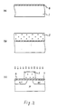
- the process of the prior art for making the metal-oxide semiconductor field effect transistor comprises a step of forming a gate insulating film 4 on a surface portion of a semiconductor substrate 1 as shown in Fig.2 (a), a step of filming a gate electrode material 5 through the gate insulating film 4 as shown in Fig.2 (b), and a step of forming a source 6 and a drain 7 by an ion implantation after having paterned a gate electrode 5 into a predetermined form as shown in Fig.2 (c).
- the drain 7 and the semiconductor substrate 1 has a PN+ junction.
- C D junction capacitance
- An object of the present invention is to provide a MISFET which has a small junction capacitance between the substrate and the drain and improved dynamic characteristics.
- the present invention provides the following means.
- the above embodiments show the formation of MISFET using the semiconductor substrates 1, 31, 41 and 61.
- a well may be used instead of a substrate.
Abstract
An insulated gate field-effect transistor used as a switching element in computers and a method of producing the same. In order to improve dynamic characteristics of the transistor by decreasing the junction capacitance between a substrate (1) and a source (7) or a drain (8), an an insulating layer (2) is provided under the source region and the drain region. In order to decrease the drop of carrier mobility and to suppress the short channel effect, furthermore, the impurity concentration is lowered on the surface of the semiconductor layer just under the gate and is heightened on the side of the substrate.
Description
- The present invention relates to a metal-oxide semiconductor field effect transistor (as will be, hereinafter, abbreviated to "MISFET") which is used as a switching element of a computer.
- The process of the prior art for making the metal-oxide semiconductor field effect transistor ( as will be, hereinafter, abbreviated to "MISFET" ) comprises a step of forming a gate
insulating film 4 on a surface portion of asemiconductor substrate 1 as shown in Fig.2 (a), a step of filming agate electrode material 5 through thegate insulating film 4 as shown in Fig.2 (b), and a step of forming asource 6 and adrain 7 by an ion implantation after having paterned agate electrode 5 into a predetermined form as shown in Fig.2 (c). In this case, thedrain 7 and thesemiconductor substrate 1 has a PN+ junction. - However, a junction capacitance (as will be, hereinafter, called CD for short ) between the substrate and the drain is a factor for dropping the dynamic characteristics of a CMOS inverter, for example, and accordingly has to be reduced.
- An object of the present invention is to provide a MISFET which has a small junction capacitance between the substrate and the drain and improved dynamic characteristics.
- In order to solve the above-specified problems of the prior art, the present invention provides the following means.
- First, an impurity concentration of the surface side portion of the semiconductor layer just under the gate is made low and that of the substrate side portion is made high to prevent short channel effect. In order to realize this structure, the present invention employs either the molecular beam epitaxial growth method (MBE) or the molecular layer epitaxial growth method (MLE) which can accurately control the layer thickness in the order of 0.1 µm or less and also can form a single crystal at low temperature.
- According to the present invention, an
insulating film layer 2 is provided below the source region and the drain region as shown in Fig.1 thereby to reduce the junction capacitance between thesubstrate 1, and thesource 7 and thedrain 8. - Since the impurity concentration is high in the semiconductor layer between the source region and the drain region except the vicinity of the surface, it is possible to reduce the drop of the carrier mobility and to suppress the short-channel effect. Moreover, the junction capacitance between the source and drain regions, and the substrate can be drastically reduced to improve the dynamic characteristics.
-
- Fig.1 is a cross-sectional view showing a structure of a semiconductor device of a first embodiment according to the present invention;
- Fig.2 is a cross-sectional view showing a process flow for making a MISFET according to the prior art;
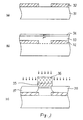
- Figs.3 (a)-(c) are cross-sectional views showing a process flow for making a semiconductor device of a first embodiment according to the present invention;
- Fig.4 is a cross-sectional view showing a process flow of a second embodiment;
- Fig.5 is a graph showing a concentration profile of boron of a semiconductor layer just under a gate in the depth direction in Fig.4(c).
- Figs.6 (a)-(c) are cross-sectional views showing a process flow for making an N channel MISFET of a third embodiment according to the present invention.
- The present invention will be described in detail with reference to the attached drawings.
- A first embodiment of the present invention will be explained with reference to Fig.1 and Figs.3 (a)-(c). As shown in Fig.3 (a), an
insulating film 32 of SiO₂ or SiN etc. is formed on a P type silicon substrate by CVD or thermal oxidation or sputtering, and then is patterned. Next, in Fig.3(b) step, the molecular layer epitaxial growth method is used to form a P+ type epitaxially grownlayer 33 and subsequently a P- type epitaxially grownlayer 34. After this, in Fig.3 (c) step, agate insulating film 35 and agate 36 are formed, and then asource 37 and adrain 38 are formed by ion implantation. The cross-sectional view of the structure of the MOSFET fabricated by the above steps is shown in Fig.1. A first featuring point in Fig.1 is that theinsulating film 2 is formed between the P type silicon substrate and thesource 7 and also between the P type silicon srbstrate and thedrain 8. This point drastically reduces the junction capacitance between the Ptype silicon substrate 1 and thesource 7 and between the Ptype silicon substrate 1 and thedrain 8. A second featuring point in Fig.1 is that the semiconductor layer between thesource 7 and thedrain 8 is composed of the epitaxially grownlayer 3 having a high impurity concentration and the epitaxially grownlayer 4 having a low impurity concentration. In the first embodiment of the present invention, the epitaxially grownlayer 3 has a thickness of about 2,500 Å ,and the epitaxially grownlayer 4 has a thickness of about 700 Å, for example. Since the impurity concentration just below the channel is so high as to suppress extension of a depletion layer from the drain side to the channel side, the structure is hard to invite the short-channel effect. - As has been described herein before, according to the present invention, the junction capacity between the
source 7, thedrain 8 and thesubstrate 1 is drastically reduced to make it possible to improve the dynamic characteristics of the transistor and to realize a MISFET which is excellent in short-channel resistance characteristics. When the lowimpurity concentration layer 4 of the semiconductor layer just under the gate is thicker than the channel and thinner than the depletion layer, a fast operation can be realized. In addition, the threshold voltage of MISFET can be determined by controlling the thickness of thesemiconductor layer 4. An ideal thickness of the low impurity concentration layer is 200 - 800 Å. - Next, a second embodiment of the present invention will be described with reference to Figs.4 and 5. Figs.4 (a)-(c) are cross-sectional views showing a process flow for making a MISFET according to the present invention. In Fig.4 (a) step, an
insulating film 42 is formed on asemiconductor substrate 41 and then etched only at its region just below the portion where a gate will be formed so as to expose the surface of the semiconductor substrate. Next, in Fig.4 (b) step, an epitaxial growth is accomplished by seeding the exposed region of the surface of the semiconductor substrate. In this case, a single crystal is formed by the lateral epitaxial growth on theinsulating film 42 as well. Moreover, if the epitaxial growth is effected by the molecular layer epitaxial method (MLE), the thickness of the epitaxially grown film can be formed in the order of accuracy of a single atomic layer and a profile of impurity concentration becomes steep. In the case of using the molecular layer epitaxial growth method, for example, the profile of the epitaxially grown layer is composed of a P+ layer of about 2,000 Å and P- layer of about 500 Å as shown in Fig.5 and is so steep that the transitional region has a width of about 200 Å. In this case, dicholorosilane gas (SiH₂Cl₂) is used as a source gas of silicon, and diborane (B₂H₆) is used as a doping source to form the P+ layer. However, the P- layer is formed by non-doped growth without diborane gas. Next, in Fig 4 (c) step, agate insulating film 44 and agate electrode 45 are formed, and asource 46 and a drain 47 are then formed by ion implantation. - The MISFET fabricated by the above mentioned method is featured in that the drain capacitance CD is low whereas the current drivability is high. Further, since the impurity concentration just below the channel is high, the drain depletion layer is suppressed from extending to the region just below the gate so that the short channel effect is hard to occur. It is possible to provide a novel method for fabricating a transistor having a low drain capacitance and a high current drivability.
- A third embodiment will be described in detail with reference to Fig.6. Figs.6 (a)-(c) are cross-sectional views showing a process flow for making an N channel MOSFET according to the present invention. Fig.6 (a) shows the state in which a gate
insulating film 62 is formed on asemiconductor substrate 61 of low resistance and in which agate electrode 63 is then patterned by the use of aresist 64. Next, in Fig.6 (b) step, oxygen ions are implanted while leaving theabove resist 64 as it is, to form an SiO₂insulating film 65 below the surface of the semiconductor substrate 61 ( i.e. , closer to the substrate ). After this, theresist 64 is removed, and the damage which has been induced in the surface of thesubstrate 61 at the time of the oxygen ion implantation can be restored by annealing. - After this, as shown in Fig.6 (c), the
resist 64 is removed to implant arsenic ions to formn+ source 66 anddrain 67. The MOSFET thus fabricated is featured in its structure wherein the junction capacitance ( or parasitic capacitance ) between thesemiconductor substrate 61, and thesource 66 and thedrain 67 is small. - Further, the above embodiments show the formation of MISFET using the
semiconductor substrates
Claims (11)
- A semiconductor device in which a gate is formed on the portion between source and drain regions through an insulating film and in which a semiconductor layer just below the gate has a conductivity type opposite to that of the source and drain regions, characterized in that an insulating film is formed below the source and drain regions.
- A semiconductor device according to claim 1, wherein the insulating film layer below the source and drain regions is made of SiO₂ or SiN.
- A semiconductor device according to claim 1,wherein the impurity concentration of the semiconductor layer in the vicinity of the surface is low and that of the bulk side is high.
- A semiconductor device according to claim 3, wherein the semiconductor layer just below the gate comprises plural epitaxially grown layers.
- A semiconductor device according to claim 3, wherein the layer in the vicinity of the surface of the semiconductor layer having low impurity concentration is thinner than a depletion layer.
- A semiconductor device according to claim 3, wherein the thickness of the layer in the vicinity of the surface of the semiconductor layer having low concentration is 200 - 800 Å.
- A method for making a semiconductor device comprising; a first step of forming an insulating film on, at least, a part of a surface of a first conductivity type semiconductor region a second step of providing a semiconductor layer of the same conductivity type as the first conductivity type on the seimconductor region including the insulating film, and a third step of forming a source and a drain of a second conductivity type different from the first conductivity type by an ion implantation after having formed a gate electrode on the semiconductor layer through a gate insulating film, wherein at least the insulating film is provided below the source and the drain.
- A method for making a semiconductor device acccording to claim 7, wherein the second step of providing the first conductivity semiconductor layer is a step to carry out a lateral epitaxial growth seeding the exposed region of the surface of the semiconductor.
- A method for making a semiconductor device according to claim 7, wherein an impurity concentration of the semiconductor layer formed at the second step increases in proportion to a distanc from the gate insulating film.
- A method for making a semiconductor device according to claim 8 or 9, wherein the molecular layer epitaxial growth method or the molecular beam epitaxial growth method is used at the second step of forming the semiconductor layer.
- A method for making a semiconductor comprising; a first step of forming a gate insulating film on a first conductivity type semiconductor substrate and a gate electrode through the gate insulating film, a second step of forming an oxide film below the regions of the semiconductor substrate, where a source and a drain are to be formed by an implantation of oxygen ions while leaving a resist on the gate electrode formed at the first step, and a third step of forming the source and the drain of a second conductivity type by introducing impurity atoms of the second conductivity type different from the first conductivity type.
Applications Claiming Priority (6)
| Application Number | Priority Date | Filing Date | Title |
|---|---|---|---|
| JP18310889A JPH0346371A (en) | 1989-07-14 | 1989-07-14 | Manufacture of semiconductor device |
| JP183108/89 | 1989-07-14 | ||
| JP183106/89 | 1989-07-14 | ||
| JP1183106A JP2869653B2 (en) | 1989-07-14 | 1989-07-14 | Semiconductor device and manufacturing method thereof |
| JP18668189A JPH0350743A (en) | 1989-07-18 | 1989-07-18 | Semiconductor device |
| JP186681/89 | 1989-07-18 |
Publications (2)
| Publication Number | Publication Date |
|---|---|
| EP0436038A1 true EP0436038A1 (en) | 1991-07-10 |
| EP0436038A4 EP0436038A4 (en) | 1991-09-04 |
Family
ID=27325254
Family Applications (1)
| Application Number | Title | Priority Date | Filing Date |
|---|---|---|---|
| EP19900910930 Withdrawn EP0436038A4 (en) | 1989-07-14 | 1990-07-11 | Semiconductor device and method of producing the same |
Country Status (2)
| Country | Link |
|---|---|
| EP (1) | EP0436038A4 (en) |
| WO (1) | WO1991001569A1 (en) |
Cited By (5)
| Publication number | Priority date | Publication date | Assignee | Title |
|---|---|---|---|---|
| FR2673044A1 (en) * | 1991-02-14 | 1992-08-21 | Mitsubishi Electric Corp | FIELD EFFECT TRANSISTOR COMPRISING A BURIED LAYER, AND MANUFACTURING METHOD THEREOF. |
| EP0530046A1 (en) * | 1991-08-30 | 1993-03-03 | STMicroelectronics, Inc. | Integrated circuit transistor |
| EP0535814A1 (en) * | 1991-09-30 | 1993-04-07 | STMicroelectronics, Inc. | Integrated circuit transistor structure and method |
| US5612230A (en) * | 1991-04-16 | 1997-03-18 | Canon Kabushiki Kaisha | Process for manufacturing a semiconductor device by applying a non-single-crystalline material on a sidewall inside of an opening portion for growing a single-crystalline semiconductor body |
| US6064077A (en) * | 1991-08-30 | 2000-05-16 | Stmicroelectronics, Inc. | Integrated circuit transistor |
Citations (5)
| Publication number | Priority date | Publication date | Assignee | Title |
|---|---|---|---|---|
| FR1555057A (en) * | 1967-03-15 | 1969-01-24 | ||
| GB1153428A (en) * | 1965-06-18 | 1969-05-29 | Philips Nv | Improvements in Semiconductor Devices. |
| DE2824419A1 (en) * | 1977-06-03 | 1978-12-07 | Fujitsu Ltd | Semiconductor device and method for the production thereof |
| JPS54159185A (en) * | 1978-06-07 | 1979-12-15 | Fujitsu Ltd | Semiconductor device |
| JPS55121680A (en) * | 1979-03-13 | 1980-09-18 | Nec Corp | Manufacture of semiconductor device |
Family Cites Families (3)
| Publication number | Priority date | Publication date | Assignee | Title |
|---|---|---|---|---|
| JPS56135969A (en) * | 1980-03-27 | 1981-10-23 | Fujitsu Ltd | Manufacture of semiconductor device |
| US4810664A (en) * | 1986-08-14 | 1989-03-07 | Hewlett-Packard Company | Method for making patterned implanted buried oxide transistors and structures |
| JPS63169065A (en) * | 1987-01-05 | 1988-07-13 | Seiko Instr & Electronics Ltd | Insulated gate field effect transistor |
-
1990
- 1990-07-11 WO PCT/JP1990/000889 patent/WO1991001569A1/en not_active Application Discontinuation
- 1990-07-11 EP EP19900910930 patent/EP0436038A4/en not_active Withdrawn
Patent Citations (5)
| Publication number | Priority date | Publication date | Assignee | Title |
|---|---|---|---|---|
| GB1153428A (en) * | 1965-06-18 | 1969-05-29 | Philips Nv | Improvements in Semiconductor Devices. |
| FR1555057A (en) * | 1967-03-15 | 1969-01-24 | ||
| DE2824419A1 (en) * | 1977-06-03 | 1978-12-07 | Fujitsu Ltd | Semiconductor device and method for the production thereof |
| JPS54159185A (en) * | 1978-06-07 | 1979-12-15 | Fujitsu Ltd | Semiconductor device |
| JPS55121680A (en) * | 1979-03-13 | 1980-09-18 | Nec Corp | Manufacture of semiconductor device |
Non-Patent Citations (3)
| Title |
|---|
| PATENT ABSTRACTS OF JAPAN vol. 4, no. 175 (E-36)(657) 03 December 1980, & JP-A-55 121680 (NIPPON DENKI K.K.) 18 September 1980, * |
| PATENT ABSTRACTS OF JAPAN vol. 4, no. 21 (E-172) 21 February 1980, & JP-A-54 159185 (FUJITSU K.K.) 15 December 1979, * |
| See also references of WO9101569A1 * |
Cited By (6)
| Publication number | Priority date | Publication date | Assignee | Title |
|---|---|---|---|---|
| FR2673044A1 (en) * | 1991-02-14 | 1992-08-21 | Mitsubishi Electric Corp | FIELD EFFECT TRANSISTOR COMPRISING A BURIED LAYER, AND MANUFACTURING METHOD THEREOF. |
| US5612230A (en) * | 1991-04-16 | 1997-03-18 | Canon Kabushiki Kaisha | Process for manufacturing a semiconductor device by applying a non-single-crystalline material on a sidewall inside of an opening portion for growing a single-crystalline semiconductor body |
| EP0530046A1 (en) * | 1991-08-30 | 1993-03-03 | STMicroelectronics, Inc. | Integrated circuit transistor |
| US6064077A (en) * | 1991-08-30 | 2000-05-16 | Stmicroelectronics, Inc. | Integrated circuit transistor |
| US6190179B1 (en) | 1991-08-30 | 2001-02-20 | Stmicroelectronics, Inc. | Method of making a field effect transistor having a channel in an epitaxial silicon layer |
| EP0535814A1 (en) * | 1991-09-30 | 1993-04-07 | STMicroelectronics, Inc. | Integrated circuit transistor structure and method |
Also Published As
| Publication number | Publication date |
|---|---|
| WO1991001569A1 (en) | 1991-02-07 |
| EP0436038A4 (en) | 1991-09-04 |
Similar Documents
| Publication | Publication Date | Title |
|---|---|---|
| US6767793B2 (en) | Strained fin FETs structure and method | |
| TWI234283B (en) | Novel field effect transistor and method of fabrication | |
| US5087581A (en) | Method of forming vertical FET device with low gate to source overlap capacitance | |
| JP2929291B2 (en) | Method of manufacturing insulated gate field effect transistor | |
| JP3082671B2 (en) | Transistor element and method of manufacturing the same | |
| KR100237279B1 (en) | Misfet, complementary misfet and manufacturing method thereof | |
| JP3319215B2 (en) | Insulated gate semiconductor device and method of manufacturing the same | |
| US5073519A (en) | Method of fabricating a vertical FET device with low gate to drain overlap capacitance | |
| US6331467B1 (en) | Method of manufacturing a trench gate field effect semiconductor device | |
| US7601996B2 (en) | Semiconductor device and manufacturing method thereof | |
| US11031466B2 (en) | Method of forming oxygen inserted Si-layers in power semiconductor devices | |
| EP0449620B1 (en) | Semiconductor devices having a silicon/silicon-germanium heterostructure and methods of making the same | |
| US6064077A (en) | Integrated circuit transistor | |
| EP0436038A1 (en) | Semiconductor device and method of producing the same | |
| KR930000603B1 (en) | Metal semiconductor field effect transistor | |
| JP3402548B2 (en) | Method for manufacturing semiconductor device | |
| EP0481965B1 (en) | Method of manufacturing step-cut insulated gate static induction transistors | |
| JPH0350771A (en) | Semiconductor device | |
| JP2869653B2 (en) | Semiconductor device and manufacturing method thereof | |
| JPH036863A (en) | Semiconductor device | |
| JPS63142677A (en) | Insulated-gate field-effect transistor | |
| JPS59149059A (en) | Metal insulator semiconductor transistor and manufacture thereof | |
| JPH03793B2 (en) | ||
| JP3467288B2 (en) | Vertical junction field-effect transistor with optimized bipolar operation mode and method of manufacturing the same | |
| JPH0290537A (en) | Semiconductor device |
Legal Events
| Date | Code | Title | Description |
|---|---|---|---|
| PUAI | Public reference made under article 153(3) epc to a published international application that has entered the european phase |
Free format text: ORIGINAL CODE: 0009012 |
|
| 17P | Request for examination filed |
Effective date: 19910312 |
|
| AK | Designated contracting states |
Kind code of ref document: A1 Designated state(s): DE FR GB NL |
|
| A4 | Supplementary search report drawn up and despatched |
Effective date: 19910712 |
|
| AK | Designated contracting states |
Kind code of ref document: A4 Designated state(s): DE FR GB NL |
|
| STAA | Information on the status of an ep patent application or granted ep patent |
Free format text: STATUS: THE APPLICATION IS DEEMED TO BE WITHDRAWN |
|
| 18D | Application deemed to be withdrawn |
Effective date: 19930202 |