EP0435581A2 - Output amplifying stage with power saving feature - Google Patents
Output amplifying stage with power saving feature Download PDFInfo
- Publication number
- EP0435581A2 EP0435581A2 EP90314039A EP90314039A EP0435581A2 EP 0435581 A2 EP0435581 A2 EP 0435581A2 EP 90314039 A EP90314039 A EP 90314039A EP 90314039 A EP90314039 A EP 90314039A EP 0435581 A2 EP0435581 A2 EP 0435581A2
- Authority
- EP
- European Patent Office
- Prior art keywords
- output
- sense amplifier
- amplifier
- memory
- response
- Prior art date
- Legal status (The legal status is an assumption and is not a legal conclusion. Google has not performed a legal analysis and makes no representation as to the accuracy of the status listed.)
- Granted
Links
Images
Classifications
-
- G—PHYSICS
- G11—INFORMATION STORAGE
- G11C—STATIC STORES
- G11C11/00—Digital stores characterised by the use of particular electric or magnetic storage elements; Storage elements therefor
- G11C11/21—Digital stores characterised by the use of particular electric or magnetic storage elements; Storage elements therefor using electric elements
- G11C11/34—Digital stores characterised by the use of particular electric or magnetic storage elements; Storage elements therefor using electric elements using semiconductor devices
- G11C11/40—Digital stores characterised by the use of particular electric or magnetic storage elements; Storage elements therefor using electric elements using semiconductor devices using transistors
- G11C11/401—Digital stores characterised by the use of particular electric or magnetic storage elements; Storage elements therefor using electric elements using semiconductor devices using transistors forming cells needing refreshing or charge regeneration, i.e. dynamic cells
- G11C11/4063—Auxiliary circuits, e.g. for addressing, decoding, driving, writing, sensing or timing
- G11C11/407—Auxiliary circuits, e.g. for addressing, decoding, driving, writing, sensing or timing for memory cells of the field-effect type
- G11C11/409—Read-write [R-W] circuits
-
- G—PHYSICS
- G11—INFORMATION STORAGE
- G11C—STATIC STORES
- G11C7/00—Arrangements for writing information into, or reading information out from, a digital store
- G11C7/22—Read-write [R-W] timing or clocking circuits; Read-write [R-W] control signal generators or management
-
- G—PHYSICS
- G11—INFORMATION STORAGE
- G11C—STATIC STORES
- G11C7/00—Arrangements for writing information into, or reading information out from, a digital store
- G11C7/06—Sense amplifiers; Associated circuits, e.g. timing or triggering circuits
-
- G—PHYSICS
- G11—INFORMATION STORAGE
- G11C—STATIC STORES
- G11C7/00—Arrangements for writing information into, or reading information out from, a digital store
- G11C7/10—Input/output [I/O] data interface arrangements, e.g. I/O data control circuits, I/O data buffers
- G11C7/1051—Data output circuits, e.g. read-out amplifiers, data output buffers, data output registers, data output level conversion circuits
Definitions
- the invention relates memories, and more particularly, to the output amplifying stage of a memory.
- One of the critical aspects of a memory is the signal path from a selected memory cell to the output.
- the memory cell produces a relatively small signal to indicate a particular logic state which comprises one bit of information.
- This small signal is amplified through a number of stages and finally output as a relatively strong output signal.
- the strength of the signal primarily relates to voltage level and current drive capability.
- the signal from the memory cell is generally weak in both voltage and current drive, and thus the need for amplification. This amplification is necessary, but the amplification path is also a critical path in determining the speed with which the memory can operate. Thus, it is desirable to perform the needed amplification as quickly as possible. Generally, there is a speed/power tradeoff.
- the speed of amplification for a particular circuit type can be increased but at the cost of using more power.
- the active power tends to increase as the frequency increases.
- the memory is using maximum power for a given power supply voltage.
- the maximum power that can be consumed is a function of how well heat can be dissipated. If the heat becomes too great, the memory can experience various problems including actually permanently damaging the particular memory device. Thus, it is desirable to save power whenever it is feasible, especially if it can be done without degrading the performance of the memory device.
- the amplification stage is a major contributor to the overall power consumed by the device. This is due to a large extent because speed of amplification is so important.
- power saving techniques available but they generally have only nominal affect at the higher frequencies of operation.
- One such technique is to power down the amplifier stage some predetermined time after an address transition.
- Another approach has been to power-up the sense amplifier stage with a transition signal initiated by an address transition, detect when the output is valid, and disable the transition signal in response to detecting that the output is valid.
- Another object of the invention is to provide an improved output amplifier of a memory with power saving feature.
- a memory having an array of memory cells, each memory cell for containing data therein; decoder means for selecting a memory cell in response to an address; a first sense amplifier for receiving data from the selected memory cell and for providing an output representative of the data received from the selected memory cell; a second sense amplifier for receiving the output of the first sense amplifier and for providing an output; and an output driver for receiving the output of the second sense amplifier and for providing an output of the memory, comprising: detection means for providing a detection signal in response to the output of the second sense amplifier being valid; first control means, coupled to the detection means and the first sense amplifier, for enabling the first sense amplifier in response to a transition of the address and disabling the first sense amplifier in response to the detection signal; and second control means, coupled to the second sense amplifier, for disabling the second sense amplifier for at least a predetermined time after the first sense amplifier has been enabled and enabling the second sense amplifier after the predetermined time.
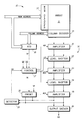
- the figure is a block diagram of a memory according to a preferred embodiment of the invention.
- FIG. 1 Shown in FIG. 1 is a memory 10 comprised generally of an array 11, a row decoder 12, a column decoder 13, an amplification stage 14, an address transition detector (ATD) 16, a control circuit 17, a preset circuit 18, and a detector 19.
- Amplification stage 14 comprises an amplifier 21, a level shifter 22, an amplifier 23, a level shifter 24, an amplifier 25, and an output driver 26.
- Array 11 contains a plurality of static random access memory (SRAM) cells located at intersections of word lines and bit line pairs.
- Row decoder 12 selects a word line in array 11 as determined by a row address.
- SRAM static random access memory
- amplifier 21 The data contained in the memory cell coupled to the selected word line and to the selected bit line pair is thereby communicated to amplifier 21 in the form of a voltage differential developed on the selected bit line pair.
- amplifier 21 When enabled by an amplifier enable signal AE1 being active, amplifier 21 amplifies the voltage differential input thereto and provides an amplified voltage differential to level shifter 22.
- level shifter 22 When enabled by a level shift enable signal LE1 being active, level shifter 22 shifts the voltage level of the voltage differential provided by amplifier 21 and outputs the level-shifted voltage differential to amplifier amplifier 23.
- amplifier 23 When enabled by an amplifier enable signal AE2 being active, amplifier 23 amplifies the level-shifted voltage differential provided by level shifter 22 and provides an amplified voltage differential to level shifter 24.
- level shifter 24 shifts the voltage level of the voltage differential provided by amplifier 23 and outputs the level-shifted voltage differential to amplifier amplifier 25.
- amplifier 25 amplifies the level-shifted voltage differential provided by level shifter 24 and provides an amplified voltage differential to output driver 26 which provides a data output signal DO representative of the logic state of the selected memory cell.
- Amplifier stage 14 is active only when memory 10 is in the read mode and is selected to be active.
- Memory 10 is placed into the read mode under the control of the write enable signal WE and is selected to be active under the control of a chip select signal CS .
- Memory 10 is in the read mode when write enable signal WE is a logic high and chip select signal CS is a logic low.
- Control circuit 17 provides signals PE, AE1, AE2, and LE1 in either an active state or an inactive state. If memory 10 is not in the read mode, control circuit 17 provides signals PE, AE1, AE2, and LE1 in the inactive state. In the read mode control circuit 17 provides signals PE, AE1, AE2, and LE1 in the active state in response to transition pulse TP becoming active. Control circuit 17 responds to a data valid signal DV being active by making signals PE, AE1, AE2, and LE1 inactive.
- Preset Circuit 18 provides signal AE3 in either an active or an inactive state under the control of transition pulse TP and preset enable signal PE.
- Preset circuit 18 provides signal AE3 in an inactive state in response to signal PE being provided in an inactive state.
- signal PE is active
- signal AE3 will be provided in the active state a predetermined time following transition pulse TP becoming active. This predetermined time is conveniently a delay period following transition pulse becoming inactive.
- preset circuit 18 clamps both outputs of amplifier 25 to ground in response to signal TP being active and releases this clamping so that the output of amplifier 25 can become valid in response to transition pulse TP becoming inactive.
- ATD circuit 16 provides transition pulse TP in an active state for any address transition, either row or column, for about 5 nanoseconds.
- Detector 19 detects when the outputs of amplifier 25 provide a sufficient voltage differential to be considered valid data. When the output of amplifier 25 is thus detected as valid, detector 19 provides signal DV in an active state, otherwise detector 19 provides signal DV in an inactive state.
- output driver 26 Prior to an address transition but after a read has been performed, output driver 26 has latched the logic state of the selected memory cell and is providing output signal DO at the logic state representative of the selected memory cell. In this condition, detector 19 has detected that the output of amplifier 25 had been valid and thus provided signal DV in an active state. Pulse TP is inactive so that control circuit 17 is providing signals AE1, AE2, PE, and LE1 in an inactive state. Thus, amplifier 21, level shifter 22, amplifier 23, and level shifter 24 are disabled. Similarly, preset circuit 18 is providing signal AE3 in an inactive state which results in amplifier 25 being disabled.
- ATD circuit 16 To select a different memory cell, there will be an address transition which is detected by ATD circuit 16. While the memory cell is being selected, ATD circuit 16 generates transition pulse TP. Control circuit 17 responds by activating amplifier 21, level shifter 22, amplifier 23, and level shifter 24 by providing signals AE1, AE2, and LE1 in an active state. Thus, by the time the newly selected cell is providing a voltage differential to amplifier 21, amplifier 21 is enabled and ready to amplify the newly provided voltage differential. Control circuit 17 also responds by providing signal PE in an active state. Preset circuit 18 is thus simultaneously receiving signal PE and pulse TP in their respective active states. Preset circuit 18 responds by maintaining signal AE3 in the inactive state and clamping the outputs of amplifier 25 to an invalid state.
- detector 19 With amplifier 25 providing an invalid output, detector 19 provides signal DV in the inactive state.
- Amplifiers 21 and 23 and level shifters 22 and 24 provide their respective amplification and level shifting functions while pulse TP is active and amplifier 25 is disabled. After a short delay time following the termination of pulse TP, preset circuit 18 outputs signal AE3 in an active state and terminates the clamping of the output of amplifier 25.
- amplifier 25 is enabled and can provide an amplified voltage differential to output driver 26.
- detector 19 When amplifier 25 does provide a voltage differential detected by detector 19, detector 19 responds by providing signal DV in the active state which causes control circuit 17 to provide signals PE, AE1, AE2, and LE1 in the inactive state which in turn disables amplifiers 21 and 23 and level shifters 22 and 24. Preset circuit 18 responds to signal PE being inactive by providing signal AE3 in the inactive state and thus disabling amplifier 25.
- Output driver 26 includes a latch which latches the output of amplifier 25 in response to the data provided by amplifier 25 being valid. This latching action of output driver 26 is released in response to a new address transition.
- This latch of output driver 26 is disabled in response to an address transition and enabled in response to the output of amplifier 25 which is thus complementary in operation to the operation of amplifiers 21 and 23 and level shifters 22 and 24 which are active in response to an address transition and disabled in response to the output of amplifier 25 being valid.
- the control of this latching operation of output driver 26 is not shown in the figure.
- Amplification stage 14 can thus be viewed as divided into three stages.
- Amplifiers 21 and 23 and level shifters 22 and 24 can be viewed as a first stage of amplification that begins amplifying in response to an address transition.
- Amplifier 25 can be viewed as a second stage of amplification which is disabled for a predetermined delay time after the first stage is enabled and then enabled. There is thus a time during which the first stage is enabled and the second stage is disabled. During this time period, the output of the second stage is clamped to an invalid state and released thereafter.
- Output driver 26 can be viewed as the the third stage which responds to the output of the second stage and provides an output of the memory. Both the first and second amplification stages are disabled in response to the output of the second stage becoming valid.
- the timing of the enabling of amplifier 25 can be adjusted so there is no delay in the propagation of the differential signal to the output of amplifier 25 but also that the first amplification stage has resolved which direction the differential voltage will be provided.
- that imbalance will not be provided to the output of amplifier 25 because amplifier 25 is disabled and its output is clamped during the initial time period.
- the second amplification stage is enabled and its output released, the first amplification stage has fully resolved the output that is to be provided.
- amplifier 25 never provides an output that is invalid except when it is clamped to the particular known invalid state.
- detector 19 can be made as sensitive as desirable in detecting a differential at the output of amplifier 25 without concern that the output would be providing a false voltage differential.
Abstract
Description
- The invention relates memories, and more particularly, to the output amplifying stage of a memory.
- One of the critical aspects of a memory is the signal path from a selected memory cell to the output. The memory cell produces a relatively small signal to indicate a particular logic state which comprises one bit of information. This small signal is amplified through a number of stages and finally output as a relatively strong output signal. The strength of the signal primarily relates to voltage level and current drive capability. The signal from the memory cell is generally weak in both voltage and current drive, and thus the need for amplification. This amplification is necessary, but the amplification path is also a critical path in determining the speed with which the memory can operate. Thus, it is desirable to perform the needed amplification as quickly as possible. Generally, there is a speed/power tradeoff. Thus, the speed of amplification for a particular circuit type can be increased but at the cost of using more power. There are two major components of power usage, standby and active. The active power tends to increase as the frequency increases. Thus, at some maximum frequency of operation, the memory is using maximum power for a given power supply voltage. The maximum power that can be consumed is a function of how well heat can be dissipated. If the heat becomes too great, the memory can experience various problems including actually permanently damaging the particular memory device. Thus, it is desirable to save power whenever it is feasible, especially if it can be done without degrading the performance of the memory device.
- The amplification stage, particularly at high frequency, is a major contributor to the overall power consumed by the device. This is due to a large extent because speed of amplification is so important. There are power saving techniques available but they generally have only nominal affect at the higher frequencies of operation. One such technique is to power down the amplifier stage some predetermined time after an address transition. Another approach has been to power-up the sense amplifier stage with a transition signal initiated by an address transition, detect when the output is valid, and disable the transition signal in response to detecting that the output is valid. This is described in "Two Novel Power-Down Circuits on the 1 Mb CMOS SRAM," by Masataka Matsui, et al., in the 1988 Symposium On VLSI Circuits, Digest of Technical Papers, Circuits Symposium, Tokyo, IEEE Cat. No. 88 Th 0227-9, pages 55 and 56. This approach continues to offer power-savings benefits even at higher frequencies. There are, however, some problems with this approach. One problem is that the data can give a false reading of validity. The point in the amplification stage at which the validity is detected may have a voltage movement which is sufficient to cause the validity detector to falsely detect that the data is valid. This can happen due to noise in the system which is amplified or to unbalanced bit lines which begin with a differential which opposite to that which will be eventually established for valid data. If the detector falsely detects that the data is valid, the sense amplifier will be disabled prematurely.
- Accordingly, it is an object of the present invention to provide an improved output amplifying stage for a memory.
- Another object of the invention is to provide an improved output amplifier of a memory with power saving feature.
- In carrying out these and other objects of the invention, there is provided, in one form, a memory having an array of memory cells, each memory cell for containing data therein; decoder means for selecting a memory cell in response to an address; a first sense amplifier for receiving data from the selected memory cell and for providing an output representative of the data received from the selected memory cell; a second sense amplifier for receiving the output of the first sense amplifier and for providing an output; and an output driver for receiving the output of the second sense amplifier and for providing an output of the memory, comprising:
detection means for providing a detection signal in response to the output of the second sense amplifier being valid;
first control means, coupled to the detection means and the first sense amplifier, for enabling the first sense amplifier in response to a transition of the address and disabling the first sense amplifier in response to the detection signal; and
second control means, coupled to the second sense amplifier, for disabling the second sense amplifier for at least a predetermined time after the first sense amplifier has been enabled and enabling the second sense amplifier after the predetermined time. - The figure is a block diagram of a memory according to a preferred embodiment of the invention.
- Shown in FIG. 1 is a
memory 10 comprised generally of anarray 11, arow decoder 12, acolumn decoder 13, anamplification stage 14, an address transition detector (ATD) 16, acontrol circuit 17, apreset circuit 18, and adetector 19.Amplification stage 14 comprises anamplifier 21, alevel shifter 22, anamplifier 23, alevel shifter 24, anamplifier 25, and anoutput driver 26.Array 11 contains a plurality of static random access memory (SRAM) cells located at intersections of word lines and bit line pairs.Row decoder 12 selects a word line inarray 11 as determined by a row address. Whenmemory 10 is in a read mode as indicated by signalWE being at a logic high,column decoder 13 couples a selected bit line pair, as determined by a column address, to amplifier. The data contained in the memory cell coupled to the selected word line and to the selected bit line pair is thereby communicated to amplifier 21 in the form of a voltage differential developed on the selected bit line pair. When enabled by an amplifier enable signal AE1 being active,amplifier 21 amplifies the voltage differential input thereto and provides an amplified voltage differential tolevel shifter 22. When enabled by a level shift enable signal LE1 being active,level shifter 22 shifts the voltage level of the voltage differential provided byamplifier 21 and outputs the level-shifted voltage differential toamplifier amplifier 23. When enabled by an amplifier enable signal AE2 being active,amplifier 23 amplifies the level-shifted voltage differential provided bylevel shifter 22 and provides an amplified voltage differential tolevel shifter 24. When enabled by amplifier enable signal AE2 being active,level shifter 24 shifts the voltage level of the voltage differential provided byamplifier 23 and outputs the level-shifted voltage differential toamplifier amplifier 25. When enabled by an amplifier enable signal AE3 being active,amplifier 25 amplifies the level-shifted voltage differential provided bylevel shifter 24 and provides an amplified voltage differential tooutput driver 26 which provides a data output signal DO representative of the logic state of the selected memory cell. -
Amplifier stage 14 is active only whenmemory 10 is in the read mode and is selected to be active.Memory 10 is placed into the read mode under the control of the write enable signalWE and is selected to be active under the control of a chip select signalCS .Memory 10 is in the read mode when write enable signalWE is a logic high and chip select signalCS is a logic low.Control circuit 17 provides signals PE, AE1, AE2, and LE1 in either an active state or an inactive state. Ifmemory 10 is not in the read mode,control circuit 17 provides signals PE, AE1, AE2, and LE1 in the inactive state. In the readmode control circuit 17 provides signals PE, AE1, AE2, and LE1 in the active state in response to transition pulse TP becoming active.Control circuit 17 responds to a data valid signal DV being active by making signals PE, AE1, AE2, and LE1 inactive. - Preset
Circuit 18 provides signal AE3 in either an active or an inactive state under the control of transition pulse TP and preset enable signal PE.Preset circuit 18 provides signal AE3 in an inactive state in response to signal PE being provided in an inactive state. For the case in which signal PE is active, signal AE3 will be provided in the active state a predetermined time following transition pulse TP becoming active. This predetermined time is conveniently a delay period following transition pulse becoming inactive. In the readmode preset circuit 18 clamps both outputs ofamplifier 25 to ground in response to signal TP being active and releases this clamping so that the output ofamplifier 25 can become valid in response to transition pulse TP becoming inactive.ATD circuit 16 provides transition pulse TP in an active state for any address transition, either row or column, for about 5 nanoseconds.Detector 19 detects when the outputs ofamplifier 25 provide a sufficient voltage differential to be considered valid data. When the output ofamplifier 25 is thus detected as valid,detector 19 provides signal DV in an active state, otherwisedetector 19 provides signal DV in an inactive state. - Prior to an address transition but after a read has been performed,
output driver 26 has latched the logic state of the selected memory cell and is providing output signal DO at the logic state representative of the selected memory cell. In this condition,detector 19 has detected that the output ofamplifier 25 had been valid and thus provided signal DV in an active state. Pulse TP is inactive so thatcontrol circuit 17 is providing signals AE1, AE2, PE, and LE1 in an inactive state. Thus,amplifier 21,level shifter 22,amplifier 23, andlevel shifter 24 are disabled. Similarly,preset circuit 18 is providing signal AE3 in an inactive state which results inamplifier 25 being disabled. - To select a different memory cell, there will be an address transition which is detected by
ATD circuit 16. While the memory cell is being selected,ATD circuit 16 generates transition pulse TP.Control circuit 17 responds by activatingamplifier 21,level shifter 22,amplifier 23, andlevel shifter 24 by providing signals AE1, AE2, and LE1 in an active state. Thus, by the time the newly selected cell is providing a voltage differential toamplifier 21,amplifier 21 is enabled and ready to amplify the newly provided voltage differential.Control circuit 17 also responds by providing signal PE in an active state. Presetcircuit 18 is thus simultaneously receiving signal PE and pulse TP in their respective active states. Presetcircuit 18 responds by maintaining signal AE3 in the inactive state and clamping the outputs ofamplifier 25 to an invalid state. Withamplifier 25 providing an invalid output,detector 19 provides signal DV in the inactive state.Amplifiers level shifters amplifier 25 is disabled. After a short delay time following the termination of pulse TP,preset circuit 18 outputs signal AE3 in an active state and terminates the clamping of the output ofamplifier 25. Thus, by thetime level shifter 24 is providing a valid voltage differential derived from the newly selected cell,amplifier 25 is enabled and can provide an amplified voltage differential tooutput driver 26. Whenamplifier 25 does provide a voltage differential detected bydetector 19,detector 19 responds by providing signal DV in the active state which causescontrol circuit 17 to provide signals PE, AE1, AE2, and LE1 in the inactive state which in turn disablesamplifiers level shifters circuit 18 responds to signal PE being inactive by providing signal AE3 in the inactive state and thus disablingamplifier 25.Output driver 26 includes a latch which latches the output ofamplifier 25 in response to the data provided byamplifier 25 being valid. This latching action ofoutput driver 26 is released in response to a new address transition. This latch ofoutput driver 26 is disabled in response to an address transition and enabled in response to the output ofamplifier 25 which is thus complementary in operation to the operation ofamplifiers level shifters amplifier 25 being valid. The control of this latching operation ofoutput driver 26 is not shown in the figure. -
Amplification stage 14 can thus be viewed as divided into three stages.Amplifiers level shifters Amplifier 25 can be viewed as a second stage of amplification which is disabled for a predetermined delay time after the first stage is enabled and then enabled. There is thus a time during which the first stage is enabled and the second stage is disabled. During this time period, the output of the second stage is clamped to an invalid state and released thereafter.Output driver 26 can be viewed as the the third stage which responds to the output of the second stage and provides an output of the memory. Both the first and second amplification stages are disabled in response to the output of the second stage becoming valid. This saves substantial current in the first and second amplification stages. Furthermore, the timing of the enabling ofamplifier 25 can be adjusted so there is no delay in the propagation of the differential signal to the output ofamplifier 25 but also that the first amplification stage has resolved which direction the differential voltage will be provided. Thus, although there may be an initial imbalance through the first amplification stage, that imbalance will not be provided to the output ofamplifier 25 becauseamplifier 25 is disabled and its output is clamped during the initial time period. By the time the second amplification stage is enabled and its output released, the first amplification stage has fully resolved the output that is to be provided. Thus,amplifier 25 never provides an output that is invalid except when it is clamped to the particular known invalid state. Thus,detector 19 can be made as sensitive as desirable in detecting a differential at the output ofamplifier 25 without concern that the output would be providing a false voltage differential. - While the invention has been described in a specific embodiment, it will be apparent to those skilled in the art that the disclosed invention may be modified in numerous ways and may assume many embodiments other than those specifically set out and described above. For example, more or less stages of amplification could be employed. Accordingly, it is intended by the appended claims to cover all modifications of the invention which fall within the true spirit and scope of the invention.
Claims (7)
- A memory (10) having an array of memory cells (11), each memory cell for containing data therein; decoder means (12, 13) for selecting a memory cell in response to an address; a first sense amplifier (21) for receiving data from the selected memory cell and for providing an output representative of the data received from the selected memory cell; a second sense amplifier (25) for receiving the output of the first sense amplifier (21) and for providing an output; and an output driver (26) for receiving the output of the second sense amplifier (25) and for providing an output of the memory, comprising:
detection means (19) for providing a detection signal in response to the output of the second sense amplifier (25) being valid;
first control means (17), coupled to the detection means and the first sense amplifier (21), for enabling the first sense amplifier (21) in response to a transition of the address and disabling the first sense amplifier (21) in response to the detection signal; and
second control means(18), coupled to the second sense amplifier(25), for disabling the second sense amplifier (25) for at least a predetermined time after the first sense amplifier (21) has been enabled and enabling the second sense amplifier (25) after the predetermined time. - The memory of claim 1, wherein the second control means (18) is further characterized as clamping the output of the second sense amplifier (25) to an invalid state in response to an address transition.
- The memory of claim 2, wherein the second control means (18) is further characterized as releasing the output of the second sense amplifier (25) when the second sense amplifier (25) is enabled.
- The memory of claim 1 or 2, wherein the second control means (18) is further characterized as disabling the second sense amplifier (25) in response to the detection signal.
- The memory of claim 1 wherein the output of the first sense amplifier is coupled to the second sense amplifier via a first level shifter, a third sense amplifier, and a second level shifter.
- In a memory having an array of memory cells, each memory cell for containing data therein; decoder means for selecting a memory cell in response to an address; a first sense amplifier for receiving data from the selected memory cell and for providing an output representative of the data received from the selected memory cell; a second sense amplifier for receiving the output of the first sense amplifier and for providing an output; an output driver for receiving the output of the second sense amplifier and for providing an output of the memory; a method for enabling and disabling the first and second sense amplifier, comprising the steps of:
enabling the first sense amplifier in response to a transition of the address;
disabling the second sense amplifier for at least a predetermined time after the first sense amplifier has been enabled;
enabling the second sense amplifier after the predetermined time; and
disabling the first sense amplifier in response to detecting that the output of the second sense amplifier is valid. - The method of claim 6 further comprising the step of disabling the second sense amplifier in response to detecting that the output of the second sense amplifier is valid.
Applications Claiming Priority (2)
| Application Number | Priority Date | Filing Date | Title |
|---|---|---|---|
| US07/457,646 US4972374A (en) | 1989-12-27 | 1989-12-27 | Output amplifying stage with power saving feature |
| US457646 | 1999-12-09 |
Publications (3)
| Publication Number | Publication Date |
|---|---|
| EP0435581A2 true EP0435581A2 (en) | 1991-07-03 |
| EP0435581A3 EP0435581A3 (en) | 1992-06-03 |
| EP0435581B1 EP0435581B1 (en) | 1997-05-14 |
Family
ID=23817581
Family Applications (1)
| Application Number | Title | Priority Date | Filing Date |
|---|---|---|---|
| EP90314039A Expired - Lifetime EP0435581B1 (en) | 1989-12-27 | 1990-12-20 | Output amplifying stage with power saving feature |
Country Status (5)
| Country | Link |
|---|---|
| US (1) | US4972374A (en) |
| EP (1) | EP0435581B1 (en) |
| JP (1) | JPH04364296A (en) |
| KR (1) | KR910013281A (en) |
| DE (1) | DE69030716D1 (en) |
Cited By (1)
| Publication number | Priority date | Publication date | Assignee | Title |
|---|---|---|---|---|
| EP0827151A1 (en) * | 1996-08-28 | 1998-03-04 | Nec Corporation | Self cut-off type sense amplifier operable over a wide range of power supply voltages |
Families Citing this family (26)
| Publication number | Priority date | Publication date | Assignee | Title |
|---|---|---|---|---|
| JPH03152794A (en) * | 1989-11-09 | 1991-06-28 | Nec Ic Microcomput Syst Ltd | Semiconductor memory device |
| US5485418A (en) * | 1990-01-16 | 1996-01-16 | Mitsubishi Denki Kabushiki Kaisha | Associative memory |
| JP2685656B2 (en) * | 1990-12-28 | 1997-12-03 | サムサン エレクトロニクス シーオー., エルティーディー | Output control circuit of sense amplifier |
| JPH04341997A (en) * | 1991-05-20 | 1992-11-27 | Mitsubishi Electric Corp | Semiconductor memory device |
| EP0527015A2 (en) * | 1991-08-06 | 1993-02-10 | AT&T Corp. | Low power signaling using output impedance delay |
| KR940010838B1 (en) * | 1991-10-28 | 1994-11-17 | 삼성전자 주식회사 | Data output control circuit |
| JPH05325569A (en) * | 1992-05-27 | 1993-12-10 | Toshiba Corp | Semiconductor storage device |
| US5651126A (en) * | 1992-06-26 | 1997-07-22 | Apple Computer, Inc. | Method and apparatus for reducing transitions on computer signal lines |
| JP3212396B2 (en) * | 1993-01-14 | 2001-09-25 | 富士通株式会社 | Nonvolatile semiconductor memory device |
| US5377143A (en) * | 1993-03-31 | 1994-12-27 | Sgs-Thomson Microelectronics, Inc. | Multiplexing sense amplifier having level shifter circuits |
| JP3307009B2 (en) * | 1993-07-21 | 2002-07-24 | 富士通株式会社 | Semiconductor storage device |
| KR970001345B1 (en) * | 1993-07-28 | 1997-02-05 | 삼성전자 주식회사 | Level shifter |
| JP2687852B2 (en) * | 1993-10-13 | 1997-12-08 | 日本電気株式会社 | Semiconductor memory device |
| US5563835A (en) * | 1994-01-31 | 1996-10-08 | Advanced Risc Machines Limited | Sense amplification in data memories |
| GB2286272A (en) * | 1994-01-31 | 1995-08-09 | Advanced Risc Mach Ltd | Data memory sense amplifier operation |
| JPH08235865A (en) * | 1995-02-28 | 1996-09-13 | Nec Corp | Semiconductor memory device |
| US5666321A (en) * | 1995-09-01 | 1997-09-09 | Micron Technology, Inc. | Synchronous DRAM memory with asynchronous column decode |
| US5668769A (en) * | 1995-11-21 | 1997-09-16 | Texas Instruments Incorporated | Memory device performance by delayed power-down |
| US5646898A (en) * | 1995-12-13 | 1997-07-08 | Micron Technology, Inc. | Two stage driver circuit |
| EP0798732B1 (en) * | 1996-03-29 | 2003-02-05 | STMicroelectronics S.r.l. | Gain modulated sense amplifier, particularly for memory devices |
| KR100223675B1 (en) * | 1996-12-30 | 1999-10-15 | 윤종용 | Data-output-related circuit suitable for high speed semiconductor memory device |
| US6087858A (en) * | 1998-06-24 | 2000-07-11 | Cypress Semiconductor Corp. | Self-timed sense amplifier evaluation scheme |
| US7000065B2 (en) * | 2002-01-02 | 2006-02-14 | Intel Corporation | Method and apparatus for reducing power consumption in a memory bus interface by selectively disabling and enabling sense amplifiers |
| KR100650370B1 (en) * | 2005-09-28 | 2006-11-27 | 주식회사 하이닉스반도체 | Semiconductor memory device |
| JP2007095254A (en) * | 2005-09-28 | 2007-04-12 | Hynix Semiconductor Inc | Semiconductor memory |
| US8406076B2 (en) * | 2010-06-28 | 2013-03-26 | Sandisk Technologies Inc. | FRDY pull-up resistor activation |
Citations (3)
| Publication number | Priority date | Publication date | Assignee | Title |
|---|---|---|---|---|
| EP0235889A1 (en) * | 1986-01-20 | 1987-09-09 | Fujitsu Limited | Data reading circuit for semiconductor memory device |
| US4701644A (en) * | 1986-08-13 | 1987-10-20 | Harris Corporation | Low power sense amplifier |
| US4716550A (en) * | 1986-07-07 | 1987-12-29 | Motorola, Inc. | High performance output driver |
Family Cites Families (4)
| Publication number | Priority date | Publication date | Assignee | Title |
|---|---|---|---|---|
| JPS5968889A (en) * | 1982-10-08 | 1984-04-18 | Toshiba Corp | Semiconductor storage device |
| US4918658A (en) * | 1983-08-31 | 1990-04-17 | Texas Instruments Incorporated | Static random access memory with asynchronous power-down |
| KR900005667B1 (en) * | 1984-11-20 | 1990-08-03 | 후지쓰 가부시끼가이샤 | Semiconductor memory device |
| US4845381A (en) * | 1987-10-01 | 1989-07-04 | Vlsi Technology, Inc. | Voltage level shifting circuit |
-
1989
- 1989-12-27 US US07/457,646 patent/US4972374A/en not_active Expired - Lifetime
-
1990
- 1990-12-18 JP JP2417861A patent/JPH04364296A/en active Pending
- 1990-12-19 KR KR1019900021014A patent/KR910013281A/en not_active Application Discontinuation
- 1990-12-20 EP EP90314039A patent/EP0435581B1/en not_active Expired - Lifetime
- 1990-12-20 DE DE69030716T patent/DE69030716D1/en not_active Expired - Lifetime
Patent Citations (3)
| Publication number | Priority date | Publication date | Assignee | Title |
|---|---|---|---|---|
| EP0235889A1 (en) * | 1986-01-20 | 1987-09-09 | Fujitsu Limited | Data reading circuit for semiconductor memory device |
| US4716550A (en) * | 1986-07-07 | 1987-12-29 | Motorola, Inc. | High performance output driver |
| US4701644A (en) * | 1986-08-13 | 1987-10-20 | Harris Corporation | Low power sense amplifier |
Non-Patent Citations (1)
| Title |
|---|
| '88 SYMPOSIUM ON VLSI CIRCUITS, DIGEST OF TECHNICAL PAPERS, CIRCUITS SYMPOSIUM, IEEE CAT. NO.88 TH 0227-9, TOKYO pages 55 - 56; M MATSUI ET AL.: 'Two Novel Power-Down Circuits on the 1Mb CMOS SRAM' * |
Cited By (2)
| Publication number | Priority date | Publication date | Assignee | Title |
|---|---|---|---|---|
| EP0827151A1 (en) * | 1996-08-28 | 1998-03-04 | Nec Corporation | Self cut-off type sense amplifier operable over a wide range of power supply voltages |
| US5872465A (en) * | 1996-08-28 | 1999-02-16 | Nec Corporation | Self cut-off type sense amplifier operable over a wide range of power supply voltages |
Also Published As
| Publication number | Publication date |
|---|---|
| EP0435581B1 (en) | 1997-05-14 |
| JPH04364296A (en) | 1992-12-16 |
| DE69030716D1 (en) | 1997-06-19 |
| KR910013281A (en) | 1991-08-08 |
| EP0435581A3 (en) | 1992-06-03 |
| US4972374A (en) | 1990-11-20 |
Similar Documents
| Publication | Publication Date | Title |
|---|---|---|
| US4972374A (en) | Output amplifying stage with power saving feature | |
| US5490114A (en) | High performance extended data out | |
| EP0671744B1 (en) | Synchronous memory having parallel output data paths | |
| KR930007279B1 (en) | Semiconductor device with dummy bit line | |
| US4766572A (en) | Semiconductor memory having a bypassable data output latch | |
| US20070109892A1 (en) | Memory device and method of operating the same | |
| US6392957B1 (en) | Fast read/write cycle memory device having a self-timed read/write control circuit | |
| US5563835A (en) | Sense amplification in data memories | |
| US7269075B2 (en) | Method and apparatus for simultaneous differential data sensing and capture in a high speed memory | |
| US7218562B2 (en) | Recovering bit lines in a memory array after stopped clock operation | |
| US5737276A (en) | Memory device with fast extended data out (EDO) mode and methods of operation therefor | |
| US4947379A (en) | High speed static random access memory circuit | |
| US6192003B1 (en) | Semiconductor memory device using a relatively low-speed clock frequency and capable of latching a row address and a column address with one clock signal and performing a page operation | |
| US5268874A (en) | Reading circuit for semiconductor memory | |
| US5856949A (en) | Current sense amplifier for RAMs | |
| JP2006196177A (en) | Bit line loading circuit | |
| US4918658A (en) | Static random access memory with asynchronous power-down | |
| EP0827151B1 (en) | Self cut-off type sense amplifier operable over a wide range of power supply voltages | |
| US6243312B1 (en) | Semiconductor memory device | |
| US5978280A (en) | Method, architecture and circuit for reducing and/or eliminating small signal voltage swing sensitivity | |
| WO2005088644A1 (en) | Dft technique for stressing self-timed semiconductor memories to detect delay faults | |
| US5691942A (en) | Semiconductor memory having extended data out function | |
| US6493286B1 (en) | tRCD margin | |
| US5323359A (en) | Semiconductor memory device | |
| KR100340067B1 (en) | Memory device having single port memory capable of reading and writing data at the same time |
Legal Events
| Date | Code | Title | Description |
|---|---|---|---|
| PUAI | Public reference made under article 153(3) epc to a published international application that has entered the european phase |
Free format text: ORIGINAL CODE: 0009012 |
|
| AK | Designated contracting states |
Kind code of ref document: A2 Designated state(s): DE FR GB IT |
|
| PUAL | Search report despatched |
Free format text: ORIGINAL CODE: 0009013 |
|
| AK | Designated contracting states |
Kind code of ref document: A3 Designated state(s): DE FR GB IT |
|
| 17P | Request for examination filed |
Effective date: 19920810 |
|
| 17Q | First examination report despatched |
Effective date: 19940805 |
|
| GRAG | Despatch of communication of intention to grant |
Free format text: ORIGINAL CODE: EPIDOS AGRA |
|
| GRAH | Despatch of communication of intention to grant a patent |
Free format text: ORIGINAL CODE: EPIDOS IGRA |
|
| GRAH | Despatch of communication of intention to grant a patent |
Free format text: ORIGINAL CODE: EPIDOS IGRA |
|
| GRAA | (expected) grant |
Free format text: ORIGINAL CODE: 0009210 |
|
| AK | Designated contracting states |
Kind code of ref document: B1 Designated state(s): DE FR GB IT |
|
| PG25 | Lapsed in a contracting state [announced via postgrant information from national office to epo] |
Ref country code: IT Free format text: LAPSE BECAUSE OF FAILURE TO SUBMIT A TRANSLATION OF THE DESCRIPTION OR TO PAY THE FEE WITHIN THE PRE;WARNING: LAPSES OF ITALIAN PATENTS WITH EFFECTIVE DATE BEFORE 2007 MAY HAVE OCCURRED AT ANY TIME BEFORE 2007. THE CORRECT EFFECTIVE DATE MAY BE DIFFERENT FROM THE ONE RECORDED.SCRIBED TIME-LIMIT Effective date: 19970514 Ref country code: FR Effective date: 19970514 |
|
| REF | Corresponds to: |
Ref document number: 69030716 Country of ref document: DE Date of ref document: 19970619 |
|
| PG25 | Lapsed in a contracting state [announced via postgrant information from national office to epo] |
Ref country code: DE Effective date: 19970815 |
|
| PGFP | Annual fee paid to national office [announced via postgrant information from national office to epo] |
Ref country code: GB Payment date: 19970930 Year of fee payment: 8 |
|
| EN | Fr: translation not filed | ||
| PLBE | No opposition filed within time limit |
Free format text: ORIGINAL CODE: 0009261 |
|
| STAA | Information on the status of an ep patent application or granted ep patent |
Free format text: STATUS: NO OPPOSITION FILED WITHIN TIME LIMIT |
|
| 26N | No opposition filed | ||
| PG25 | Lapsed in a contracting state [announced via postgrant information from national office to epo] |
Ref country code: GB Free format text: LAPSE BECAUSE OF NON-PAYMENT OF DUE FEES Effective date: 19981220 |
|
| GBPC | Gb: european patent ceased through non-payment of renewal fee |
Effective date: 19981220 |