EP0435009B1 - Semiconductor package connecting method and semiconductor package connecting wires - Google Patents
Semiconductor package connecting method and semiconductor package connecting wires Download PDFInfo
- Publication number
- EP0435009B1 EP0435009B1 EP90122822A EP90122822A EP0435009B1 EP 0435009 B1 EP0435009 B1 EP 0435009B1 EP 90122822 A EP90122822 A EP 90122822A EP 90122822 A EP90122822 A EP 90122822A EP 0435009 B1 EP0435009 B1 EP 0435009B1
- Authority
- EP
- European Patent Office
- Prior art keywords
- semiconductor package
- ball
- alloy
- wire
- substrate
- Prior art date
- Legal status (The legal status is an assumption and is not a legal conclusion. Google has not performed a legal analysis and makes no representation as to the accuracy of the status listed.)
- Expired - Lifetime
Links
Images
Classifications
-
- B—PERFORMING OPERATIONS; TRANSPORTING
- B23—MACHINE TOOLS; METAL-WORKING NOT OTHERWISE PROVIDED FOR
- B23K—SOLDERING OR UNSOLDERING; WELDING; CLADDING OR PLATING BY SOLDERING OR WELDING; CUTTING BY APPLYING HEAT LOCALLY, e.g. FLAME CUTTING; WORKING BY LASER BEAM
- B23K35/00—Rods, electrodes, materials, or media, for use in soldering, welding, or cutting
- B23K35/22—Rods, electrodes, materials, or media, for use in soldering, welding, or cutting characterised by the composition or nature of the material
- B23K35/24—Selection of soldering or welding materials proper
- B23K35/26—Selection of soldering or welding materials proper with the principal constituent melting at less than 400°C
- B23K35/262—Sn as the principal constituent
-
- B—PERFORMING OPERATIONS; TRANSPORTING
- B23—MACHINE TOOLS; METAL-WORKING NOT OTHERWISE PROVIDED FOR
- B23K—SOLDERING OR UNSOLDERING; WELDING; CLADDING OR PLATING BY SOLDERING OR WELDING; CUTTING BY APPLYING HEAT LOCALLY, e.g. FLAME CUTTING; WORKING BY LASER BEAM
- B23K35/00—Rods, electrodes, materials, or media, for use in soldering, welding, or cutting
- B23K35/22—Rods, electrodes, materials, or media, for use in soldering, welding, or cutting characterised by the composition or nature of the material
- B23K35/24—Selection of soldering or welding materials proper
- B23K35/26—Selection of soldering or welding materials proper with the principal constituent melting at less than 400°C
- B23K35/268—Pb as the principal constituent
-
- B—PERFORMING OPERATIONS; TRANSPORTING
- B23—MACHINE TOOLS; METAL-WORKING NOT OTHERWISE PROVIDED FOR
- B23K—SOLDERING OR UNSOLDERING; WELDING; CLADDING OR PLATING BY SOLDERING OR WELDING; CUTTING BY APPLYING HEAT LOCALLY, e.g. FLAME CUTTING; WORKING BY LASER BEAM
- B23K35/00—Rods, electrodes, materials, or media, for use in soldering, welding, or cutting
- B23K35/22—Rods, electrodes, materials, or media, for use in soldering, welding, or cutting characterised by the composition or nature of the material
- B23K35/36—Selection of non-metallic compositions, e.g. coatings or fluxes; Selection of soldering or welding materials, conjoint with selection of non-metallic compositions, both selections being of interest
- B23K35/3601—Selection of non-metallic compositions, e.g. coatings or fluxes; Selection of soldering or welding materials, conjoint with selection of non-metallic compositions, both selections being of interest with inorganic compounds as principal constituents
-
- H—ELECTRICITY
- H10—SEMICONDUCTOR DEVICES; ELECTRIC SOLID-STATE DEVICES NOT OTHERWISE PROVIDED FOR
- H10W—GENERIC PACKAGES, INTERCONNECTIONS, CONNECTORS OR OTHER CONSTRUCTIONAL DETAILS OF DEVICES COVERED BY CLASS H10
- H10W72/00—Interconnections or connectors in packages
- H10W72/071—Connecting or disconnecting
- H10W72/077—Connecting of TAB connectors
-
- H—ELECTRICITY
- H10—SEMICONDUCTOR DEVICES; ELECTRIC SOLID-STATE DEVICES NOT OTHERWISE PROVIDED FOR
- H10W—GENERIC PACKAGES, INTERCONNECTIONS, CONNECTORS OR OTHER CONSTRUCTIONAL DETAILS OF DEVICES COVERED BY CLASS H10
- H10W72/00—Interconnections or connectors in packages
- H10W72/01—Manufacture or treatment
- H10W72/012—Manufacture or treatment of bump connectors, dummy bumps or thermal bumps
- H10W72/01221—Manufacture or treatment of bump connectors, dummy bumps or thermal bumps using local deposition
- H10W72/01225—Manufacture or treatment of bump connectors, dummy bumps or thermal bumps using local deposition in solid form, e.g. by using a powder or by stud bumping
-
- H—ELECTRICITY
- H10—SEMICONDUCTOR DEVICES; ELECTRIC SOLID-STATE DEVICES NOT OTHERWISE PROVIDED FOR
- H10W—GENERIC PACKAGES, INTERCONNECTIONS, CONNECTORS OR OTHER CONSTRUCTIONAL DETAILS OF DEVICES COVERED BY CLASS H10
- H10W72/00—Interconnections or connectors in packages
- H10W72/01—Manufacture or treatment
- H10W72/015—Manufacture or treatment of bond wires
- H10W72/01551—Changing the shapes of bond wires
-
- H—ELECTRICITY
- H10—SEMICONDUCTOR DEVICES; ELECTRIC SOLID-STATE DEVICES NOT OTHERWISE PROVIDED FOR
- H10W—GENERIC PACKAGES, INTERCONNECTIONS, CONNECTORS OR OTHER CONSTRUCTIONAL DETAILS OF DEVICES COVERED BY CLASS H10
- H10W72/00—Interconnections or connectors in packages
- H10W72/071—Connecting or disconnecting
- H10W72/0711—Apparatus therefor
- H10W72/07141—Means for applying energy, e.g. ovens or lasers
-
- H—ELECTRICITY
- H10—SEMICONDUCTOR DEVICES; ELECTRIC SOLID-STATE DEVICES NOT OTHERWISE PROVIDED FOR
- H10W—GENERIC PACKAGES, INTERCONNECTIONS, CONNECTORS OR OTHER CONSTRUCTIONAL DETAILS OF DEVICES COVERED BY CLASS H10
- H10W72/00—Interconnections or connectors in packages
- H10W72/071—Connecting or disconnecting
- H10W72/072—Connecting or disconnecting of bump connectors
-
- H—ELECTRICITY
- H10—SEMICONDUCTOR DEVICES; ELECTRIC SOLID-STATE DEVICES NOT OTHERWISE PROVIDED FOR
- H10W—GENERIC PACKAGES, INTERCONNECTIONS, CONNECTORS OR OTHER CONSTRUCTIONAL DETAILS OF DEVICES COVERED BY CLASS H10
- H10W72/00—Interconnections or connectors in packages
- H10W72/071—Connecting or disconnecting
- H10W72/072—Connecting or disconnecting of bump connectors
- H10W72/07231—Techniques
- H10W72/07236—Soldering or alloying
-
- H—ELECTRICITY
- H10—SEMICONDUCTOR DEVICES; ELECTRIC SOLID-STATE DEVICES NOT OTHERWISE PROVIDED FOR
- H10W—GENERIC PACKAGES, INTERCONNECTIONS, CONNECTORS OR OTHER CONSTRUCTIONAL DETAILS OF DEVICES COVERED BY CLASS H10
- H10W72/00—Interconnections or connectors in packages
- H10W72/071—Connecting or disconnecting
- H10W72/075—Connecting or disconnecting of bond wires
- H10W72/07511—Treating the bonding area before connecting, e.g. by applying flux or cleaning
-
- H—ELECTRICITY
- H10—SEMICONDUCTOR DEVICES; ELECTRIC SOLID-STATE DEVICES NOT OTHERWISE PROVIDED FOR
- H10W—GENERIC PACKAGES, INTERCONNECTIONS, CONNECTORS OR OTHER CONSTRUCTIONAL DETAILS OF DEVICES COVERED BY CLASS H10
- H10W72/00—Interconnections or connectors in packages
- H10W72/20—Bump connectors, e.g. solder bumps or copper pillars; Dummy bumps; Thermal bumps
- H10W72/241—Dispositions, e.g. layouts
-
- H—ELECTRICITY
- H10—SEMICONDUCTOR DEVICES; ELECTRIC SOLID-STATE DEVICES NOT OTHERWISE PROVIDED FOR
- H10W—GENERIC PACKAGES, INTERCONNECTIONS, CONNECTORS OR OTHER CONSTRUCTIONAL DETAILS OF DEVICES COVERED BY CLASS H10
- H10W72/00—Interconnections or connectors in packages
- H10W72/20—Bump connectors, e.g. solder bumps or copper pillars; Dummy bumps; Thermal bumps
- H10W72/251—Materials
-
- H—ELECTRICITY
- H10—SEMICONDUCTOR DEVICES; ELECTRIC SOLID-STATE DEVICES NOT OTHERWISE PROVIDED FOR
- H10W—GENERIC PACKAGES, INTERCONNECTIONS, CONNECTORS OR OTHER CONSTRUCTIONAL DETAILS OF DEVICES COVERED BY CLASS H10
- H10W72/00—Interconnections or connectors in packages
- H10W72/20—Bump connectors, e.g. solder bumps or copper pillars; Dummy bumps; Thermal bumps
- H10W72/251—Materials
- H10W72/252—Materials comprising solid metals or solid metalloids, e.g. PbSn, Ag or Cu
-
- H—ELECTRICITY
- H10—SEMICONDUCTOR DEVICES; ELECTRIC SOLID-STATE DEVICES NOT OTHERWISE PROVIDED FOR
- H10W—GENERIC PACKAGES, INTERCONNECTIONS, CONNECTORS OR OTHER CONSTRUCTIONAL DETAILS OF DEVICES COVERED BY CLASS H10
- H10W72/00—Interconnections or connectors in packages
- H10W72/701—Tape-automated bond [TAB] connectors
-
- H—ELECTRICITY
- H10—SEMICONDUCTOR DEVICES; ELECTRIC SOLID-STATE DEVICES NOT OTHERWISE PROVIDED FOR
- H10W—GENERIC PACKAGES, INTERCONNECTIONS, CONNECTORS OR OTHER CONSTRUCTIONAL DETAILS OF DEVICES COVERED BY CLASS H10
- H10W72/00—Interconnections or connectors in packages
- H10W72/90—Bond pads, in general
- H10W72/951—Materials of bond pads
- H10W72/952—Materials of bond pads comprising metals or metalloids, e.g. PbSn, Ag or Cu
-
- H—ELECTRICITY
- H10—SEMICONDUCTOR DEVICES; ELECTRIC SOLID-STATE DEVICES NOT OTHERWISE PROVIDED FOR
- H10W—GENERIC PACKAGES, INTERCONNECTIONS, CONNECTORS OR OTHER CONSTRUCTIONAL DETAILS OF DEVICES COVERED BY CLASS H10
- H10W90/00—Package configurations
-
- H—ELECTRICITY
- H10—SEMICONDUCTOR DEVICES; ELECTRIC SOLID-STATE DEVICES NOT OTHERWISE PROVIDED FOR
- H10W—GENERIC PACKAGES, INTERCONNECTIONS, CONNECTORS OR OTHER CONSTRUCTIONAL DETAILS OF DEVICES COVERED BY CLASS H10
- H10W90/00—Package configurations
- H10W90/701—Package configurations characterised by the relative positions of pads or connectors relative to package parts
- H10W90/721—Package configurations characterised by the relative positions of pads or connectors relative to package parts of bump connectors
- H10W90/724—Package configurations characterised by the relative positions of pads or connectors relative to package parts of bump connectors between a chip and a stacked insulating package substrate, interposer or RDL
-
- Y—GENERAL TAGGING OF NEW TECHNOLOGICAL DEVELOPMENTS; GENERAL TAGGING OF CROSS-SECTIONAL TECHNOLOGIES SPANNING OVER SEVERAL SECTIONS OF THE IPC; TECHNICAL SUBJECTS COVERED BY FORMER USPC CROSS-REFERENCE ART COLLECTIONS [XRACs] AND DIGESTS
- Y10—TECHNICAL SUBJECTS COVERED BY FORMER USPC
- Y10T—TECHNICAL SUBJECTS COVERED BY FORMER US CLASSIFICATION
- Y10T428/00—Stock material or miscellaneous articles
- Y10T428/12—All metal or with adjacent metals
- Y10T428/12493—Composite; i.e., plural, adjacent, spatially distinct metal components [e.g., layers, joint, etc.]
- Y10T428/12701—Pb-base component
Definitions
- the present invention relates to a semiconductor package connecting method and, more specifically, to a method of connecting a semiconductor package, such as a semiconductor chip, to a substrate by a wireless bonding process, particularly, a flip chip bonding process or a tape carrier bonding process, connecting wires for such a purpose.
- a semiconductor package connecting method using bumps formed by a wire bonder and connecting materials for such a semiconductor package connecting method are disclosed in Japanese Patent Laid-open No. 63-301535.
- This known semiconductor package connecting method uses a fine alloy wire produced by quench solidifying an alloy containing Pb, Sn or In as a principal element. The tip of the alloy wire is heated to form a ball, the ball is attached to the wiring line of a semiconductor package or a substrate, and then the alloy wire is pulled off the ball to form a bump electrode on the wiring line. The semiconductor package and the substrate are connected by means of such bump electrodes.
- aluminium alloys such as Al-Si and Al-Cu-Si
- the aluminium alloy wiring line In attaching the ball directly to the aluminium alloy wiring line of a semiconductor package of a substrate by this known semiconductor package connecting method, the aluminium alloy wiring line must be heated in a flux containing CuCl 2 , ZnCl 2 , NH 4 Cl, SnCl 2 or HCl to remove an oxide covering the surface of the aluminium alloy wiring line, which requires an additional process and time and increases the cost of the semiconductor device.
- a method for electrically connecting a semiconductor package to a substrate comprising steps of
- a drawn, quenched solidified, fine alloy, semiconductor package connecting wire capable, by being heated at its tip, of forming balls of a Brinell hardness number HB6 or higher to provide bump contacts for electrically connecting a semiconductor package to a substrate, wherein the fine alloy wire contains Pb or Sn as a principal element and also Sb and Zn in the following amounts:-
- the alloy forming the fine wire contains one or some of additive elements among Be, B, C, Mg, Al, Si, P, Ca, Ti, V, Cr, Mn, Fe, Co, Ni, Cu, Zn, Ga, Ge, Se, Zr, Nb, Mo, Pd, Ag, Cd, In, Sn, Pb, Sb, Te, Ir, Pt, Au, Tl and Bi.
- additive elements among Be, B, C, Mg, Al, Si, P, Ca, Ti, V, Cr, Mn, Fe, Co, Ni, Cu, Zn, Ga, Ge, Se, Zr, Nb, Mo, Pd, Ag, Cd, In, Sn, Pb, Sb, Te, Ir, Pt, Au, Tl and Bi.
- the ball of the alloy of a hardness of H B 6 or higher destroys an oxide film of a hardness in the order of H B 6 and covering the surface of the aluminium alloy wiring line, and the ball and the aluminium alloy wiring line are bonded metallurgically by the diffusion between the fresh ball and the fresh surface of the aluminium alloy wiring line.
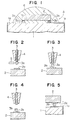
- a semiconductor device A is of a so-called flip-chip mount type constructed by disposing a semiconductor chip (semiconductor package) 2 in the central area of the upper surface of a substrate 1, electrically connecting the aluminium alloy wiring lines 2a, ie, wiring lines of an Al-Si alloy or an Al-Cu-Si alloy, of the semiconductor chip 2 to those of the wiring lines 1a, ie, Cu lines plated with Sn or Au, arranged on the upper surface of the substrate 1 with bump contacts 3b, and sealing the semiconductor chip 2 and part of the wiring lines 1a of the substrate 1 with a protective resin 6, such as a silicone resin.
- the bump contacts 3b are formed previously by bonding balls 3a formed by heating the tip of an alloy wire 3, ie, a connecting material, to the alloy wiring lines 2a of the semiconductor chip 2 through a procedure shown in Figs. 2 to 5.
- the alloy wire 3 is formed of an alloy consisting of Pb or Sn as a principal element, and additive elements and produced by a quench solidifying process.
- the alloy wire 3 may contain one or some additive elements among Be, B, C, Mg, Al, Si, P, Ca, Ti, V, Cr, Mn, Fe, Co, Ni, Cu, Zn, Ga, Ge, Se, Zr, Nb, Mo, Pd, Ag, Cd, Sb, Te, Ir, Pt, Au, Tl and Bi.
- An alloy not containing Pb or Sn as the principal element may contain Pb, Sn or In as an additive element.
- the alloy wire 3 thus produced is passed through a capillary tube 4, and then the tip of the alloy wire 3 is heated with an electric torch 5 to form a ball 3a having a hardness of H B 6 or higher. Then, as shown in Fig. 3, the capillary tube 4 is lowered to attach the ball 3a formed at the tip of the alloy wire 3 to the aluminium alloy wiring line 2a formed on the semiconductor chip 2.
- the ball 3a having a hardness of H B 6 or higher destroys an oxide film coating the surface of the aluminium alloy wiring line 2a having a hardness on the order of H B 12, and the ball 3a is bonded directly to the aluminium alloy wiring line 2a by the diffusion between the new surface of the ball 3a and the new surface of the aluminium alloy wiring line 2a. Subsequently, as shown in Fig. 4, the capillary 4 is raised to separate the ball 3a from the alloy wire 3 to leave the ball 3a as a bump contact 3b on the aluminium alloy wiring line 2a.
- the tip of the alloy wire 3 namely, the ball 3a is heated, the unequilibrated phase disappears and the crystal grains grow large in the junction of the alloy wire 3 and the ball 3a to reduce the tensile strength of the junction, so that the junction yields and breaks readily when the alloy wire 3 is raised by the capillary.
- semiconductor chip 2 is placed on the substrate 1 with the bump contacts 3b attached to the aluminium alloy wiring lines 2a in contact with the wiring lines 1a of the substrate 1, and then heat and pressure are applied to the bump contact 3b to connect electrically the aluminium alloy wiring lines 2a of the semiconductor chip 2 and the wiring lines 1a of the substrate and also to bond the semiconductor chip 2 to the substrate 1.
- the sphericity of the balls 3b can be improved by heating the balls 3b in the atmosphere of a flux of a chloride or an iodide before placing the balls 3b in contact with the wiring lines 1a of the substrate 1, the balls 3b may be attached to the wiring lines 1a without causing then to reflow.
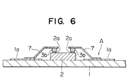
- Fig. 6 shows another semiconductor device A not forming part of the claimed invention.
- This semiconductor device A is of a so-called tape carrier bonding type, in which bump the contacts 3b are formed on the aluminium alloy wiring lines 2a of a semiconductor chip 2, and the film leads 7 formed for example, by plating strips of a Cu foil with Sn or Au, are bonded to the bump contacts 3b, and the wiring lines 1a of a substrate 1.
- the aluminium alloy wiring lines 2a are formed on the semiconductor chip 2 and the balls 3a are bonded to the aluminium alloy wiring lines 2a as the bump contacts 3b.
- the wiring lines 1a of the substrate 1 may be formed of an aluminium alloy and the balls 3a may be bonded to the wiring lines 1a of the substrate 1 as the bump contacts 3b.
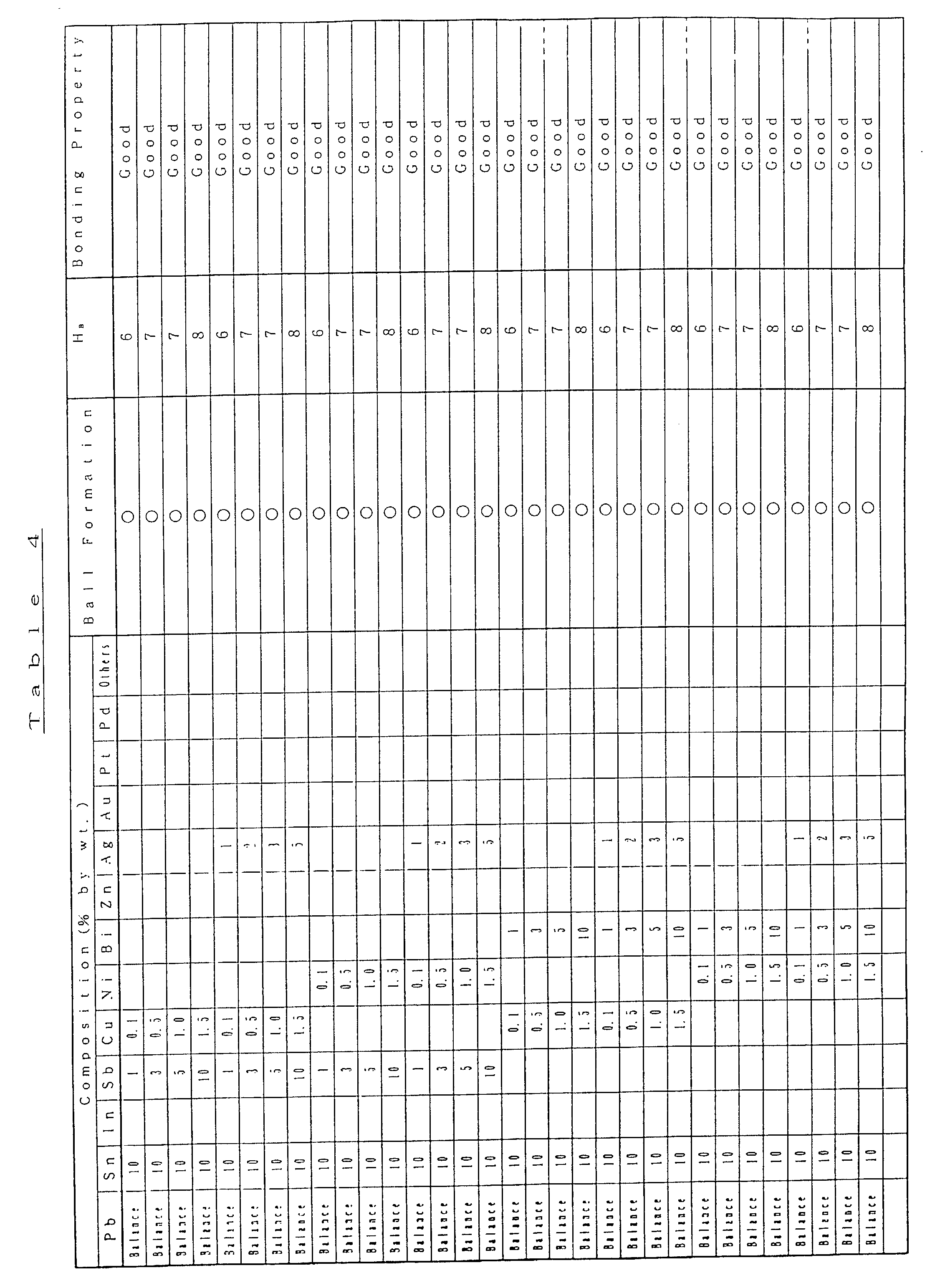
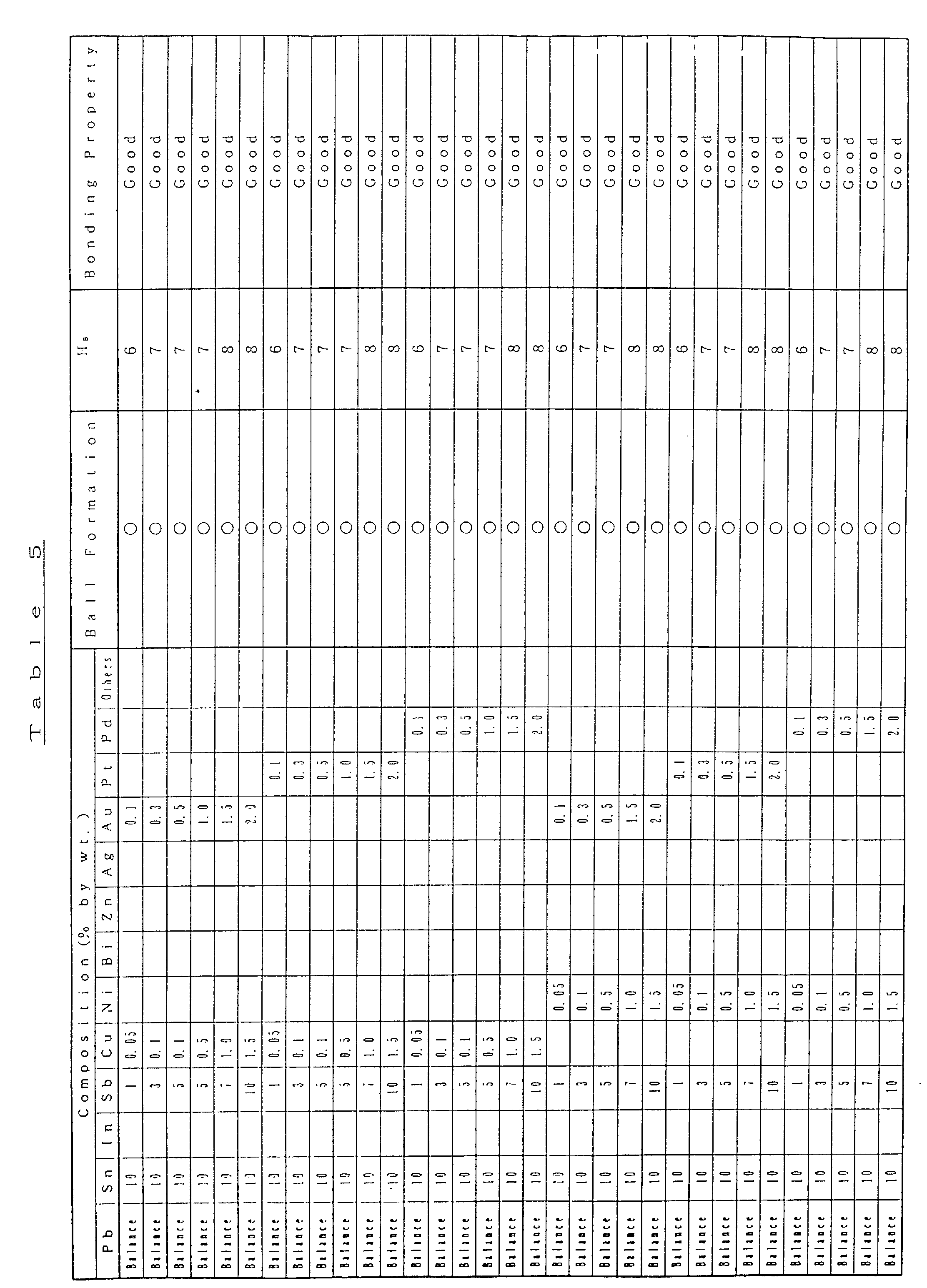
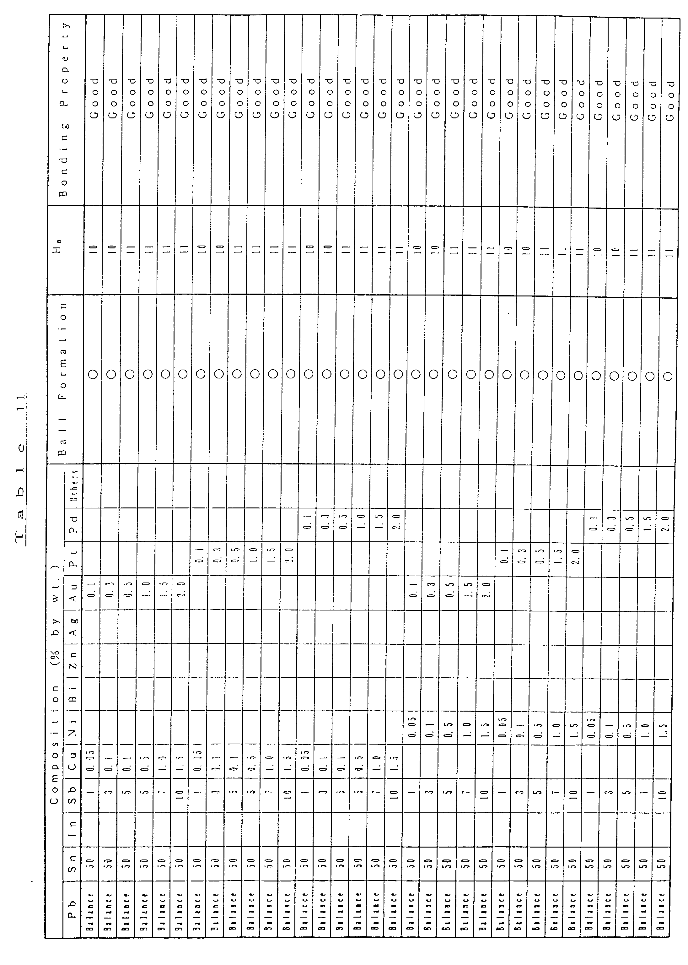
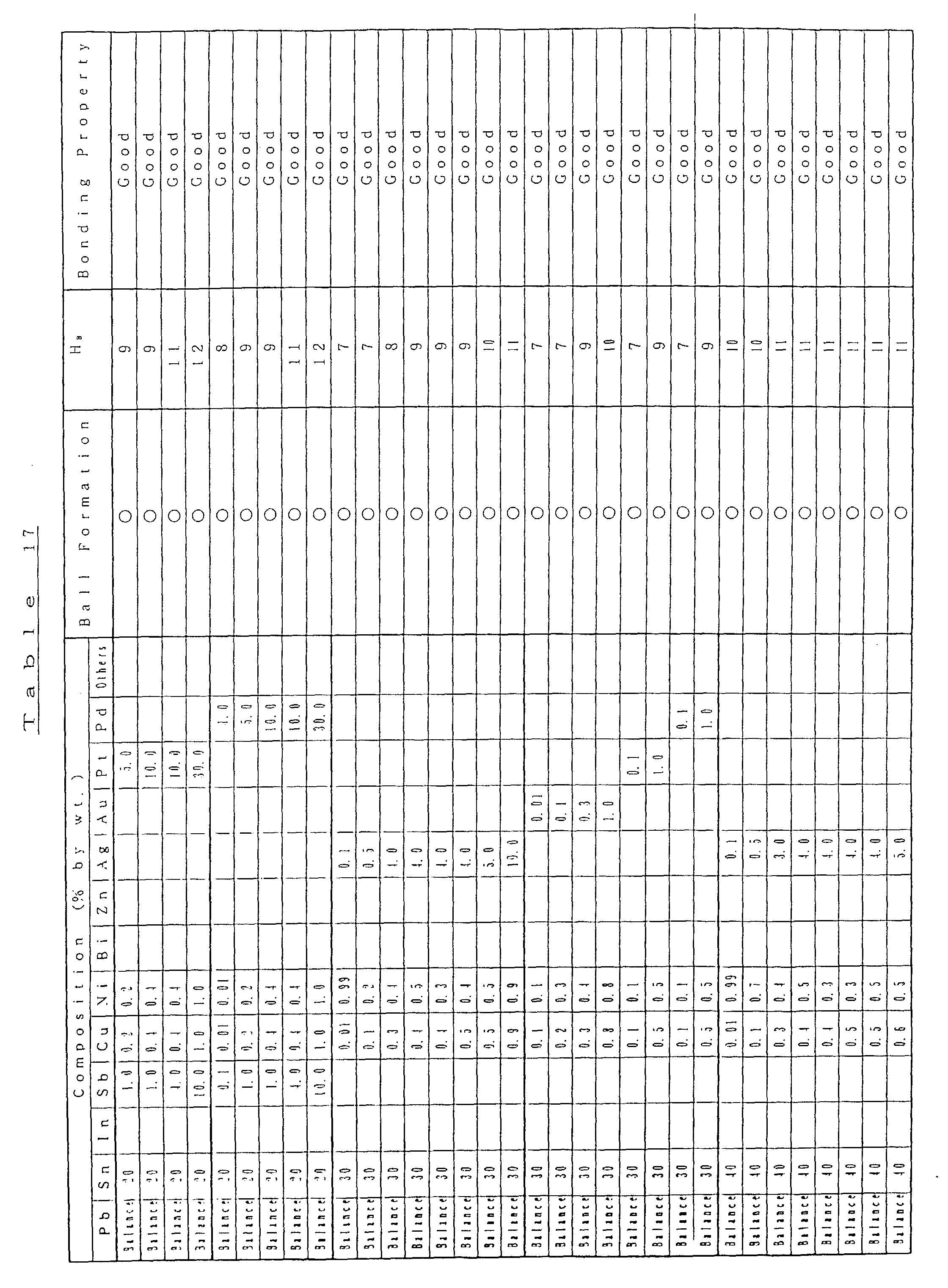
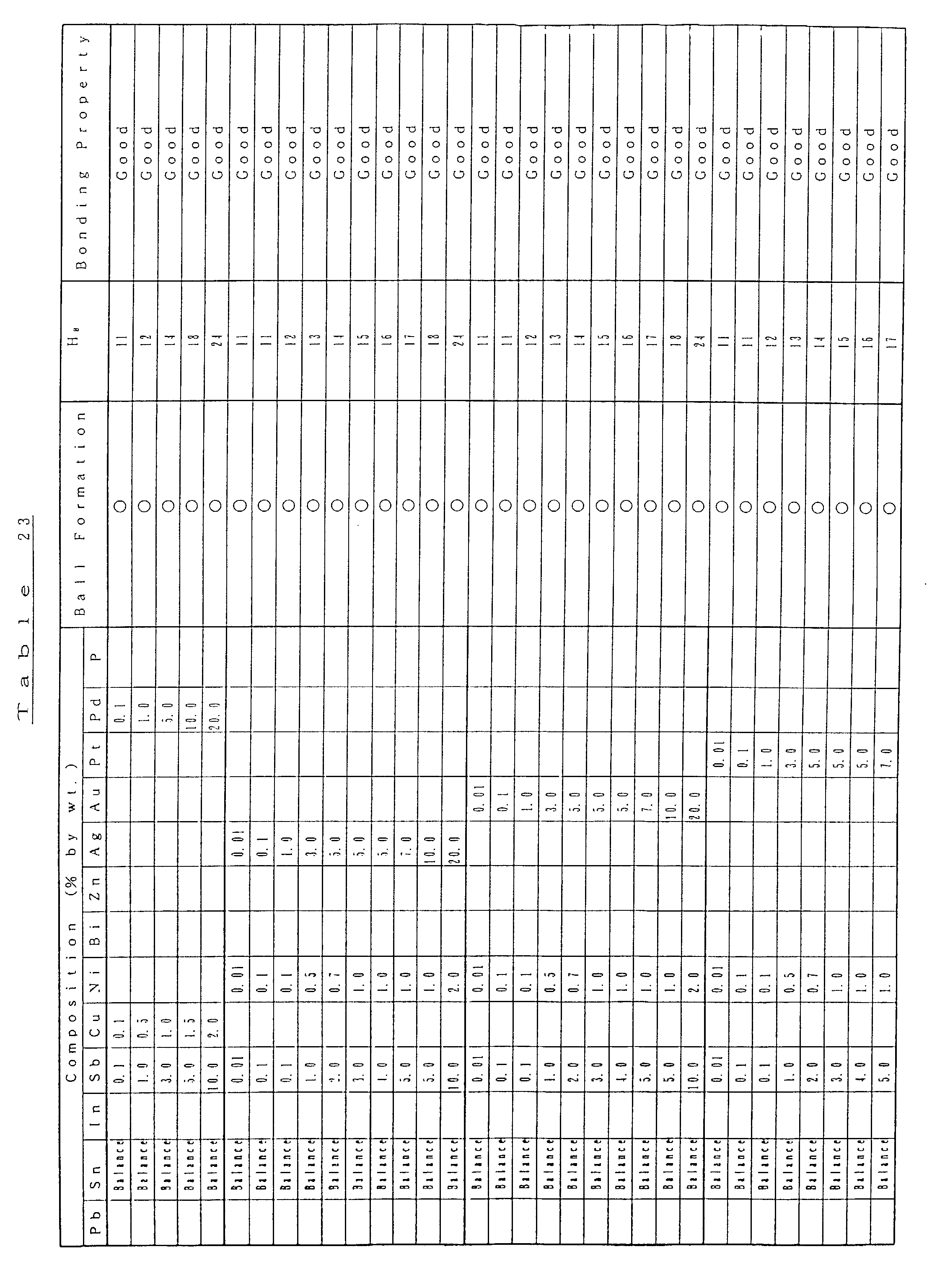
- Tables 1 to 27 show the properties of alloys in comparison with those of controls in terms of the respective compositions of alloys forming alloy wires, the ball forming property of the alloy wires, the hardness of balls formed by heating the alloy wires, and the capability of bonding to the Al-Si alloy wiring lines.
- the ball forming property is evaluated by the shape of a ball formed by arc discharge between the tip of a sample alloy wire passed through a ceramic capillary tube and an electrode disposed near the tip of the sample alloy wire in an argon gas atmosphere containing 5% in volume hydrogen gas.
- a circular mark indicates that the ball has satisfactory sphericity and smooth surface morphology.
- the present invention has the following advantages.
- the ball of a hardness of H B 6 or higher formed on the tip of the alloy wire produced by drawing a quench solidified alloy destroys an oxide film coating the surface of the aluminium alloy wiring line, and the ball and the aluminium alloy wiring line are bonded together metallurgically by mutual diffusion between the new surface of the aluminium alloy wiring line and the new surface of the ball, and hence the ball formed on the tip of the alloy wire can be directly joined as a bump contact to the aluminium alloy wiring line.
- the present invention enables the omission of a step of removing the oxide film coating the surface of the aluminium alloy wiring line, which reduces time and cost for assembling the semiconductor device.
Landscapes
- Engineering & Computer Science (AREA)
- Mechanical Engineering (AREA)
- Chemical & Material Sciences (AREA)
- Inorganic Chemistry (AREA)
- Wire Bonding (AREA)
- Electric Connection Of Electric Components To Printed Circuits (AREA)
- Peptides Or Proteins (AREA)
Description










Claims (7)
- A method for electrically connecting a semiconductor package to a substrate, said method comprising steps ofheating the tip of a drawn, quench solidified, fine alloy wire containing Pb or Sn as a principal element and including, when Pb is a principal element also 1-10 weight % Sb and 0.05-3% weight Zn, and when Sn is a principal element also 0.01-10% weight Sb and 0.01-10% weight Zn, to form a ball having a Brinell hardness number HB6, or higher,joining the ball to an oxide film covered aluminium alloy wiring line on the semiconductor package or the substrate to destroy the oxide film on the aluminium alloy wiring line and to metallurgically bond the ball directly to the aluminium alloy wiring line by the diffusion between the ball and the aluminium alloy wiring line, followed bypulling the alloy wire away from the semiconductor package or the substrate to separate the alloy wire from the ball and to leave the ball as a bump contact on the aluminium alloy wiring line of the semiconductor package or the substrate, andelectrically connecting the semiconductor package to the substrate through such bump contact.
- A semiconductor package connecting method according to Claim 1, wherein the alloy wire is passed through a capillary tube employed in a wire bonder, and the balls are joined to the aluminium alloy wiring lines by a wire bonding method.
- A semiconductor package connecting method according to Claim 1, wherein the alloy forming the alloy wire contains, as an additive element or additive elements one or some elements among Be, B, C, Mg, Al, Si, P, Ca, Ti, V, Cr, Mn, Fe, Co, Ni, Cu, Zn, Ga, Ge, Se, Zr, Nb, Mo, Pd, Ag, Cd, In, Sn, Pb, Sb, Te, Ir, Pt, Au and Bi.
- A semiconductor package connecting method according to Claim 1, wherein the Brinell hardness number of the ball is in the range of HB 6 to HB 26.
- A drawn, quench solidified, fine alloy, semiconductor package connecting wire capable, by being heated at its tip, of forming balls of a Brinell hardness number HB6 or higher to provide bump contacts for electrically connecting a semiconductor package to a substrate, wherein the fine alloy wire contains Pb or Sn as a principal element and also Sb and Zn in the following amounts:-a) when Pb is the principal element, 1-10 weight % Sb and 0.05-3 weight % Zn; andb) when Sn is the principal element, 1-10% weight Sb and 0.01-10 weight % Zn.
- A semiconductor package connecting wire according to Claim 5, wherein the alloy contains one or some elements among Be, B, C, Mg, Al, Si, P, Ca, Ti, V, Cr, Mn, Fe, Co, Ni, Cu, Zn, Ga, Ge, Se, Zr, Nb, Mo, Pd, Ag, Cd, In, Sn, Pb, Sb, Te, Ir, Pt, Au, Tl and Bi.
- A semiconductor package connecting wire according to Claim 5, wherein the Brinell hardness number of the ball is in the range of HB 6 to HB 26.
Applications Claiming Priority (6)
| Application Number | Priority Date | Filing Date | Title |
|---|---|---|---|
| JP34013289 | 1989-12-27 | ||
| JP340132/89 | 1989-12-27 | ||
| JP17199190 | 1990-06-29 | ||
| JP171991/90 | 1990-06-29 | ||
| JP22272990 | 1990-08-24 | ||
| JP222729/90 | 1990-08-24 |
Publications (3)
| Publication Number | Publication Date |
|---|---|
| EP0435009A2 EP0435009A2 (en) | 1991-07-03 |
| EP0435009A3 EP0435009A3 (en) | 1991-09-25 |
| EP0435009B1 true EP0435009B1 (en) | 1999-01-07 |
Family
ID=27323563
Family Applications (1)
| Application Number | Title | Priority Date | Filing Date |
|---|---|---|---|
| EP90122822A Expired - Lifetime EP0435009B1 (en) | 1989-12-27 | 1990-11-29 | Semiconductor package connecting method and semiconductor package connecting wires |
Country Status (7)
| Country | Link |
|---|---|
| US (2) | US5366692A (en) |
| EP (1) | EP0435009B1 (en) |
| JP (1) | JP2891432B2 (en) |
| AU (1) | AU643721B2 (en) |
| CA (1) | CA2031111A1 (en) |
| DE (1) | DE69032879T2 (en) |
| SG (1) | SG46506A1 (en) |
Families Citing this family (34)
| Publication number | Priority date | Publication date | Assignee | Title |
|---|---|---|---|---|
| GB2201545B (en) * | 1987-01-30 | 1991-09-11 | Tanaka Electronics Ind | Method for connecting semiconductor material |
| JP2891432B2 (en) * | 1989-12-27 | 1999-05-17 | 田中電子工業株式会社 | Connection method of semiconductor material, connection material used therefor, and semiconductor device |
| FR2696279B1 (en) * | 1992-09-25 | 1994-11-18 | Thomson Csf | Method for allowing the mounting of a chip on a substrate and chip prepared according to the method. |
| US5249732A (en) * | 1993-02-09 | 1993-10-05 | National Semiconductor Corp. | Method of bonding semiconductor chips to a substrate |
| JP3337049B2 (en) * | 1995-05-17 | 2002-10-21 | 田中電子工業株式会社 | Gold wire for bonding |
| US5985692A (en) * | 1995-06-07 | 1999-11-16 | Microunit Systems Engineering, Inc. | Process for flip-chip bonding a semiconductor die having gold bump electrodes |
| JP3238051B2 (en) * | 1995-08-25 | 2001-12-10 | 京セラ株式会社 | Brazing material |
| US6404063B2 (en) | 1995-12-22 | 2002-06-11 | Micron Technology, Inc. | Die-to-insert permanent connection and method of forming |
| US5776824A (en) * | 1995-12-22 | 1998-07-07 | Micron Technology, Inc. | Method for producing laminated film/metal structures for known good die ("KG") applications |
| US5686318A (en) * | 1995-12-22 | 1997-11-11 | Micron Technology, Inc. | Method of forming a die-to-insert permanent connection |
| US6371361B1 (en) * | 1996-02-09 | 2002-04-16 | Matsushita Electric Industrial Co., Ltd. | Soldering alloy, cream solder and soldering method |
| US5731244A (en) | 1996-05-28 | 1998-03-24 | Micron Technology, Inc. | Laser wire bonding for wire embedded dielectrics to integrated circuits |
| US5821494A (en) * | 1996-09-27 | 1998-10-13 | International Business Machines Corporation | Method of electrical connection between head transducer and suspension by solder wire bumping at slider level and laser reflow |
| JP3226213B2 (en) * | 1996-10-17 | 2001-11-05 | 松下電器産業株式会社 | Solder material and electronic component using the same |
| US6635514B1 (en) * | 1996-12-12 | 2003-10-21 | Tessera, Inc. | Compliant package with conductive elastomeric posts |
| US6179935B1 (en) * | 1997-04-16 | 2001-01-30 | Fuji Electric Co., Ltd. | Solder alloys |
| US5885893A (en) * | 1997-06-09 | 1999-03-23 | Highlight Optoelectronics, Inc. | Impact-free wire bonding of microelectronic devices |
| US6165888A (en) | 1997-10-02 | 2000-12-26 | Motorola, Inc. | Two step wire bond process |
| WO1999050901A1 (en) * | 1998-03-30 | 1999-10-07 | Yamatake Corporation | Soldering material for die bonding |
| JPH11340005A (en) * | 1998-05-28 | 1999-12-10 | Murata Mfg Co Ltd | Chip type electronic components |
| FR2786656B1 (en) * | 1998-11-27 | 2001-01-26 | Alstom Technology | ELECTRONIC POWER COMPONENT CONTAINING COOLING MEANS |
| JP3414342B2 (en) * | 1999-11-25 | 2003-06-09 | 日本電気株式会社 | Mounting structure and mounting method of integrated circuit chip |
| EP1243026A1 (en) * | 1999-12-21 | 2002-09-25 | Advanced Micro Devices, Inc. | Organic packages with solders for reliable flip chip connections |
| US20030001286A1 (en) * | 2000-01-28 | 2003-01-02 | Ryoichi Kajiwara | Semiconductor package and flip chip bonding method therein |
| JP4174174B2 (en) * | 2000-09-19 | 2008-10-29 | 株式会社ルネサステクノロジ | Semiconductor device, manufacturing method thereof, and semiconductor device mounting structure |
| US20030183948A1 (en) * | 2002-04-01 | 2003-10-02 | Tham Yew Fei | Golden unit |
| JP2005259915A (en) * | 2004-03-10 | 2005-09-22 | Nec Electronics Corp | Semiconductor device and manufacturing method thereof |
| US7749336B2 (en) | 2005-08-30 | 2010-07-06 | Indium Corporation Of America | Technique for increasing the compliance of tin-indium solders |
| US9260768B2 (en) * | 2005-12-13 | 2016-02-16 | Indium Corporation | Lead-free solder alloys and solder joints thereof with improved drop impact resistance |
| US8247272B2 (en) * | 2007-12-27 | 2012-08-21 | United Test And Assembly Center Ltd. | Copper on organic solderability preservative (OSP) interconnect and enhanced wire bonding process |
| DE102008054415A1 (en) * | 2008-12-09 | 2010-06-10 | Robert Bosch Gmbh | Arrangement of two substrates with a SLID bond connection and method for producing such an arrangement |
| EP2362432B1 (en) * | 2010-02-25 | 2017-06-07 | Saint-Augustin Canada Electric Inc. | Solar cell assembly |
| TWI395313B (en) | 2012-11-07 | 2013-05-01 | 樂金股份有限公司 | Solder ball bump structure and forming method thereof |
| JP2014151364A (en) * | 2013-02-13 | 2014-08-25 | Toyota Industries Corp | Solder and die bond structure |
Family Cites Families (24)
| Publication number | Priority date | Publication date | Assignee | Title |
|---|---|---|---|---|
| US2298237A (en) * | 1941-03-07 | 1942-10-06 | American Smelting Refining | Lead base coating alloy |
| US3644115A (en) * | 1970-03-23 | 1972-02-22 | Tatsuta Densen Kk | Soldering filler metal |
| US3744121A (en) * | 1970-08-15 | 1973-07-10 | Asahi Glass Co Ltd | Process for soldering difficultly solderable metals, such as si, ge, al, ti, zr and ta |
| US4106930A (en) * | 1972-02-19 | 1978-08-15 | Asahi Glass Company, Ltd. | Solder alloys for soldering difficultly solderable material |
| JPS54160525A (en) * | 1978-06-09 | 1979-12-19 | Sadaji Nagabori | Lead alloy for molten plating |
| US5223321A (en) * | 1981-07-17 | 1993-06-29 | British Telecommunications Plc | Tape-automated bonding of integrated circuits |
| US4588657A (en) * | 1984-11-01 | 1986-05-13 | Rca Corporation | Solder composition |
| US4622205A (en) * | 1985-04-12 | 1986-11-11 | Ibm Corporation | Electromigration lifetime increase of lead base alloys |
| US4670217A (en) * | 1985-07-26 | 1987-06-02 | J. W. Harris Company | Solder composition |
| US4654275A (en) * | 1985-11-27 | 1987-03-31 | Allied Corporation | Storage life of Pb-In-Ag solder foil by Sn addition |
| US4734256A (en) * | 1986-04-21 | 1988-03-29 | Allied-Signal Inc. | Wetting of low melting temperature solders by surface active additions |
| US5134460A (en) * | 1986-08-11 | 1992-07-28 | International Business Machines Corporation | Aluminum bump, reworkable bump, and titanium nitride structure for tab bonding |
| DE3785720T2 (en) * | 1986-09-25 | 1993-08-12 | Toshiba Kawasaki Kk | METHOD FOR PRODUCING A FILM CARRIER. |
| GB2201545B (en) * | 1987-01-30 | 1991-09-11 | Tanaka Electronics Ind | Method for connecting semiconductor material |
| JPS63301535A (en) * | 1987-01-30 | 1988-12-08 | Tanaka Electron Ind Co Ltd | Method for bonding semiconductor material and bonding material used therefor |
| EP0288776A3 (en) * | 1987-04-28 | 1989-03-22 | Texas Instruments Incorporated | Gold alloy wire connection to copper doped aluminum semiconductor circuit interconnection bonding pad |
| US4993622A (en) * | 1987-04-28 | 1991-02-19 | Texas Instruments Incorporated | Semiconductor integrated circuit chip interconnections and methods |
| US5019891A (en) * | 1988-01-20 | 1991-05-28 | Hitachi, Ltd. | Semiconductor device and method of fabricating the same |
| US4876221A (en) * | 1988-05-03 | 1989-10-24 | Matsushita Electric Industrial Co., Ltd. | Bonding method |
| US4950623A (en) * | 1988-08-02 | 1990-08-21 | Microelectronics Center Of North Carolina | Method of building solder bumps |
| US5066614A (en) * | 1988-11-21 | 1991-11-19 | Honeywell Inc. | Method of manufacturing a leadframe having conductive elements preformed with solder bumps |
| US5071787A (en) * | 1989-03-14 | 1991-12-10 | Kabushiki Kaisha Toshiba | Semiconductor device utilizing a face-down bonding and a method for manufacturing the same |
| US5011658A (en) * | 1989-05-31 | 1991-04-30 | International Business Machines Corporation | Copper doped low melt solder for component assembly and rework |
| JP2891432B2 (en) * | 1989-12-27 | 1999-05-17 | 田中電子工業株式会社 | Connection method of semiconductor material, connection material used therefor, and semiconductor device |
-
1990
- 1990-11-09 JP JP2304509A patent/JP2891432B2/en not_active Expired - Lifetime
- 1990-11-28 US US07/618,900 patent/US5366692A/en not_active Expired - Fee Related
- 1990-11-29 SG SG1996005329A patent/SG46506A1/en unknown
- 1990-11-29 CA CA002031111A patent/CA2031111A1/en not_active Abandoned
- 1990-11-29 EP EP90122822A patent/EP0435009B1/en not_active Expired - Lifetime
- 1990-11-29 DE DE69032879T patent/DE69032879T2/en not_active Expired - Fee Related
- 1990-12-17 AU AU68124/90A patent/AU643721B2/en not_active Ceased
-
1994
- 1994-07-29 US US08/282,020 patent/US5550407A/en not_active Expired - Fee Related
Non-Patent Citations (3)
| Title |
|---|
| Book no. , 1964, 'PHYSICAL METALLURGY PRINCIPLES', R. REED-HILL VAN NOSTRAND, U.S.A * |
| J.Japan Inst. Metals vo.58, no.8, 1994 pp.944-951 * |
| 'PHYSICAL METALLURGY PRINCIPLES',"R.Reed Hill","Van Nostrand","USA", 1994 * |
Also Published As
| Publication number | Publication date |
|---|---|
| EP0435009A3 (en) | 1991-09-25 |
| EP0435009A2 (en) | 1991-07-03 |
| US5366692A (en) | 1994-11-22 |
| CA2031111A1 (en) | 1991-06-28 |
| SG46506A1 (en) | 1998-02-20 |
| DE69032879T2 (en) | 1999-09-16 |
| JP2891432B2 (en) | 1999-05-17 |
| AU6812490A (en) | 1991-07-04 |
| AU643721B2 (en) | 1993-11-25 |
| US5550407A (en) | 1996-08-27 |
| JPH04174527A (en) | 1992-06-22 |
| DE69032879D1 (en) | 1999-02-18 |
Similar Documents
| Publication | Publication Date | Title |
|---|---|---|
| US5550407A (en) | Semiconductor device having an aluminum alloy wiring line | |
| KR100548114B1 (en) | Solder foil and semiconductor devices and electronic devices | |
| US7501337B2 (en) | Dual metal stud bumping for flip chip applications | |
| JP4051893B2 (en) | Electronics | |
| JP3736452B2 (en) | Solder foil | |
| JP2002124533A (en) | Electrode material, semiconductor device and mounting device | |
| US5249732A (en) | Method of bonding semiconductor chips to a substrate | |
| JP2737953B2 (en) | Gold alloy wire for gold bump | |
| JP4432541B2 (en) | Electronics | |
| JP2701419B2 (en) | Gold alloy fine wire for semiconductor element and bonding method thereof | |
| JP2007142271A (en) | Bump material and bonding structure | |
| JPS60134444A (en) | Formation for bump electrode | |
| JP2824302B2 (en) | Method of forming solder balls | |
| JP2911005B2 (en) | Processing method of bump electrode | |
| JP3142912B2 (en) | Solder material | |
| JP3091076B2 (en) | Small gold balls for bumps | |
| JP3086126B2 (en) | Small gold balls for bumps | |
| JPH07122564A (en) | Bump forming method | |
| JPH061779B2 (en) | Method for manufacturing semiconductor device | |
| JPH0465534B2 (en) | ||
| JP4335404B2 (en) | Electrode structure of electronic parts | |
| JPH07122562A (en) | Bump forming method, wire bonding method, bump structure, and wire bonding structure | |
| JPS63168031A (en) | Semiconductor device | |
| JPH0565052B2 (en) | ||
| JPH0565051B2 (en) |
Legal Events
| Date | Code | Title | Description |
|---|---|---|---|
| PUAI | Public reference made under article 153(3) epc to a published international application that has entered the european phase |
Free format text: ORIGINAL CODE: 0009012 |
|
| AK | Designated contracting states |
Kind code of ref document: A2 Designated state(s): DE FR GB NL SE |
|
| PUAL | Search report despatched |
Free format text: ORIGINAL CODE: 0009013 |
|
| AK | Designated contracting states |
Kind code of ref document: A3 Designated state(s): DE FR GB NL SE |
|
| RHK1 | Main classification (correction) |
Ipc: H01L 21/60 |
|
| 17P | Request for examination filed |
Effective date: 19911206 |
|
| 17Q | First examination report despatched |
Effective date: 19940725 |
|
| GRAG | Despatch of communication of intention to grant |
Free format text: ORIGINAL CODE: EPIDOS AGRA |
|
| GRAG | Despatch of communication of intention to grant |
Free format text: ORIGINAL CODE: EPIDOS AGRA |
|
| GRAH | Despatch of communication of intention to grant a patent |
Free format text: ORIGINAL CODE: EPIDOS IGRA |
|
| GRAH | Despatch of communication of intention to grant a patent |
Free format text: ORIGINAL CODE: EPIDOS IGRA |
|
| GRAA | (expected) grant |
Free format text: ORIGINAL CODE: 0009210 |
|
| AK | Designated contracting states |
Kind code of ref document: B1 Designated state(s): DE FR GB NL SE |
|
| PG25 | Lapsed in a contracting state [announced via postgrant information from national office to epo] |
Ref country code: SE Free format text: THE PATENT HAS BEEN ANNULLED BY A DECISION OF A NATIONAL AUTHORITY Effective date: 19990107 Ref country code: NL Free format text: LAPSE BECAUSE OF FAILURE TO SUBMIT A TRANSLATION OF THE DESCRIPTION OR TO PAY THE FEE WITHIN THE PRESCRIBED TIME-LIMIT Effective date: 19990107 Ref country code: FR Free format text: LAPSE BECAUSE OF FAILURE TO SUBMIT A TRANSLATION OF THE DESCRIPTION OR TO PAY THE FEE WITHIN THE PRESCRIBED TIME-LIMIT Effective date: 19990107 |
|
| REF | Corresponds to: |
Ref document number: 69032879 Country of ref document: DE Date of ref document: 19990218 |
|
| NLV1 | Nl: lapsed or annulled due to failure to fulfill the requirements of art. 29p and 29m of the patents act | ||
| EN | Fr: translation not filed | ||
| PLBE | No opposition filed within time limit |
Free format text: ORIGINAL CODE: 0009261 |
|
| STAA | Information on the status of an ep patent application or granted ep patent |
Free format text: STATUS: NO OPPOSITION FILED WITHIN TIME LIMIT |
|
| 26N | No opposition filed | ||
| PGFP | Annual fee paid to national office [announced via postgrant information from national office to epo] |
Ref country code: GB Payment date: 20001107 Year of fee payment: 11 |
|
| PGFP | Annual fee paid to national office [announced via postgrant information from national office to epo] |
Ref country code: DE Payment date: 20001127 Year of fee payment: 11 |
|
| PG25 | Lapsed in a contracting state [announced via postgrant information from national office to epo] |
Ref country code: GB Free format text: LAPSE BECAUSE OF NON-PAYMENT OF DUE FEES Effective date: 20011129 |
|
| REG | Reference to a national code |
Ref country code: GB Ref legal event code: IF02 |
|
| PG25 | Lapsed in a contracting state [announced via postgrant information from national office to epo] |
Ref country code: DE Free format text: LAPSE BECAUSE OF NON-PAYMENT OF DUE FEES Effective date: 20020702 |
|
| GBPC | Gb: european patent ceased through non-payment of renewal fee |
Effective date: 20011129 |