EP0432796A2 - Halbleiteranordnung - Google Patents
Halbleiteranordnung Download PDFInfo
- Publication number
- EP0432796A2 EP0432796A2 EP90124209A EP90124209A EP0432796A2 EP 0432796 A2 EP0432796 A2 EP 0432796A2 EP 90124209 A EP90124209 A EP 90124209A EP 90124209 A EP90124209 A EP 90124209A EP 0432796 A2 EP0432796 A2 EP 0432796A2
- Authority
- EP
- European Patent Office
- Prior art keywords
- area
- electrode
- external
- semiconductor device
- convex portion
- Prior art date
- Legal status (The legal status is an assumption and is not a legal conclusion. Google has not performed a legal analysis and makes no representation as to the accuracy of the status listed.)
- Granted
Links
Images




Classifications
-
- H—ELECTRICITY
- H10—SEMICONDUCTOR DEVICES; ELECTRIC SOLID-STATE DEVICES NOT OTHERWISE PROVIDED FOR
- H10W—GENERIC PACKAGES, INTERCONNECTIONS, CONNECTORS OR OTHER CONSTRUCTIONAL DETAILS OF DEVICES COVERED BY CLASS H10
- H10W72/00—Interconnections or connectors in packages
-
- H—ELECTRICITY
- H10—SEMICONDUCTOR DEVICES; ELECTRIC SOLID-STATE DEVICES NOT OTHERWISE PROVIDED FOR
- H10W—GENERIC PACKAGES, INTERCONNECTIONS, CONNECTORS OR OTHER CONSTRUCTIONAL DETAILS OF DEVICES COVERED BY CLASS H10
- H10W76/00—Containers; Fillings or auxiliary members therefor; Seals
- H10W76/10—Containers or parts thereof
- H10W76/12—Containers or parts thereof characterised by their shape
- H10W76/13—Containers comprising a conductive base serving as an interconnection
- H10W76/138—Containers comprising a conductive base serving as an interconnection having another interconnection being formed by a cover plate parallel to the conductive base, e.g. sandwich type
Definitions
- the present invention relates to a pressure contact type semiconductor device and an electrode block usable in the same, and more particularly, it relates to an improvement to homogenize a pressure distribution between an external electrode and a semiconductor substrate.
- an electrical contact of a semiconductor element with a control electrode conductor is kept by an elastic force of a spring, while external pressure is applied between an anode conductor and a cathode conductor provided in upper and lower portions of the semiconductor element.
- Fig. 9 is a sectional view showing a conventional pressure contact type gate turn-off thyristor (GTO).
- the flat pack type GTO 200 includes a semiconductor substrate 2, and the semiconductor substrate 2, has a pnpn 4-layer structure (not shown).
- a cathode electrode 10K and a gate electrode 10G made of aluminum are selectively formed.
- the cathode electrode 10K is positioned in the center portion of the upper major surface, while the gate electrode 10G is positioned around the same.
- an anode electrode 10A made of molybdenum and functioning also as a temperature compensating plate is brazed.
- a semiconductor element 1 is composed of the substrate 2 and the electrodes 10K, 10G and 10A.
- the anode electrode 10A is fitted into a guide ring 7, and this keeps the semiconductor element 1 in position.
- an external anode electrode 3 made of copper is disposed, while on an outer circumference of the external anode electrode 3 a flange 8b made of covar is brazed.
- Onto a lower lip of an insulating cylinder 5 made of ceramic another flange 8a is attached.
- the flanges 8a and 8b are brazed to each other to connect the insulating cylinder 5 with the external anode electrode 3.
- the insulating cylinder 5 is fitted on the guide ring 7.
- an external cathode electrode 20 made of copper is disposed at the upper portion of the semiconductor element 1.
- the external cathode electrode 20 has a convex portion 21 in the center part of its bottom surface, and the convex portion 21 is united with a circumferential portion 22.
- an annular groove (concave portion) 25 is formed in an area of the circumferential portion 22 adjacent to the convex portion 21, an annular groove (concave portion) 25 is formed.
- the convex portion 21 is in electrical contact with the cathode electrode 10K through the temperature compensating plate 11.
- the groove 25 is so positioned as to face the gate electrode 10G.
- an annular gate conductor 13 made of metal is disposed on the gate electrode 10G.
- the gate conductor 13 is electrically insulated from the external cathode electrode 20 by an insulating sheet 12.
- an insulating ring 44 and a flat washer 43 are disposed on the upper surface of the gate conductor 13.
- Another flat washer 41 is placed on the ceiling face of the groove 25, and a pair of conical springs 42 intervening between the flat washers 41 and 43 permit the gate conductor 13 to be in pressure contact with the gate electrode 10G (Fig. 9).
- a gate lead 6a made of silver is brazed to the gate conductor 13.
- the gate lead 6a is held in an insulating sleeve 6b and extends outwards from the insulating cylinder 5 through a bore formed in the wall of the insulating cylinder 5.
- the gate lead 6a is inserted into a tube 6c made of metal and welded to the tube 6c at its tip 6d. In this way, a gate electrode 6 is formed.
- a flange 4 is attached to an outer circumference of the external cathode electrode 20, and the flange 4 is brazed to an upper lip of the insulating cylinder 5 to connect the external cathode electrode 20 with the insulating cylinder 5.
- the GTO 200 When the GTO 200 having a structure as stated above is employed in an electric equipment, the GTO 200 should be positioned between an anode member 52 and a cathode member 51 of the equipment.
- the anode and cathode members 51 and 52 are pressed in a (-Z) direction and a (+Z) direction by springs, respectively, so that the bottom surface of the cathode member 51 is in press contact with an upper surface 23 of the external cathode electrode 20 while the upper surface of the anode member 52 is in press contact with a bottom surface 3a of the external anode electrode 3.
- the pressure force keeps the external cathode electrode 20 in electrical contact with the cathode electrode 10K through the temperature compensating board 11 and also keeps the external anode electrode 3 in electrical contact with the anode electrode 10A. Under such conditions, voltage is applied between the cathode member 51 and the anode member 52, and a gate signal is applied to the external gate electrode 6 so as to turn on or off the GTO 200.
- the external cathode electrode 20 and the external anode electrode 3 are so called stamp electrodes or post electrodes, and the surfaces 23 and 3a are post electrode faces.
- the external force partly applied to the convex portion 21 and the external cathode electrode 20 acts between the external cathode electrode 20 and the cathode electrode 10K.
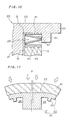
- the external force applied to a circumferential portion 22 of the external cathode electrode 20 does not act between the electrodes 20 and 10K but acts as a bending moment of the external cathode electrode 20 around a point S shown in Fig. 10. This is because there is no member for supporting the circumferential portion 22 from below, but merely an elastic force of the conical spring 42 acts upwards.
- the circumferential portion 22 of the external cathode electrode 20 is bent by an external force P applied from the cathode member 51 of the external equipment to the post electrode face 23. Accordingly, the shape of the groove 25 is deformed, and the pressure applied from the conical spring 42 (Fig. 10) held in the groove 25 to the gate conductor 13 is also changed. As a result, the pressure propagating from the gate conductor 13 to the semiconductor substrate 2 through the gate electrode 10G is changed, and there arises the disadvantage that a gate characteristic in the GTO 200 becomes unstable.
- the bending moment around the point S exerts effects on a stress distribution in the convex portion 21, and therefore, a spatial distribution of the pressure applied from the convex portion 21 to the cathode electrode 10K becomes uneven. Therefore, a contact resistance between the convex portion 21 and the cathode electrode 10K with the temperature compensating plate 11 intervening therebetween becomes spatially uneven, so that a current is concentrated in an area having a small contact resistance. This causes the semiconductor element 1 to locally generate larger heat while the GTO 200 is turning on, and there arises a problem that a thermal breakdown of the semiconductor element 1 is easily caused.
- the present invention is directed to a semiconductor device usable under the condition where an external force is applied thereto.
- the device comprises: (a) a semiconductor element having: (a-1) a semiconductor substrate having top and bottom major surfaces; (a-2) a first main electrode provided on a first region of the top major surface; (a-3) a control electrode provided on a second region of the top major surface, wherein the second region is separated from the first region in position; and (a-4) a second main electrode provided on the bottom major surface; (b) a first external main electrode member provided on the semiconductor element and comprising: (b-1) a bottom surface comprising a convex portion and a concave portion, wherein the convex portion is electrically in contact with the first main electrode and the concave portion is opposite to the control electrode across a gap; and (b-2) a top surface comprising a first area opposite to the convex portion and a second area at least a part of which is opposite to the concave portion, wherein a level of the first area is higher than a level of the second area; (c) control conductor inserted into
- the semiconductor device when an external force is applied to the top surface of the first external main electrode member, the external force acts on the first area of the top surface but not on the second area, because the second area is lower in level than the first area.
- the second area is opposite to at least a part of the concave portion of the bottom surface of the first external main electrode member, and hence a bending moment is substantially prevented from developing to the convex portion.
- the convex portion is not deformed, and no pressure charge is caused between the control conductor and the control electrode by the elastic force of the elastic member.
- any bending moment does not develop, a spatial uniformity of the pressure applied from the first area to the first main electrode in the semiconductor element can be maintained.
- the present invention is also directed to an electrode block made of a conductive material and usable in a semiconductor device, wherein the semiconductor device comprises a semiconductor substrate having a major surface on which first and second electrode layers are provided separately and wherein the electrode block is so placed on the major surface to be electrically in contact with the first electrode layer.
- the electrode block comprises: (a) a first surface having a convex portion and a concave portion whose respective positions on the first surface are so determined that the convex portion is electrically in contact with the first electrode layer and the concave portion is opposite to the second electrode layer across a gap when the electrode block is placed on the major surface of the semiconductor substrate; and (b) a second surface opposite to the first surface and having: (b-1) a first area opposite to the convex portion; and (b-2) a second area opposite to at least a part of the concave portion, wherein a level of the first area is higher than a level of the second area.
- the electrode block according to the present invention has a surface configuration usable as "the first external main electrode” in the above-mentioned semiconductor device.
- Fig. 1 is a sectional view showing a semiconductor device according to a preferred embodiment of the present invention
- Fig. 2 is a partial enlarged view of the semiconductor device shown in Fig. 1;
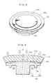
- Fig. 3 is a perspective view showing an electrode block employed as an external cathode electrode in the embodiment
- Fig. 4 is a diagram schematically showing the semiconductor device in Fig. 1 under the condition that an external force is applied thereto;
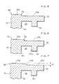
- Figs. 5 to 7 are partial enlarged sectional views showing other examples of the external cathode electrode
- Fig. 8 is an exploded sectional view showing a part of the semiconductor device according to another preferred embodiment of the present invention.
- Fig. 9 is a sectional view of a conventional semiconductor device
- Fig. 10 is a partial enlarged view of a semiconductor device in Fig. 9;
- Fig. 11 is a diagram schematically showing the semiconductor device in Fig. 9 to which external force is applied.
- Fig. 1 is a sectional view showing a GTO 100 according to a preferred embodiment of the present invention, where reference numerals are provided to corresponding components of the GTO 100 in Fig. 1 and the GTO 200 in Fig. 9.
- a component which is characteristic in the GTO 100 is an external cathode electrode 30, and details of the external cathode electrode 30 will be explained later.
- the external cathode electrode 30 is an electrode block formed of copper, including a cylindrical convex portion 31 and an annular groove (concave portion) 35 surrounding the convex portion 31. As shown in an enlarged view of Fig. 2, one of inner walls of the groove 35 is defined by an insulating sheet 12 covering a side surface 31a of the convex portion 31, while the other inner wall is defined by a surface 34a of an annular wall 34.
- the wall 34 is formed as a unity together with a circumferential portion 32 contiguous to the convex portion 31.
- An upper surface 33 of the external cathode electrode 30 has a 3-level step configuration.
- Fig. 2 shows an enlarged view of the step configuration
- Fig. 3 shows perspective view of the external cathode electrode 30.
- a first area 33a in the center portion is the highest
- a second area 33b surrounding the first area 33a is the second highest
- a third area 33c in the outermost part is the lowest.
- the difference ⁇ AH ab between the respective levels of the first and second areas 33a and 33b (Fig. 2) is approximately 1.0 mm
- the difference ⁇ H bc between the respective levels of the second and third areas 33b and 33c is approximately 0.5 mm.
- the areas 33a to 33c have their respective flat top surfaces.
- the first area 33a is opposed to a convex portion 31, while the second area 33b is opposed to the groove 35.
- the third area 33c is opposed to the wall 34 and a lower surface portion 36 extending from the same.
- the boundary B ab between the first and second areas 33a and 33b (Fig. 2) is aligned with the side surface 31a of the convex portion 31, while the boundary B bc between the second and third areas 33b and 33c is aligned with the side surface 34a of the wall 34.
- the first area 33a is circular in shape
- the second and thrid areas 33b and 33c are annular in shape.
- the external cathode electrode 30 can be obtained by cutting a cylindrical copper block.
- the GTO 100 when mounted in an external equipment, is inserted between the cathode member 51 and the anode member 52 (Fig. 1) of the external equipment.
- Surfaces 51a, 52a of the members 51 and 52 are flat, and therefore the surface 51a of the cathode member 51 comes in contact only with the first area 33a.
- the first area 33a corresponds to a post electrode surface of the external cathode electrode 30.
- the bottom surface 3a of the external anode electrode 3 is not formed as such a 3-level step configuration, and the entire bottom surface 3a functions as a post electrode face.
- the GTO 100 is used with a large pressure applied through the members 51 and 52.
- the member 51 itself is deformed in its outer circumferential portion, but the deformation is never propagated to the groove 35, because the second and third areas 33b and 33c are not in contact with the member 51.
- the urging force of the conical spring 42 to the gate conductor 13 in Fig. 2 is not changed, and a gate characteristic of the semiconductor element 1 keeps stable.
- the pressure distribution between the convex portion 31 and the cathode electrode 10K through the temperature compensating plate 11 is spatially uniform.
- a contact resistance in the interface between them is also spatially uniform, and any breakdown of the semiconductor element 1 is hardly caused by a generation of heat due to an uneven current distribution.
- the configuration of the external cathode electrode 30 is improved so that the troubles caused in the conventional GTO 200 can be effectively avoided.
- the upper surface 33 of the external cathode electrode 30 is formed not as a 2-level step configuration but as the 3-level step configuration for the following reason:
- the thickness of a region 37b (Fig. 2) between the groove 35 and the second area 33b considerably decreases.
- the region 37b is an important part to retain the strength and prevent the deformation around the groove 35, and hence, it is desirable to avoid excessive decrease in the thickness of the region 37b.
- the level of the second area 33b is not significantly low, and the level difference ⁇ H ab should be the lower limit or small enough to prevent the member 51 from coming into contact with the second area 33b.
- the third area 33c is lower in level than the second area 33b.
- the member 51 since the member 51 is deformed more because it is closer to its outer circumferential portion, it is especially effective for preventing the contact with the member 51 to make the third area 33c lower in level than the second area 33b.
- the 3-level step configuration of the preferred embodiment especially suits for an aspect of the present invention.
- An external cathode electrode 60 shown in a partial enlarged sectional view in Fig. 5 includes a circumferential portion 32 of which the entire top surface corresponds to the second area 33b.
- a deformation of the cathode member 51 of the external equipment is relatively small, such a 2-level step configuration also makes it possible to prevent the circumferential portion 32 from coming into contact with the cathode member 51. Also, even if the cathode member 51 is in contact with the circumferential portion 32 in some part, this results in a very little bending moment being applied to the circumferential portion 32.
- the boundary B ab between the first and second areas 33a and 33b is deviated from the position of the side face 31a of the convex portion 31, while the second area 33b is opposed to a part of the groove 35.
- the boundary B ab is desirably aligned with the side face 31a, but the modification as shown in Fig. 6 is also in the scope of the present invention.
- an area 63c lower than the first area 33a by a level difference ⁇ H lies around the first area 33a through a sloping face 63b.
- external cathode electrodes according to the present invention not only a step configuration but also a configuration including a slope are usable.
- Fig. 8 is a sectional view showing an external cathode electrode 90 of still another preferred embodiment.
- the external cathode electrode 90 is used as a combination with a semiconductor element 1a which is different in type from the semiconductor element 1 in Fig. 1.
- a cathode electrode 10K1 is provided in the center portion of the top surface of a semiconductor substrate 2 and additionally another cathode electrode 10K2 is provided on the outer side of the gate electrode 10G.
- an external cathode electrode 90 is configured as a unity which includes a convex portion 92 in the center portion and an annular outer circumferential portion 94 connected by a connecting portion 93.
- an annular groove 45 is formed, and insulating sheets 12 and 12a are attached to inner walls of the groove 45.
- a conical spring 42 is held in the groove 45, and an annular gate conductor 13 is urged downwards by the conical spring 42.
- an external gate electrode 6 inserted in a notch (not shown) formed in a part of the outer circumferential portion 94 is brazed to the gate conductor 13.
- the lower surfaces of the convex portion 92 and circumferential portion 94 are positioned opposite to the cathode electrodes 10K1 and 10K2 on the semiconductor substrate 2, while the lower surface of the gate conductor 13 is positioned opposite to the gate electrode 10G.
- the external cathode electrode 90 is mounted on the semiconductor element 1a as shown by an arrow of a broken line and comes into contact with the semiconductor element 1a by an external force.
- the external cathode electrode 90 of this type its upper surface 91 is formed as a step configuration composed of first to third areas 91a to 91c.
- the first area 91a is opposite to the convex portion 92, while the second area 91b is opposite to the groove 45.
- the third area 91c covers the top surface of the outer circumferential portion 94.
- the first and third areas 91a and 91c are at a same level, but the second area 91b is lower than them.
- the third area 91c is shaped to be able to come into contact with the cathode members of the external equipment, but the second area 91b only is not in contact with the cathode members.
- the present invention is applicable in various arrangtements of the cathode electrode and the gate electrode on the semiconductor substrate. Moreover, the present invention can be applied not only to GTOs but to all semiconductor devices having their respective control electrodes, such as other thyristors, transistors, etc.
Landscapes
- Thyristors (AREA)
- Die Bonding (AREA)
Applications Claiming Priority (2)
| Application Number | Priority Date | Filing Date | Title |
|---|---|---|---|
| JP326662/89 | 1989-12-15 | ||
| JP32666289A JPH0744191B2 (ja) | 1989-12-15 | 1989-12-15 | 半導体装置およびそのための電極ブロック |
Publications (3)
| Publication Number | Publication Date |
|---|---|
| EP0432796A2 true EP0432796A2 (de) | 1991-06-19 |
| EP0432796A3 EP0432796A3 (en) | 1991-09-11 |
| EP0432796B1 EP0432796B1 (de) | 1996-06-26 |
Family
ID=18190269
Family Applications (1)
| Application Number | Title | Priority Date | Filing Date |
|---|---|---|---|
| EP19900124209 Expired - Lifetime EP0432796B1 (de) | 1989-12-15 | 1990-12-14 | Halbleiteranordnung |
Country Status (4)
| Country | Link |
|---|---|
| US (1) | US5189509A (de) |
| EP (1) | EP0432796B1 (de) |
| JP (1) | JPH0744191B2 (de) |
| DE (1) | DE69027586T2 (de) |
Cited By (4)
| Publication number | Priority date | Publication date | Assignee | Title |
|---|---|---|---|---|
| EP0588026A3 (en) * | 1992-08-15 | 1994-09-07 | Abb Research Ltd | Turn-off high-power semiconductor device |
| US5539220A (en) * | 1993-07-27 | 1996-07-23 | Fuji Electric Co., Ltd. | Pressure contact semiconductor device in a flat package |
| US5786636A (en) * | 1993-09-29 | 1998-07-28 | Fuji Electric Co., Ltd. | Semiconductor device and method of fabricating same |
| US6624448B2 (en) * | 2000-09-28 | 2003-09-23 | Mitsubishi Denki Kabushiki Kaisha | Semiconductor device with multiple supporting points |
Families Citing this family (2)
| Publication number | Priority date | Publication date | Assignee | Title |
|---|---|---|---|---|
| JP3018971B2 (ja) * | 1995-12-18 | 2000-03-13 | 富士電機株式会社 | 半導体装置 |
| DE69626299T2 (de) * | 1996-09-24 | 2003-12-11 | Mitsubishi Denki K.K., Tokio/Tokyo | Halbleiteranordnung und verfahren zur herstellung |
Family Cites Families (10)
| Publication number | Priority date | Publication date | Assignee | Title |
|---|---|---|---|---|
| US3457472A (en) * | 1966-10-10 | 1969-07-22 | Gen Electric | Semiconductor devices adapted for pressure mounting |
| GB1133358A (en) * | 1966-11-11 | 1968-11-13 | Ass Elect Ind | Pressure contact semi-conductor devices |
| BE790502A (fr) * | 1971-10-26 | 1973-04-25 | Westinghouse Electric Corp | Dispositif semiconducteur encapsule a l'aide d'un elastomere |
| CH630490A5 (de) * | 1978-06-30 | 1982-06-15 | Bbc Brown Boveri & Cie | Gehaeuse fuer ein halbleiter-hochleistungsbauelement. |
| JPS5821347A (ja) * | 1981-07-29 | 1983-02-08 | Toshiba Corp | 平型半導体装置 |
| JPS5871633A (ja) * | 1981-10-23 | 1983-04-28 | Toshiba Corp | 圧接型半導体装置 |
| JPS58101433A (ja) * | 1981-12-11 | 1983-06-16 | Toshiba Corp | 加圧接触型半導体装置 |
| JPS6159742A (ja) * | 1984-08-30 | 1986-03-27 | Mitsubishi Electric Corp | 半導体装置 |
| JPS61208873A (ja) * | 1985-03-13 | 1986-09-17 | Res Dev Corp Of Japan | 圧接構造型両面ゲ−ト静電誘導サイリスタ |
| JPS61251043A (ja) * | 1985-04-30 | 1986-11-08 | Hitachi Ltd | 圧接型半導体装置 |
-
1989
- 1989-12-15 JP JP32666289A patent/JPH0744191B2/ja not_active Expired - Lifetime
-
1990
- 1990-12-04 US US07/621,967 patent/US5189509A/en not_active Expired - Fee Related
- 1990-12-14 DE DE69027586T patent/DE69027586T2/de not_active Expired - Fee Related
- 1990-12-14 EP EP19900124209 patent/EP0432796B1/de not_active Expired - Lifetime
Cited By (4)
| Publication number | Priority date | Publication date | Assignee | Title |
|---|---|---|---|---|
| EP0588026A3 (en) * | 1992-08-15 | 1994-09-07 | Abb Research Ltd | Turn-off high-power semiconductor device |
| US5539220A (en) * | 1993-07-27 | 1996-07-23 | Fuji Electric Co., Ltd. | Pressure contact semiconductor device in a flat package |
| US5786636A (en) * | 1993-09-29 | 1998-07-28 | Fuji Electric Co., Ltd. | Semiconductor device and method of fabricating same |
| US6624448B2 (en) * | 2000-09-28 | 2003-09-23 | Mitsubishi Denki Kabushiki Kaisha | Semiconductor device with multiple supporting points |
Also Published As
| Publication number | Publication date |
|---|---|
| DE69027586T2 (de) | 1997-02-06 |
| DE69027586D1 (de) | 1996-08-01 |
| EP0432796B1 (de) | 1996-06-26 |
| JPH03187235A (ja) | 1991-08-15 |
| EP0432796A3 (en) | 1991-09-11 |
| JPH0744191B2 (ja) | 1995-05-15 |
| US5189509A (en) | 1993-02-23 |
Similar Documents
| Publication | Publication Date | Title |
|---|---|---|
| US5001545A (en) | Formed top contact for non-flat semiconductor devices | |
| US5189509A (en) | Semiconductor device and electrode block for the same | |
| US6548890B2 (en) | Press-contact type semiconductor device | |
| JPH0760893B2 (ja) | 半導体装置およびその製造方法 | |
| EP0476661A2 (de) | Halbleiteranordnung vom Druckkontakttyp | |
| EP0158749A1 (de) | Halbleiteranordnung mit unter Druck stehenden Gliedern | |
| US4500907A (en) | Pressure-applied type semiconductor device | |
| US6445013B1 (en) | Gate commutated turn-off semiconductor device | |
| JPH08241956A (ja) | 半導体素子の圧力接触ハウジング | |
| EP0246574B1 (de) | Leistungshalbleiteranordnung | |
| US4556898A (en) | Semiconductor device | |
| US3457474A (en) | Semiconductor rectifier structure having semiconductor element assembly screwed into place on support base | |
| GB2038554A (en) | Thyristor | |
| US6465881B1 (en) | Compression bonded type semiconductor device | |
| US6339231B1 (en) | Gate commutated turn-off thyristor module | |
| EP0660396B1 (de) | MOS-Leistungs-Chip-Typ und Packungszusammenbau | |
| JPH0547991B2 (de) | ||
| EP1030355B1 (de) | Druckkontakt-halbleiteranordnung | |
| JP4125908B2 (ja) | 半導体装置 | |
| GB2052854A (en) | Semiconductor device with a low impedance base contact | |
| JP3334509B2 (ja) | 半導体装置 | |
| JP3161190B2 (ja) | 平型半導体装置 | |
| JPS5855648Y2 (ja) | 半導体装置 | |
| JPH04114474A (ja) | 半導体素子 | |
| JPH0328518Y2 (de) |
Legal Events
| Date | Code | Title | Description |
|---|---|---|---|
| PUAI | Public reference made under article 153(3) epc to a published international application that has entered the european phase |
Free format text: ORIGINAL CODE: 0009012 |
|
| 17P | Request for examination filed |
Effective date: 19901214 |
|
| AK | Designated contracting states |
Kind code of ref document: A2 Designated state(s): DE FR GB |
|
| PUAL | Search report despatched |
Free format text: ORIGINAL CODE: 0009013 |
|
| AK | Designated contracting states |
Kind code of ref document: A3 Designated state(s): DE FR GB |
|
| 17Q | First examination report despatched |
Effective date: 19931122 |
|
| GRAH | Despatch of communication of intention to grant a patent |
Free format text: ORIGINAL CODE: EPIDOS IGRA |
|
| GRAA | (expected) grant |
Free format text: ORIGINAL CODE: 0009210 |
|
| AK | Designated contracting states |
Kind code of ref document: B1 Designated state(s): DE FR GB |
|
| REF | Corresponds to: |
Ref document number: 69027586 Country of ref document: DE Date of ref document: 19960801 |
|
| REG | Reference to a national code |
Ref country code: GB Ref legal event code: 727 |
|
| REG | Reference to a national code |
Ref country code: GB Ref legal event code: 727A |
|
| ET | Fr: translation filed | ||
| REG | Reference to a national code |
Ref country code: GB Ref legal event code: 727B |
|
| REG | Reference to a national code |
Ref country code: GB Ref legal event code: SP |
|
| PLBE | No opposition filed within time limit |
Free format text: ORIGINAL CODE: 0009261 |
|
| STAA | Information on the status of an ep patent application or granted ep patent |
Free format text: STATUS: NO OPPOSITION FILED WITHIN TIME LIMIT |
|
| 26N | No opposition filed | ||
| REG | Reference to a national code |
Ref country code: GB Ref legal event code: 746 Effective date: 19990519 |
|
| REG | Reference to a national code |
Ref country code: FR Ref legal event code: D6 |
|
| PGFP | Annual fee paid to national office [announced via postgrant information from national office to epo] |
Ref country code: GB Payment date: 20011212 Year of fee payment: 12 Ref country code: FR Payment date: 20011212 Year of fee payment: 12 |
|
| REG | Reference to a national code |
Ref country code: GB Ref legal event code: IF02 |
|
| PG25 | Lapsed in a contracting state [announced via postgrant information from national office to epo] |
Ref country code: GB Free format text: LAPSE BECAUSE OF NON-PAYMENT OF DUE FEES Effective date: 20021214 |
|
| PGFP | Annual fee paid to national office [announced via postgrant information from national office to epo] |
Ref country code: DE Payment date: 20021219 Year of fee payment: 13 |
|
| GBPC | Gb: european patent ceased through non-payment of renewal fee |
Effective date: 20021214 |
|
| PG25 | Lapsed in a contracting state [announced via postgrant information from national office to epo] |
Ref country code: FR Free format text: LAPSE BECAUSE OF NON-PAYMENT OF DUE FEES Effective date: 20030901 |
|
| REG | Reference to a national code |
Ref country code: FR Ref legal event code: ST |
|
| PG25 | Lapsed in a contracting state [announced via postgrant information from national office to epo] |
Ref country code: DE Free format text: LAPSE BECAUSE OF NON-PAYMENT OF DUE FEES Effective date: 20040701 |