EP0431558A2 - Verfahren und Vorrichtung zur Herstellung eines Mehrelement-Dünnfilms mittels Ionenstrahlsputtern - Google Patents
Verfahren und Vorrichtung zur Herstellung eines Mehrelement-Dünnfilms mittels Ionenstrahlsputtern Download PDFInfo
- Publication number
- EP0431558A2 EP0431558A2 EP90123215A EP90123215A EP0431558A2 EP 0431558 A2 EP0431558 A2 EP 0431558A2 EP 90123215 A EP90123215 A EP 90123215A EP 90123215 A EP90123215 A EP 90123215A EP 0431558 A2 EP0431558 A2 EP 0431558A2
- Authority
- EP
- European Patent Office
- Prior art keywords
- ion beam
- substrate
- sputtered particles
- targets
- thin film
- Prior art date
- Legal status (The legal status is an assumption and is not a legal conclusion. Google has not performed a legal analysis and makes no representation as to the accuracy of the status listed.)
- Granted
Links
- 239000010409 thin film Substances 0.000 title claims abstract description 66
- 238000000034 method Methods 0.000 title claims description 51
- 238000001659 ion-beam spectroscopy Methods 0.000 title claims description 23
- 238000010884 ion-beam technique Methods 0.000 claims abstract description 92
- 239000000203 mixture Substances 0.000 claims abstract description 89
- 239000000758 substrate Substances 0.000 claims abstract description 55
- 239000002245 particle Substances 0.000 claims abstract description 54
- 238000005259 measurement Methods 0.000 claims abstract description 11
- 239000010408 film Substances 0.000 claims description 55
- 230000015572 biosynthetic process Effects 0.000 claims description 37
- 230000007935 neutral effect Effects 0.000 claims description 22
- 238000010521 absorption reaction Methods 0.000 claims description 20
- 238000004544 sputter deposition Methods 0.000 claims description 20
- IJGRMHOSHXDMSA-UHFFFAOYSA-N Atomic nitrogen Chemical compound N#N IJGRMHOSHXDMSA-UHFFFAOYSA-N 0.000 claims description 16
- QVGXLLKOCUKJST-UHFFFAOYSA-N atomic oxygen Chemical compound [O] QVGXLLKOCUKJST-UHFFFAOYSA-N 0.000 claims description 16
- 239000001301 oxygen Substances 0.000 claims description 16
- 229910052760 oxygen Inorganic materials 0.000 claims description 16
- 150000004767 nitrides Chemical class 0.000 claims description 12
- 239000000470 constituent Substances 0.000 claims description 10
- 239000000956 alloy Substances 0.000 claims description 9
- 229910045601 alloy Inorganic materials 0.000 claims description 9
- 239000002131 composite material Substances 0.000 claims description 9
- 238000001704 evaporation Methods 0.000 claims description 9
- 230000008020 evaporation Effects 0.000 claims description 9
- 229910044991 metal oxide Inorganic materials 0.000 claims description 8
- 230000001133 acceleration Effects 0.000 claims description 7
- 229910052757 nitrogen Inorganic materials 0.000 claims description 7
- 229910052751 metal Inorganic materials 0.000 claims description 6
- 239000002184 metal Substances 0.000 claims description 6
- 229910000765 intermetallic Inorganic materials 0.000 claims description 5
- 238000001514 detection method Methods 0.000 claims description 4
- 239000000463 material Substances 0.000 claims description 4
- 238000000151 deposition Methods 0.000 claims description 3
- 238000012358 sourcing Methods 0.000 claims 1
- 238000009826 distribution Methods 0.000 abstract description 3
- 150000001875 compounds Chemical class 0.000 description 11
- 239000010949 copper Substances 0.000 description 9
- XKRFYHLGVUSROY-UHFFFAOYSA-N Argon Chemical compound [Ar] XKRFYHLGVUSROY-UHFFFAOYSA-N 0.000 description 8
- 229910052782 aluminium Inorganic materials 0.000 description 8
- XAGFODPZIPBFFR-UHFFFAOYSA-N aluminium Chemical compound [Al] XAGFODPZIPBFFR-UHFFFAOYSA-N 0.000 description 8
- 238000012544 monitoring process Methods 0.000 description 7
- 239000013078 crystal Substances 0.000 description 6
- 238000002474 experimental method Methods 0.000 description 6
- RTAQQCXQSZGOHL-UHFFFAOYSA-N Titanium Chemical compound [Ti] RTAQQCXQSZGOHL-UHFFFAOYSA-N 0.000 description 5
- 229910052802 copper Inorganic materials 0.000 description 5
- 239000010936 titanium Substances 0.000 description 5
- 229910052719 titanium Inorganic materials 0.000 description 5
- OYPRJOBELJOOCE-UHFFFAOYSA-N Calcium Chemical compound [Ca] OYPRJOBELJOOCE-UHFFFAOYSA-N 0.000 description 4
- RYGMFSIKBFXOCR-UHFFFAOYSA-N Copper Chemical compound [Cu] RYGMFSIKBFXOCR-UHFFFAOYSA-N 0.000 description 4
- QPLDLSVMHZLSFG-UHFFFAOYSA-N Copper oxide Chemical compound [Cu]=O QPLDLSVMHZLSFG-UHFFFAOYSA-N 0.000 description 4
- 238000000137 annealing Methods 0.000 description 4
- 229910052786 argon Inorganic materials 0.000 description 4
- 229910052797 bismuth Inorganic materials 0.000 description 4
- 229910052791 calcium Inorganic materials 0.000 description 4
- 239000011575 calcium Substances 0.000 description 4
- 238000010894 electron beam technology Methods 0.000 description 4
- 238000010438 heat treatment Methods 0.000 description 4
- 238000011065 in-situ storage Methods 0.000 description 4
- 238000002128 reflection high energy electron diffraction Methods 0.000 description 4
- 229910052712 strontium Inorganic materials 0.000 description 4
- CIOAGBVUUVVLOB-UHFFFAOYSA-N strontium atom Chemical compound [Sr] CIOAGBVUUVVLOB-UHFFFAOYSA-N 0.000 description 4
- 239000005751 Copper oxide Substances 0.000 description 3
- CPLXHLVBOLITMK-UHFFFAOYSA-N Magnesium oxide Chemical compound [Mg]=O CPLXHLVBOLITMK-UHFFFAOYSA-N 0.000 description 3
- JCXGWMGPZLAOME-UHFFFAOYSA-N bismuth atom Chemical compound [Bi] JCXGWMGPZLAOME-UHFFFAOYSA-N 0.000 description 3
- 229910000431 copper oxide Inorganic materials 0.000 description 3
- 239000007789 gas Substances 0.000 description 3
- 239000012212 insulator Substances 0.000 description 3
- 150000002500 ions Chemical class 0.000 description 3
- 238000012545 processing Methods 0.000 description 3
- XUIMIQQOPSSXEZ-UHFFFAOYSA-N Silicon Chemical compound [Si] XUIMIQQOPSSXEZ-UHFFFAOYSA-N 0.000 description 2
- 229910000416 bismuth oxide Inorganic materials 0.000 description 2
- 230000008021 deposition Effects 0.000 description 2
- 238000010586 diagram Methods 0.000 description 2
- TYIXMATWDRGMPF-UHFFFAOYSA-N dibismuth;oxygen(2-) Chemical compound [O-2].[O-2].[O-2].[Bi+3].[Bi+3] TYIXMATWDRGMPF-UHFFFAOYSA-N 0.000 description 2
- 229910001873 dinitrogen Inorganic materials 0.000 description 2
- PCHJSUWPFVWCPO-UHFFFAOYSA-N gold Chemical compound [Au] PCHJSUWPFVWCPO-UHFFFAOYSA-N 0.000 description 2
- 229910052737 gold Inorganic materials 0.000 description 2
- 239000010931 gold Substances 0.000 description 2
- 239000007788 liquid Substances 0.000 description 2
- 239000000395 magnesium oxide Substances 0.000 description 2
- 229910052710 silicon Inorganic materials 0.000 description 2
- 239000010703 silicon Substances 0.000 description 2
- IATRAKWUXMZMIY-UHFFFAOYSA-N strontium oxide Chemical compound [O-2].[Sr+2] IATRAKWUXMZMIY-UHFFFAOYSA-N 0.000 description 2
- 239000000126 substance Substances 0.000 description 2
- 229910002480 Cu-O Inorganic materials 0.000 description 1
- 206010021143 Hypoxia Diseases 0.000 description 1
- NRTOMJZYCJJWKI-UHFFFAOYSA-N Titanium nitride Chemical compound [Ti]#N NRTOMJZYCJJWKI-UHFFFAOYSA-N 0.000 description 1
- 230000032683 aging Effects 0.000 description 1
- 238000004458 analytical method Methods 0.000 description 1
- 230000005540 biological transmission Effects 0.000 description 1
- BRPQOXSCLDDYGP-UHFFFAOYSA-N calcium oxide Chemical compound [O-2].[Ca+2] BRPQOXSCLDDYGP-UHFFFAOYSA-N 0.000 description 1
- ODINCKMPIJJUCX-UHFFFAOYSA-N calcium oxide Inorganic materials [Ca]=O ODINCKMPIJJUCX-UHFFFAOYSA-N 0.000 description 1
- 239000000292 calcium oxide Substances 0.000 description 1
- 230000003750 conditioning effect Effects 0.000 description 1
- 238000007796 conventional method Methods 0.000 description 1
- PMHQVHHXPFUNSP-UHFFFAOYSA-M copper(1+);methylsulfanylmethane;bromide Chemical compound Br[Cu].CSC PMHQVHHXPFUNSP-UHFFFAOYSA-M 0.000 description 1
- 238000012937 correction Methods 0.000 description 1
- 230000007812 deficiency Effects 0.000 description 1
- 238000011161 development Methods 0.000 description 1
- 230000018109 developmental process Effects 0.000 description 1
- 238000009792 diffusion process Methods 0.000 description 1
- 238000007599 discharging Methods 0.000 description 1
- 230000004927 fusion Effects 0.000 description 1
- 239000012535 impurity Substances 0.000 description 1
- 238000009413 insulation Methods 0.000 description 1
- 239000012774 insulation material Substances 0.000 description 1
- 238000004020 luminiscence type Methods 0.000 description 1
- AXZKOIWUVFPNLO-UHFFFAOYSA-N magnesium;oxygen(2-) Chemical compound [O-2].[Mg+2] AXZKOIWUVFPNLO-UHFFFAOYSA-N 0.000 description 1
- 239000007769 metal material Substances 0.000 description 1
- 229910021421 monocrystalline silicon Inorganic materials 0.000 description 1
- 230000003472 neutralizing effect Effects 0.000 description 1
- 230000003647 oxidation Effects 0.000 description 1
- 238000007254 oxidation reaction Methods 0.000 description 1
- 230000001737 promoting effect Effects 0.000 description 1
- 238000005086 pumping Methods 0.000 description 1
- 238000005546 reactive sputtering Methods 0.000 description 1
- 239000004065 semiconductor Substances 0.000 description 1
- 239000013077 target material Substances 0.000 description 1
- 238000009827 uniform distribution Methods 0.000 description 1
- 239000003039 volatile agent Substances 0.000 description 1
- XLYOFNOQVPJJNP-UHFFFAOYSA-N water Substances O XLYOFNOQVPJJNP-UHFFFAOYSA-N 0.000 description 1
Images


Classifications
-
- C—CHEMISTRY; METALLURGY
- C23—COATING METALLIC MATERIAL; COATING MATERIAL WITH METALLIC MATERIAL; CHEMICAL SURFACE TREATMENT; DIFFUSION TREATMENT OF METALLIC MATERIAL; COATING BY VACUUM EVAPORATION, BY SPUTTERING, BY ION IMPLANTATION OR BY CHEMICAL VAPOUR DEPOSITION, IN GENERAL; INHIBITING CORROSION OF METALLIC MATERIAL OR INCRUSTATION IN GENERAL
- C23C—COATING METALLIC MATERIAL; COATING MATERIAL WITH METALLIC MATERIAL; SURFACE TREATMENT OF METALLIC MATERIAL BY DIFFUSION INTO THE SURFACE, BY CHEMICAL CONVERSION OR SUBSTITUTION; COATING BY VACUUM EVAPORATION, BY SPUTTERING, BY ION IMPLANTATION OR BY CHEMICAL VAPOUR DEPOSITION, IN GENERAL
- C23C14/00—Coating by vacuum evaporation, by sputtering or by ion implantation of the coating forming material
- C23C14/22—Coating by vacuum evaporation, by sputtering or by ion implantation of the coating forming material characterised by the process of coating
- C23C14/54—Controlling or regulating the coating process
- C23C14/548—Controlling the composition
-
- C—CHEMISTRY; METALLURGY
- C23—COATING METALLIC MATERIAL; COATING MATERIAL WITH METALLIC MATERIAL; CHEMICAL SURFACE TREATMENT; DIFFUSION TREATMENT OF METALLIC MATERIAL; COATING BY VACUUM EVAPORATION, BY SPUTTERING, BY ION IMPLANTATION OR BY CHEMICAL VAPOUR DEPOSITION, IN GENERAL; INHIBITING CORROSION OF METALLIC MATERIAL OR INCRUSTATION IN GENERAL
- C23C—COATING METALLIC MATERIAL; COATING MATERIAL WITH METALLIC MATERIAL; SURFACE TREATMENT OF METALLIC MATERIAL BY DIFFUSION INTO THE SURFACE, BY CHEMICAL CONVERSION OR SUBSTITUTION; COATING BY VACUUM EVAPORATION, BY SPUTTERING, BY ION IMPLANTATION OR BY CHEMICAL VAPOUR DEPOSITION, IN GENERAL
- C23C14/00—Coating by vacuum evaporation, by sputtering or by ion implantation of the coating forming material
- C23C14/22—Coating by vacuum evaporation, by sputtering or by ion implantation of the coating forming material characterised by the process of coating
- C23C14/34—Sputtering
- C23C14/46—Sputtering by ion beam produced by an external ion source
Definitions
- the present invention relates to a method and apparatus for forming a multiple-element thin film based on ion beam sputtering.
- the composition control is determined from the relation between the quantity and condition of film formation on a try-and-error bais, and therefore if the surface condition or the like of the target changes or if the atmosphere of film formation changes when the experiment is put into practice, the sputtering rate and the rate of deposition on the substrate will vary, resulting in a deviated film composition.
- This problem is attributable to the absence of in-situ monitoring, i.e., on-the-spot observation, of the composition during the film formation, and the absence of a facility for conditioning the film formation based on the result of monitoring. Techniques related to this affair are described in JP-A-63-53265 and JP-A-63-241822, for example.
- An object of the present invention is to provide a method of thin film formation in accurate composition.
- Another object of the present invention is to provide a thin film forming apparatus capable of forming a thin film of accurate composition.
- This film forming method based on sputtering is capable of creating a high-performance thin film of both metallic and insulation materials at high adhesion easily and at high repeatability.
- the ion beam sputtering method which is distinct from the usual sputtering method in the formation a film in high vacuum on a substrate separated from plasma, has many superior features, such as that the film is insusceptible of damage from high-energy perticles, film formation parameters can be controlled independently, and inclusion of impurity in the film can be reduced.
- the ion beam sputtering method which is distinct from the usual sputtering method in the formation a film in high vacuum on a substrate separated from plasma, has many superior features, such as that the film is insusceptible of damage from high-energy perticles, film formation parameters can be controlled independently, and inclusion of impurity in the film can be reduced.
- high-temperature superconductive films, semiconductor thin film circuits, magnetic recording films, etc. there are demands of technical development for the creation of alloys
- the present invention is intended to enhance the accuracy of composition of a compound thin film which is formed of multiple elements, while exerting the advantages of the ion beam sputtering method and apparatus.
- the present invention is intended to overcome the foregoing problems, and its first object is to provide a method of forming a multiple-element thin film with a stable composition control property, in which each constituent can be controlled independently, the composition ratio of sputtered particles is monitored directly during the film formation, the ion beam sources or neutral beam sources are controlled dynamically based on the result of monitoring, and the film forming atmosphere can be treated as an independent condition, and its second object is to provide the apparatus which implements the above-mentioned method.
- the inventive method and apparatus are capable of controlling the concentration of each constituent accurately, and they are applicable favorably to the film formation of multiple-element compounds which need composition control, e.g., multiple-element oxides, multiple-element nitrides, multiple-element metallic compounds and alloys, gradient compounds, gradient alloys, and artificial super lattices.
- multiple-element compounds which need composition control, e.g., multiple-element oxides, multiple-element nitrides, multiple-element metallic compounds and alloys, gradient compounds, gradient alloys, and artificial super lattices.
- the above objective is namely to accomplish a film forming method and apparatus based on the simultaneous multiple-element ion beam sputtering, in which ion beam sources or neutral beam sources, at least equal in number to targets, are disposed and sputtered particles discharged from each target are deposited evenly at a controlled concentration on a substrate.
- the composition ratio of sputtered particles which pass by the substrate surface is measured by using the atomic absorption method, the measured data is rendered the computation process, and the acceleration voltage and the ion beam current density of each ion beam source are adjusted so as to achieve a proper composition ratio of sputtered particles thereby to control the concentration of sputtered particles.
- the ion beam sources use such rare gas as argon, or even oxygen or nitrogen depending on the composition of film.
- the beams of this type are charged electrostatically in general, and therefore in the case of targets made of insulator, e.g., oxide, the ion beams may be neutralized through a neutralizing filament before the beams are projected to the targets thereby to prevent the targets from being charged, when necessary.
- a constituent of the intended thin film composition includes an element which is gaseous or liquid at the room temperature, e.g., oxygen and water, it is also possible to feed the element together with an ion beam such as of argon directly to the intended thin film by means of the ion beam or neutral beam.
- an atomic absorption analyzing system For the means of measuring the concentration of sputtered particles, which are directed to the substrate, based on the atomic absorption method in the vicinity to the substrate, an atomic absorption analyzing system is used. Accordingly, the light transmitters and associated light receivers which constitute the detector of this system equal in number of sets to the number of kinds of sputtered particles that make the thin film, are disposed in the space between the targets and the substrate.
- the ion beams projected from the ion beam sources to the targets are converged so that about 99% or more of them are projected right on the targets, in order to attain the intended purity of the thin film. This enables the acceleration voltages and currents of the ion beam sources to be correspondent to the amount of sputter of target constituents, whereby the ion beam sputtering method and appartus with high composition controllability can be achieved.
- the scheme of atomic absorption method without the application of electron impingement or the like to sputtered particles is preferable, and through the dynamic control of each ion beam output based on the monitored information so that the intended composition is achieved, film formation which is insusceptible to the aging of target can be accomplished at high repeatability of composition.
- the compositions of ion beams or neutral beams for sputtering the targets and the compostions of sputtered prticles can be treated as independent film forming conditions.
- an ion beam source as an assistant ion beam source for projecting a low-energy ion beam or neutral beam of oxygen, nitrogen or the like to the substrate, it becomes possible to control the deficiency of oxide, nitride, etc., or to form a crystalline thin film with anisotropy in the crystal growing direction.
- the ion beam output for each target is controlled dynamically while conducting the in-situ monitoring of the composition of sputtered particles so that the composition of thin film can be controlled accurately, it is possible to form a compound thin film at high composition accuracy and high crystal property.
- the post annealing process can be eliminated, and it is possible to form a strong wiring without incurring a damage to the sharp slope of concentration at the junction.
- inventive method and apparatus of thin film formation in which the concentration of constituents can be controlled accurately, are suitable for the film formation of multiple-element compounds which necessitate the precise composition control, e.g., multiple-element oxides, multiple-element nitrides, multiple-element metallic compounds, alloys, gradient compounds, gradient alloys, and artificial super lattices.
- multiple-element oxides e.g., multiple-element oxides, multiple-element nitrides, multiple-element metallic compounds, alloys, gradient compounds, gradient alloys, and artificial super lattices.
- Fig. 1A is a front view of the apparatus which embodies the present invention.
- Fig. 1B is a plan view of the apparatus shown in Fig. 1A;
- Fig. 1C is a side view of the apparatus shown in Fig. 1A;
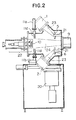
- Fig. 2 is a diagram showing the cross-section taken along the line IA-IA of Fig. 1A;
- Fig. 3 is a diagram explaining, in a sence of model, the overall apparatus based on the present invention.
- ion beam or neutral beam sources 1 through 4 for sputtering have corresponding four pieces of target 5 through 8 and an assistant ion beam source 9, as shown in Figs. 1 and 3.
- an atomic absorption analyzing system 11 Placed immediately in front of a film formation substrate 10 is an atomic absorption analyzing system 11 as shown in Figs. 2 and 3, which corresponds to four elements in this embodiment, and the analyzing system enables the monitoring of the composition of sputtered particles during the film formation.
- the substrate 10 is a monocrystalline MgO substrate, for example.
- blind tubes 11d attached to the ends of the system's light transmitter 11a and light receiver 11b so that the measurement open light path is confined to the proximity to the substrate thereby to shut out the unwanted stray light.
- the atomic absorption analyzing system 11 sends the resulting data to a data processing unit 17, as shown in Fig. 3, which implements the computation process and thereafter sends the resulting control data to power supplies 12-15 of the four ion beam sources 1-4 so that the outputs of ion beam sources are controlled in accordance with the prescribed compositions.
- the composition measurement based on the atomic absorption method can create error due to the output of the assistant ion beam source 9 and its chemical material, and in such event control data is sent to the power supply 16 of the assistant ion beam source 9 by being times to the atomic absorption measurement thereby to adjust the assistant ion beam output.
- a generally-known observation facility for the fast electron beam diffraction which includes a RHEED port 18, an RHEED electron gun 19, a cryopump 20 for the vacuum pumping system, a target manipulator 21 for varying the sputtering beam direction in response to the rotation and inclination of the target, and a substrate heating and turning system 22 for promoting the crystal formation, as shown in Figs. 1 and 2.
- the atomic absorption analyzing system 11 shown in Fig. 3 includes data output ports 11e and amplifiers 11f.
- the data processing unit 17 has a computation function, which calculates the deviations of concentration of sputtered particles from the predetermined values of composition and sends signals indicative of the detected differences to the power supplies 12-16 so that the ion beam sources are controlled on a feedback basis to produce proper beam outputs.
- Indicated by 25 is a display unit, on which information in the data processing unit 17, e.g., the preset values of composition, detected concentrations of sputtered particles, and beam correction outputs are displayed on a real time basis.
- the foregoing apparatus comprises four sets of ion beam sources, four pieces of target corresponding to the beam sources, an atomic absorption analyzing system for four elements, and an assistant ion beam source, the number of these functional components can of course be altered depending on the composition and structure of the thin film to be formed.
- the following embodiment is to form a film of Ba2YCu 3 O 7- ⁇ , which is one of the oxide high-temperature superconductive thin film, by using the ion beam sputtering apparatus based on the foregoing embodiment 1.
- the ion beam sources and targets were related as follows. Referring back to Fig. 3, the target 5 for the ion beam source 1 was a composite three-element sintered target of Ba-Cu-O for the Ba component, the target 6 for the ion beam source 2 was a Y2O 3 target for the Y component, and the targets 7 and 8 for the ion beam sources 3 and 4 were CuO or Cu targets for the Cu component.
- the target mount angle was adjusted so that all components were deposited in a uniform distribution on the substrate 10 where the thin film was formed. This adjustment is needed due to different flight angle distributions of sputtered particles discharged from the targets, resulting from differences in the thermal conductivity and beam energy needed for sputtering depending on each target material.
- An oxide superconductive thin film is apt to invite oxygen deficiency, and therefore the assistant ion beam or neutral beam source 9 is used to project an oxygen beam having energy up to 200 eV on to the growing thin film surface. Projection of oxygen beam ranging 50-100eV was most effective, yielding the intended oxide superconductive thin film of the above-mentioned composition.
- the critical temperature of superconduction of the film immediately after the film formation was 85°K.
- the temperature of substrate during the film formation was 450°C, and it exhibited superconductivity without the need of a post annealing process.
- the result of analysis revealed that the proportion of substances other than the superconductive material in the thin film was 1% or less in weight.
- the ion beam sources were operated at the following acceleration voltages and currents: Ion beam source 1: 1000 V, 100 mA; ion beam source 2: 700 V, 45 mA; ion beam sources 3 and 4: 700 V, 45 mA; assistant ion beam or neutral beam source 9: 100 V, 30 mA.
- the atomic absorption system has detection systems for elements of bismuth, strontium, calcium and copper.
- the apparatus was used for the film formation on a monocrystalline magnesium oxide substrate, which was being heated to 400°C.
- oxygen ion beam was used for the assistant ion.
- the resulting thin film satisfied the preset composition formula Bi2Sr2Ca2Cu3O X (where 5 ⁇ x ⁇ 10), and the critical temperature of superconduction was 95°K.
- the resulting thin film satisfied the preset composition formula Bi2Sr2Ca2Cu3O X (where 5 ⁇ x ⁇ 10), which was formed in a periodical fashion to complete a superconductive thin film of composite oxide in multi-layer structure, with composite oxides of different compositions being laminated alternately.
- the measurement of the superconductive characteristics of this thin film revealed the critical temperature of 100°K.
- Y-based Ba 2 YCu 3 O 7- ⁇ and Bi2Sr2Ca n-1 Cu n O 2n+2 are used as examples, the present invention is also applicable to high-temperature superconductive thin film of other types. Specifically, the invention can be applied to La-based La2 X Ba x CuO4, BPBO-based (Ba1 -X K X )BiO3, Tl-based Tl2Ba2Ca n-1 Cu n O 2n+2 , Pb-based Pb2Sr2ACu 3 O, Nb-based Nb2 X Ce X CuO4 Y ' and CaSr2(Cu, Bi)3O, for example.
- the following embodiment is to form a strong aluminum wiring on a monocrystalline silicon substrate by ion beam sputtering in the same manner as the embodiments 2 and 3 using the apparatus of the embodiment 1.
- Targets were each made of metallic titanium, aluminum, silicon and gold.
- a film of titanium is formed for about 50 ⁇ on a silicon substrate, and thereafter nitrogen gas is introduced gradually from the assistant ion beam source 9 so that a compositional slope from titanium layer to titanium nitride layer is formed continuously.
- the output of the ion beam source which sputters the aluminum target is raised gradually so that an intermediate layer made of titanium, aluminum and nitrogen is formed.
- the output of the ion beam source which sputters the titanium target is lowered gradually so that an insulation aluminum nitride layer is formed.
- the nitrogen gas assistant beam is halted so that a pure aluminum layer is formed by argon gas, sputtering.
- a thin film of gold is formed on the aluminum surface through the similar ion beam sputtering.
- the discontinuity of composition emerges at the interface of laminated thin films of different compositions, which apts to develop a peel-off.
- a post annealing process is conducted so that the diffusion takes place at each interface.
- the inventive method can readily form a continuous slope of composition, and high strength of adhesion can be achieved without the need of such post annealing process. Consequently, a strong aluminum wiring can be formed without incurring a damage to the junction interface having a sharp concentration profile.
Landscapes
- Chemical & Material Sciences (AREA)
- Chemical Kinetics & Catalysis (AREA)
- Engineering & Computer Science (AREA)
- Materials Engineering (AREA)
- Mechanical Engineering (AREA)
- Metallurgy (AREA)
- Organic Chemistry (AREA)
- Physical Vapour Deposition (AREA)
Applications Claiming Priority (2)
| Application Number | Priority Date | Filing Date | Title |
|---|---|---|---|
| JP313370/89 | 1989-12-04 | ||
| JP1313370A JP2713481B2 (ja) | 1989-12-04 | 1989-12-04 | イオンビームスパッタによる多元系薄膜形成方法および多元系薄膜形成装置 |
Publications (3)
| Publication Number | Publication Date |
|---|---|
| EP0431558A2 true EP0431558A2 (de) | 1991-06-12 |
| EP0431558A3 EP0431558A3 (en) | 1991-09-18 |
| EP0431558B1 EP0431558B1 (de) | 1995-04-12 |
Family
ID=18040443
Family Applications (1)
| Application Number | Title | Priority Date | Filing Date |
|---|---|---|---|
| EP90123215A Expired - Lifetime EP0431558B1 (de) | 1989-12-04 | 1990-12-04 | Verfahren und Vorrichtung zur Herstellung eines Mehrelement-Dünnfilms mittels Ionenstrahlsputtern |
Country Status (4)
| Country | Link |
|---|---|
| US (1) | US5089104A (de) |
| EP (1) | EP0431558B1 (de) |
| JP (1) | JP2713481B2 (de) |
| DE (1) | DE69018579T2 (de) |
Cited By (1)
| Publication number | Priority date | Publication date | Assignee | Title |
|---|---|---|---|---|
| US20200102644A1 (en) * | 2018-10-02 | 2020-04-02 | Korea Advanced Institute Of Science And Technology | Method of preparing multicomponent nanopattern |
Families Citing this family (35)
| Publication number | Priority date | Publication date | Assignee | Title |
|---|---|---|---|---|
| US5492605A (en) * | 1992-08-24 | 1996-02-20 | International Business Machines Corporation | Ion beam induced sputtered multilayered magnetic structures |
| US5364492A (en) * | 1992-09-17 | 1994-11-15 | Varian Associates, Inc. | Method of deposing by molecular beam epitaxy |
| JP3224293B2 (ja) * | 1992-12-01 | 2001-10-29 | 松下電器産業株式会社 | 誘電体薄膜の製造方法 |
| GB9225270D0 (en) * | 1992-12-03 | 1993-01-27 | Gec Ferranti Defence Syst | Depositing different materials on a substrate |
| JP3340803B2 (ja) * | 1993-06-25 | 2002-11-05 | 株式会社荏原製作所 | 高速原子ビームスパッタ成膜装置及び傾斜機能薄膜の製造方法 |
| JP3308135B2 (ja) * | 1994-11-01 | 2002-07-29 | 松下電器産業株式会社 | インプロセス膜厚モニター装置及び方法 |
| JPH08296042A (ja) * | 1995-04-17 | 1996-11-12 | Read Rite Corp | 複数イオンビームによる絶縁薄膜の形成方法 |
| US6224718B1 (en) | 1999-07-14 | 2001-05-01 | Veeco Instruments, Inc. | Target assembly for ion beam sputter deposition with multiple paddles each having targets on both sides |
| DE60135100D1 (de) * | 2000-03-24 | 2008-09-11 | Cymbet Corp | E mit ultradünnem elektrolyten |
| US6610352B2 (en) * | 2000-12-22 | 2003-08-26 | Ifire Technology, Inc. | Multiple source deposition process |
| US6402900B1 (en) | 2001-03-16 | 2002-06-11 | 4 Wave, Inc. | System and method for performing sputter deposition using ion sources, targets and a substrate arranged about the faces of a cube |
| US6679976B2 (en) | 2001-03-16 | 2004-01-20 | 4Wave, Inc. | System and method for performing sputter deposition with multiple targets using independent ion and electron sources and independent target biasing with DC pulse signals |
| DE10120383B4 (de) * | 2001-04-25 | 2007-07-26 | X-Fab Semiconductor Foundries Ag | Verfahren zur Metallisierung von Siliziumscheiben durch Aufsputtern |
| GB0127251D0 (en) * | 2001-11-13 | 2002-01-02 | Nordiko Ltd | Apparatus |
| JP2003158308A (ja) * | 2001-11-22 | 2003-05-30 | Communication Research Laboratory | 超伝導材料の製造方法 |
| US6906436B2 (en) * | 2003-01-02 | 2005-06-14 | Cymbet Corporation | Solid state activity-activated battery device and method |
| US7603144B2 (en) * | 2003-01-02 | 2009-10-13 | Cymbet Corporation | Active wireless tagging system on peel and stick substrate |
| US7294209B2 (en) * | 2003-01-02 | 2007-11-13 | Cymbet Corporation | Apparatus and method for depositing material onto a substrate using a roll-to-roll mask |
| US20040131760A1 (en) * | 2003-01-02 | 2004-07-08 | Stuart Shakespeare | Apparatus and method for depositing material onto multiple independently moving substrates in a chamber |
| US7211351B2 (en) | 2003-10-16 | 2007-05-01 | Cymbet Corporation | Lithium/air batteries with LiPON as separator and protective barrier and method |
| JP2007518246A (ja) * | 2004-01-06 | 2007-07-05 | シンベット コーポーレーション | 境界を有する1若しくはそれ以上の層を備える層状のバリア構造及び該バリア構造の製造方法 |
| US20070012244A1 (en) * | 2005-07-15 | 2007-01-18 | Cymbet Corporation | Apparatus and method for making thin-film batteries with soft and hard electrolyte layers |
| US7776478B2 (en) * | 2005-07-15 | 2010-08-17 | Cymbet Corporation | Thin-film batteries with polymer and LiPON electrolyte layers and method |
| KR101387855B1 (ko) * | 2005-07-15 | 2014-04-22 | 사임베트 코퍼레이션 | 연질 및 경질 전해질층을 가진 박막 배터리 및 그 제조방법 |
| JP4162094B2 (ja) * | 2006-05-30 | 2008-10-08 | 三菱重工業株式会社 | 常温接合によるデバイス、デバイス製造方法ならびに常温接合装置 |
| JP4172806B2 (ja) * | 2006-09-06 | 2008-10-29 | 三菱重工業株式会社 | 常温接合方法及び常温接合装置 |
| WO2011043407A1 (ja) * | 2009-10-08 | 2011-04-14 | 株式会社フジクラ | イオンビームアシストスパッタ装置及びイオンビームアシストスパッタ方法 |
| US11527774B2 (en) | 2011-06-29 | 2022-12-13 | Space Charge, LLC | Electrochemical energy storage devices |
| US9853325B2 (en) | 2011-06-29 | 2017-12-26 | Space Charge, LLC | Rugged, gel-free, lithium-free, high energy density solid-state electrochemical energy storage devices |
| US10601074B2 (en) | 2011-06-29 | 2020-03-24 | Space Charge, LLC | Rugged, gel-free, lithium-free, high energy density solid-state electrochemical energy storage devices |
| US10658705B2 (en) | 2018-03-07 | 2020-05-19 | Space Charge, LLC | Thin-film solid-state energy storage devices |
| US11996517B2 (en) | 2011-06-29 | 2024-05-28 | Space Charge, LLC | Electrochemical energy storage devices |
| US9988711B2 (en) * | 2015-05-14 | 2018-06-05 | Varian Semiconductor Equipment Associates, Inc. | Apparatus and method for multilayer deposition |
| JP2017057487A (ja) * | 2015-09-18 | 2017-03-23 | 日本放送協会 | イオンビームスパッタ装置 |
| CN114774846A (zh) * | 2022-04-14 | 2022-07-22 | 中建材玻璃新材料研究院集团有限公司 | 一种n掺杂c膜的制备方法 |
Family Cites Families (9)
| Publication number | Priority date | Publication date | Assignee | Title |
|---|---|---|---|---|
| US3734620A (en) * | 1971-04-01 | 1973-05-22 | Ibm | Multiple band atomic absorption apparatus for simultaneously measuring different physical parameters of a material |
| JPS57161063A (en) * | 1981-03-31 | 1982-10-04 | Nippon Sheet Glass Co Ltd | Method and device for sticking metallic oxide film on substrate |
| US4637869A (en) * | 1984-09-04 | 1987-01-20 | The Standard Oil Company | Dual ion beam deposition of amorphous semiconductor films |
| US4673475A (en) * | 1985-06-28 | 1987-06-16 | The Standard Oil Company | Dual ion beam deposition of dense films |
| DE3625700A1 (de) * | 1986-07-30 | 1988-02-04 | Siemens Ag | Einrichtung zur herstellung und analyse von mehrkomoponentenfilmen |
| US4793908A (en) * | 1986-12-29 | 1988-12-27 | Rockwell International Corporation | Multiple ion source method and apparatus for fabricating multilayer optical films |
| DE3709177A1 (de) * | 1987-03-20 | 1988-09-29 | Leybold Ag | Verfahren und vorrichtung zur regelung der reaktiven schichtabscheidung auf substraten mittels magnetronkatoden |
| JPH01108378A (ja) * | 1987-10-21 | 1989-04-25 | Mitsubishi Electric Corp | スパツタ装置 |
| JPH02217468A (ja) * | 1989-02-20 | 1990-08-30 | Olympus Optical Co Ltd | 化合物薄膜形成装置 |
-
1989
- 1989-12-04 JP JP1313370A patent/JP2713481B2/ja not_active Expired - Fee Related
-
1990
- 1990-12-03 US US07/620,611 patent/US5089104A/en not_active Expired - Lifetime
- 1990-12-04 EP EP90123215A patent/EP0431558B1/de not_active Expired - Lifetime
- 1990-12-04 DE DE69018579T patent/DE69018579T2/de not_active Expired - Fee Related
Cited By (2)
| Publication number | Priority date | Publication date | Assignee | Title |
|---|---|---|---|---|
| US20200102644A1 (en) * | 2018-10-02 | 2020-04-02 | Korea Advanced Institute Of Science And Technology | Method of preparing multicomponent nanopattern |
| US12378661B2 (en) * | 2018-10-02 | 2025-08-05 | Korea Advanced Institute Of Science And Technology | Method of preparing multicomponent nanopattern |
Also Published As
| Publication number | Publication date |
|---|---|
| JP2713481B2 (ja) | 1998-02-16 |
| EP0431558A3 (en) | 1991-09-18 |
| US5089104A (en) | 1992-02-18 |
| EP0431558B1 (de) | 1995-04-12 |
| DE69018579T2 (de) | 1995-09-07 |
| DE69018579D1 (de) | 1995-05-18 |
| JPH03173770A (ja) | 1991-07-29 |
Similar Documents
| Publication | Publication Date | Title |
|---|---|---|
| EP0431558B1 (de) | Verfahren und Vorrichtung zur Herstellung eines Mehrelement-Dünnfilms mittels Ionenstrahlsputtern | |
| Harper et al. | Synthesis of compound thin films by dual ion beam deposition. I. Experimental approach | |
| US5439575A (en) | Hybrid method for depositing semi-conductive materials | |
| EP0291044B1 (de) | Verfahren und Vorrichtung eines dünnen Films mit einer grossen Oberfläche durch Zerstäubung aus einer Verbindung | |
| Selinder et al. | Resputtering effects on the stoichiometry of YBa2Cu3O x thin films | |
| US5057201A (en) | Process for depositing a superconducting thin film | |
| Senthil Nathan et al. | Transport of sputtered atoms in facing targets sputtering geometry: A numerical simulation study | |
| Kwok | Formation of atomic beams and dynamics of in situ superconducting film growth by pulsed-laser deposition | |
| Raven | Radio frequency sputtering and the deposition of high-temperature superconductors | |
| US4882023A (en) | Method and system for producing thin films | |
| Jones et al. | Some superconducting and normal state properties of niobium nitride thin films | |
| US5679625A (en) | Method of making an oxide superconducting thin film | |
| Meyer et al. | Validity of Bragg's rule in sputtered superconducting NbN and NbC films of various compositions | |
| JPH05116940A (ja) | 基板上に金属酸化物の薄膜を生成させる方法 | |
| Sevenhans et al. | Mass spectrometer controlled electron beam evaporation synthesis of multilayered materials | |
| Booi et al. | Intrinsic stress in dc sputtered niobium | |
| Michel et al. | The preparation of YBCO thin films by a four ion beam co-deposition system | |
| Vandenberg et al. | Structural aspects of tunnel‐junction coupled granular lead films | |
| Truman et al. | Continued improvement of large area, in situ sputter deposition of superconducting YBCO thin films | |
| EP0487421A2 (de) | Verfahren zum Herstellen einer Dünnschicht aus oxydisch supraleitendem Bismuth-Typ | |
| JP2976382B2 (ja) | スパッタリング方法及びスパッタリング装置 | |
| Quigley et al. | Time dependence and spatial distribution of the deposition rate of YBa 2 Cu 3 O 7 thin films in 90° off-axis sputtering | |
| Koprio et al. | Quadrupole mass spectrometer monitored and controlled thin film deposition processes under ultrahigh vacuum conditions | |
| Shah et al. | Growth and properties of YBa2Cu3O7− x superconducting thin films | |
| MICHEL et al. | Institute of Micro-and Optoelectronics, Department of Physics, Swiss Federal Institute |
Legal Events
| Date | Code | Title | Description |
|---|---|---|---|
| PUAI | Public reference made under article 153(3) epc to a published international application that has entered the european phase |
Free format text: ORIGINAL CODE: 0009012 |
|
| 17P | Request for examination filed |
Effective date: 19901204 |
|
| AK | Designated contracting states |
Kind code of ref document: A2 Designated state(s): DE FR GB |
|
| PUAL | Search report despatched |
Free format text: ORIGINAL CODE: 0009013 |
|
| AK | Designated contracting states |
Kind code of ref document: A3 Designated state(s): DE FR GB |
|
| 17Q | First examination report despatched |
Effective date: 19930624 |
|
| GRAA | (expected) grant |
Free format text: ORIGINAL CODE: 0009210 |
|
| AK | Designated contracting states |
Kind code of ref document: B1 Designated state(s): DE FR GB |
|
| REF | Corresponds to: |
Ref document number: 69018579 Country of ref document: DE Date of ref document: 19950518 |
|
| ET | Fr: translation filed | ||
| PLBE | No opposition filed within time limit |
Free format text: ORIGINAL CODE: 0009261 |
|
| STAA | Information on the status of an ep patent application or granted ep patent |
Free format text: STATUS: NO OPPOSITION FILED WITHIN TIME LIMIT |
|
| 26N | No opposition filed | ||
| REG | Reference to a national code |
Ref country code: GB Ref legal event code: IF02 |
|
| PGFP | Annual fee paid to national office [announced via postgrant information from national office to epo] |
Ref country code: FR Payment date: 20031124 Year of fee payment: 14 |
|
| PGFP | Annual fee paid to national office [announced via postgrant information from national office to epo] |
Ref country code: GB Payment date: 20031126 Year of fee payment: 14 |
|
| PGFP | Annual fee paid to national office [announced via postgrant information from national office to epo] |
Ref country code: DE Payment date: 20031203 Year of fee payment: 14 |
|
| PG25 | Lapsed in a contracting state [announced via postgrant information from national office to epo] |
Ref country code: GB Free format text: LAPSE BECAUSE OF NON-PAYMENT OF DUE FEES Effective date: 20041204 |
|
| PG25 | Lapsed in a contracting state [announced via postgrant information from national office to epo] |
Ref country code: DE Free format text: LAPSE BECAUSE OF NON-PAYMENT OF DUE FEES Effective date: 20050701 |
|
| GBPC | Gb: european patent ceased through non-payment of renewal fee |
Effective date: 20041204 |
|
| PG25 | Lapsed in a contracting state [announced via postgrant information from national office to epo] |
Ref country code: FR Free format text: LAPSE BECAUSE OF NON-PAYMENT OF DUE FEES Effective date: 20050831 |
|
| REG | Reference to a national code |
Ref country code: FR Ref legal event code: ST |