EP0426406B1 - IC card having an integrated circuit module - Google Patents
IC card having an integrated circuit module Download PDFInfo
- Publication number
- EP0426406B1 EP0426406B1 EP90311820A EP90311820A EP0426406B1 EP 0426406 B1 EP0426406 B1 EP 0426406B1 EP 90311820 A EP90311820 A EP 90311820A EP 90311820 A EP90311820 A EP 90311820A EP 0426406 B1 EP0426406 B1 EP 0426406B1
- Authority
- EP
- European Patent Office
- Prior art keywords
- card
- recess
- module
- opening
- circuit board
- Prior art date
- Legal status (The legal status is an assumption and is not a legal conclusion. Google has not performed a legal analysis and makes no representation as to the accuracy of the status listed.)
- Expired - Lifetime
Links
Images


Classifications
-
- G—PHYSICS
- G06—COMPUTING OR CALCULATING; COUNTING
- G06K—GRAPHICAL DATA READING; PRESENTATION OF DATA; RECORD CARRIERS; HANDLING RECORD CARRIERS
- G06K19/00—Record carriers for use with machines and with at least a part designed to carry digital markings
- G06K19/06—Record carriers for use with machines and with at least a part designed to carry digital markings characterised by the kind of the digital marking, e.g. shape, nature, code
- G06K19/067—Record carriers with conductive marks, printed circuits or semiconductor circuit elements, e.g. credit or identity cards also with resonating or responding marks without active components
- G06K19/07—Record carriers with conductive marks, printed circuits or semiconductor circuit elements, e.g. credit or identity cards also with resonating or responding marks without active components with integrated circuit chips
- G06K19/077—Constructional details, e.g. mounting of circuits in the carrier
- G06K19/0772—Physical layout of the record carrier
- G06K19/07728—Physical layout of the record carrier the record carrier comprising means for protection against impact or bending, e.g. protective shells or stress-absorbing layers around the integrated circuit
-
- G—PHYSICS
- G06—COMPUTING OR CALCULATING; COUNTING
- G06K—GRAPHICAL DATA READING; PRESENTATION OF DATA; RECORD CARRIERS; HANDLING RECORD CARRIERS
- G06K19/00—Record carriers for use with machines and with at least a part designed to carry digital markings
- G06K19/06—Record carriers for use with machines and with at least a part designed to carry digital markings characterised by the kind of the digital marking, e.g. shape, nature, code
- G06K19/067—Record carriers with conductive marks, printed circuits or semiconductor circuit elements, e.g. credit or identity cards also with resonating or responding marks without active components
- G06K19/07—Record carriers with conductive marks, printed circuits or semiconductor circuit elements, e.g. credit or identity cards also with resonating or responding marks without active components with integrated circuit chips
- G06K19/077—Constructional details, e.g. mounting of circuits in the carrier
- G06K19/07745—Mounting details of integrated circuit chips
-
- H—ELECTRICITY
- H10—SEMICONDUCTOR DEVICES; ELECTRIC SOLID-STATE DEVICES NOT OTHERWISE PROVIDED FOR
- H10W—GENERIC PACKAGES, INTERCONNECTIONS, CONNECTORS OR OTHER CONSTRUCTIONAL DETAILS OF DEVICES COVERED BY CLASS H10
- H10W90/00—Package configurations
- H10W90/701—Package configurations characterised by the relative positions of pads or connectors relative to package parts
- H10W90/751—Package configurations characterised by the relative positions of pads or connectors relative to package parts of bond wires
- H10W90/754—Package configurations characterised by the relative positions of pads or connectors relative to package parts of bond wires between a chip and a stacked insulating package substrate, interposer or RDL
Definitions
- the present invention relates to an IC (integrated circuit) card, and more particularly to structure for securing an IC module to a card base.
- the IC card has an IC chip having a CPU and memories. Since the recent IC card has a larger storage capacity than a conventional IC card, its use in place of a bankbook or a credit card is into consideration.
- the IC module including the IC chip is mounted in the IC card.
- the IC card there are various problems in the mounting of the IC module.
- Japanese Patent Application Laid-open 63-94646 and Japanese Utility Model Application Laid-open 61-46655 disclose IC module mounting structure.
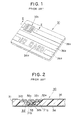
- Fig. 1 shows an external appearance of a conventional IC card
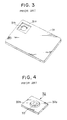
- Fig. 2 is a sectional view taken on a line II-II of Fig. 1 and shows the IC module mounting structure.
- the IC card 30 comprises a plastic card base 31, an IC module 32 embedded in the card base 31, and an overlay 36 on which various ornament patterns and characters 36a are printed.
- the IC module 32 has a plurality of contact patterns 32c which are exposed to the outside.
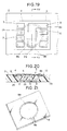
- a first recess 31 a and a second recess 31 b for housing the IC module 32 are formed in the card base 31 as shown in Fig. 3.
- the card base 31 is made by injection molding of ABS resin or by multi-layer laminating PVC (polyvinyl chloride) sheets.
- the IC module 32 is designed in such a way that an IC chip 33 is bonded to a circuit board 32a made of glass epoxy resin, and a seal portion 32b of sealing resin is formed on the circuit board 32a to seal the IC chip 33.
- the contact patterns 32c shown in Fig. 1 are formed on the back side of the circuit board 32a.
- the seal portion 32b of the IC module 32 is housed in the second recess 31 b of the card base 31, and the circuit board 32a is housed in the first recess 31a, while the outer periphery of the circuit board 32a is restricted by the peripheral wall of the first recess 31a, and the surfaces of the contact patterns are coplanar as the card base 31.
- Aliquid adhesive (not shown) is supplied into spaces among the circuit board 32a, the sealing portion 32b, the first recess 31a, and the second recess 31 b, and heated to be solidified.
- the IC module 32 is securely mounted on the card base 31.
- the IC card 30 has a small thickness as about 0.8 mm, and hence it must have an elasticity enough to allow to be bent to a certain extent so as not to be broken by an external force exerted thereon in use. Therefore, it is required that the card base 31 has an elasticity, while the seal portion 32b of the IC module 32 has a rigidity sufficient for protecting the IC module, and that the IC module 32 is firmly fixed to the card base 31.
- the material of the circuit board 32a and the seal portion 32b constituting the IC module 32 is different from that of the card base 31, it is difficult to obtain a liquid adhesive capable of reliably bonding them to each other.
- the adhesive strength in an adhesion state of the IC module changes with the adhered position thereof. Consequently, when the card base 31 is fixed, separation of an adhered portion between the card base 31 and the IC module 32 may occur. As a result, the IC module 32 may separate from the card base 31.
- the liquid adhesive When the liquid adhesive is heated, it can leak from a portion of the gap between the circuit board 32a and the first recess 31 a depending on the amount of the liquid adhesive and the bonding position. As a result, the surface of the overlay 36 on which pattern and characters 36a are printed may be contaminated. In addition, the card base 31 tends to deform because of the heat at the time when the liquid adhesive is heated.
- IC card structure in which the IC module can be secured to the card base without using the liquid adhesive.
- Such IC card structures are shown in Fig. 5 to Fig. 8.
- Fig. 5 to Fig. 8 the same reference numerals as those of Fig. 1 to Fig. 4 designate same parts as Figs. 1 to 4, and hence explanation thereof is omitted hereinafter.
- the IC card structure shown in Fig. 5 is disclosed in U.S. Patent 4,792,843.
- an adhesive sheet 34 (called hot melting sheet) is fitted in the first recess 31 a and the second recess 31 b.
- the IC module 32 is put in the card base 31 so that the seal portion 32b of the IC module 32 and the circuit board 32a are located in the second recess 31 b and the first recess 31 a of the card base 31.
- the upper side of the IC module 32 is heated and downwardly pressed by a heat and pressure applying apparatus (not shown), so that the adhesive sheet 34 laid between the IC module 32 and the first and second recesses 31a and 31 b melts, and solidifies when it cools, thereby fixing the IC module 32 to the card base 31.
- the adhesive sheet is greatly improved in adhesive strength, and hence it is available for assembling IC module.
- the adhesive sheet 34 does not leak from the gap between the IC module 32 and the first and second recesses 31 a and 31b when heat and pressure are applied thereto.
- seal portion 32b sealing the IC chip 33 is required to be formed as thin as possible, a transfer molding method using a thermosetting resin is used for forming the seal portion.
- thermosetting resin is used for forming the seal portion.
- the recesses 31 a and 31 b of the card base 31 are formed when the card base 31 is formed by the injection molding process ofABS resin, or the recesses are formed by cutting the card base after the multi-layer laminating of PVC sheets.
- the ABS resin shrinks when it cools and solidifies, and thus the thickness of the bottom of the second recess 31 decreases and variations have been easily produced in the depth of the second recess 31 b.
- the recess can not be formed with accuracy, causing thickness variance of the bottom of the recess.
- the seal portion 32b of the IC module 32 may project from the second recess 31 b. If the swelled IC module is forcibly packed in the second recess 31 b, the underside of the card base 31 (the opposite surface to the second surface 31 b) swells, thus, deteriorating the external appearance of the IC card.
- U.S. Patent 4,552,383 discloses an IC card which may solve the above described problems.
- Fig. 7 and Fig. 8 show the IC card.
- a reference numeral 40 designates a card base which is provided with a first recess 40a and a second recess 40b.
- An IC module 42 comprises a circuit board 43 having contact patterns 43a on the upper surface thereof, an IC chip 44 mounted on the circuit board 43, and a sealing portion 45 for sealing the IC chip.
- the IC chip 44 and contact patterns 43a are connected to each other by bonding wires and through hole patterns 43b.
- An adhesive sheet 46 is provided only between a peripheral portion of the circuit board 43 and a bottom of the first recess 40a.
- a heat and pressure applying apparatus 41 is set on the upper surface of the circuit board 43 of the IC module 42 to heat and press the IC module.
- the adhesive sheet 46 is melted so that only the peripheral portion of the circuit board 43 is fixed to the bottom of the first recess 40a.
- the peripheral sides of the circuit board 43 engage with the inner wall of the first recess 40a, thereby positioning the IC module 42.
- the second recess 40b has sufficient depth and a capacity to allow shape variation of the seal portion 45 of the IC module 42.
- the IC module 42 is mounted in the first and second recesses 40a and 40b with a space 49 between the seal portion 45 and the bottom of the second recess 40b. However, according to circumstances, the underside of the seal portion 45 may contact with the bottom of the second recess 40b.
- the seal portion 45 has not high accuracy in dimension, it is kept free from the second recess 40b by providing the gap therebetween. Furthermore, only the periphery portion of the circuit board 43 which has high accuracy is fixed to the first recess 40a through the adhesive sheet 46. Consequently, the swelling of the IC module is prevented.
- the IC module is firmly fixed to the card base, but it is also important that the surface of the card base 31 is kept smooth and flat until the overlay or the printing and a hard coat are performed thereon.
- the IC card structure has a defect that a depression is formed in the thin portion 40c of the card base 40 as shown in Fig. 8. This is caused for the following reason.
- the IC module 42 is mounted on the card base 40 with only the periphery portion of the circuit board 43, fixed on the first recess 40a through the adhesive sheet 46.
- the heat and pressure applying apparatus 41 set on the circuit board 43 heats the adhesive sheet 46, the heat is transmitted not only to the adhesive sheet 46 but also to the card base 40, thereby heating the air in the space 49 between the seal portion 45 and the second recess 40b. While being heated, the air in the space 49 is expanded. Therefore, the thin portion 40c projects outwardly and a apart of the air discharges from the space 49.
- the temperature of the air in the space 49 falls to a normal temperature, so that the volume of the air decreases and the pressure in the space is decompressed.
- the pressure of the air in the space becomes lower than the atmospheric pressure, so that the thin portion 40c is pushed into the space to produce a depression 47 as shown in Figure 8.
- the depression 47 causes incomplete adhesion between the hard coat and the card base, and hence the printing on the hard coat may be bad at the depression.
- the object of the present invention is to provide an IC card in which the IC module is fixed to the card base by a thermo reactive adhesive without forming a depression on the card base.
- an IC card comprising:
- the opening is formed in the card base.
- the opening is a through hole formed in the circuit board for connecting the contact pattern with the IC chip.
- an IC card 1 comprises a card base 2 having a first recess 2a, a second recess 2b, an IC module 3, and an adhesive sheet 8.
- the second recess 2b has a circular shape in plan view and is positioned at a central portion of the first recess 2a as shown in Fig. 9.
- Athin portion 2c defining the bottom of the second recess 2b has an opening 2d.
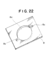
- the adhesive sheet 8 has an opening 8a for receiving the IC module 3.
- the IC module 3 comprises a circuit board 4 having a contact patterns 5 formed on the upper surface thereof, an IC chip 6 mounted on the underside of the circuit board 4, and a seal portion 7 which seals the IC chip 6 by the transfer molding method using a thermosetting resin.
- the IC chip 6 and contact patterns 5 are connected by bonding wires and through hole electrodes 5a.
- the adhesive sheet 8 is put in the first recess 2a and the circuit board 4 of the IC module is put on the adhesive sheet.
- the outer peripheral sides of the circuit board 4 are restricted by inner walls of the first recess 2a, and only the underside of the peripheral portion of the circuit board 2a is fixed to the first recess 2a through the adhesive sheet 8.
- the seal portion 7 of the IC module 3 is housed in the second recess 2b.
- the air in the space 9 expands with the heating of the IC module 3, a part of the air discharges from the space 9 passing through the opening 2d, and hence the pressure difference between the space 9 and the atmosphere does not occur.
- the thin portion 2c is not depressed when cooled, because the space 9 is not decompressed through the opening 2d.
- the opening 2d is filled with a seal member 11 such as an adhesive as shown in Fig. 10.
- an overlay or a hard coat is adhered on the card base 2 to cover the seal member 11.
- seal member 11 may be omitted as shown in Fig. 12, because the opening 2d of the card base 2 is perfectly closed by an overlay 12.
- the circuit board 4 has an opening 4a at such a position that the space 9 and the atmosphere are communicated with each other through the opening 4a.
- the opening is formed at the time when through hole electrodes 5a are formed in the contact patterns 5.
- an indentation 2e is formed in the inner wall of the second recess 2b to widen the space, and the opening 4a is formed to communicate with the widened space as shown in Fig. 14.
- the IC card is characterized in that the space 9 in the second recess 2b communicates with the atmosphere through the through hole electrodes 5a. More particularly, a pair of through hole electrodes 5a which are positioned symmetrically about the center of the second recess 2b are selected, each of which communicates with the space 9 through a groove 2f formed in the bottom of the first recess 2a. A pair of slits 8c are further provided in the adhesive sheet 8 so as to communicate the groove 2f with the through hole electrode 5a.
- Figs. 17 and 18 show the fourth embodiment of the present invention.
- An opening 10 is formed in the card base 2, and the groove 2f is formed in the first recess 2a so as to communicate the space 9 with the opening 10.
- the adhesive sheet 8 a notch is previously formed for communicating the opening 10 with groove 2f.
- the overlay orthe printing and the hard coat are not shown in the drawings, it is applied to the card base 2 so as to hide the opening 10.
- the adhesive sheet 8 has a slit 8b communicating with the opening 8a for the IC module 3, and an opening 10 constituted by a notch 2g is formed in the card base 2 so as to be communicated with the slit 8b.
- the space 9 communicates with the atmosphere through the slit 8b and the opening 10.
- the IC module is mounted in the card base in such a way that the seal portion of the IC module is positioned in the second recess of the card base with a space between the card base and IC module, and the circuit board of the 10 module is fixed to the first recess of the card base with the thermo reactive adhesive sheet, and the IC card is provided with an opening for discharging the air from the space.
- the opening can be formed at a desired position in the card base and the circuit board of the IC module.
Landscapes
- Engineering & Computer Science (AREA)
- Computer Hardware Design (AREA)
- Microelectronics & Electronic Packaging (AREA)
- Physics & Mathematics (AREA)
- General Physics & Mathematics (AREA)
- Theoretical Computer Science (AREA)
- Credit Cards Or The Like (AREA)
Abstract
Description
- The present invention relates to an IC (integrated circuit) card, and more particularly to structure for securing an IC module to a card base.
- The IC card has an IC chip having a CPU and memories. Since the recent IC card has a larger storage capacity than a conventional IC card, its use in place of a bankbook or a credit card is into consideration.
- The IC module including the IC chip is mounted in the IC card. However, there are various problems in the mounting of the IC module.
- Japanese Patent Application Laid-open 63-94646 and Japanese Utility Model Application Laid-open 61-46655 disclose IC module mounting structure.
- Fig. 1 shows an external appearance of a conventional IC card and Fig. 2 is a sectional view taken on a line II-II of Fig. 1 and shows the IC module mounting structure.
- The
IC card 30 comprises aplastic card base 31, anIC module 32 embedded in thecard base 31, and anoverlay 36 on which various ornament patterns andcharacters 36a are printed. TheIC module 32 has a plurality ofcontact patterns 32c which are exposed to the outside. - Describing the mounting of the IC module, a
first recess 31 a and asecond recess 31 b for housing theIC module 32 are formed in thecard base 31 as shown in Fig. 3. Thecard base 31 is made by injection molding of ABS resin or by multi-layer laminating PVC (polyvinyl chloride) sheets. As shown in Fig. 4, theIC module 32 is designed in such a way that anIC chip 33 is bonded to acircuit board 32a made of glass epoxy resin, and aseal portion 32b of sealing resin is formed on thecircuit board 32a to seal theIC chip 33. On the other hand, thecontact patterns 32c shown in Fig. 1 are formed on the back side of thecircuit board 32a. - As shown in Fig. 2, the
seal portion 32b of theIC module 32 is housed in thesecond recess 31 b of thecard base 31, and thecircuit board 32a is housed in thefirst recess 31a, while the outer periphery of thecircuit board 32a is restricted by the peripheral wall of thefirst recess 31a, and the surfaces of the contact patterns are coplanar as thecard base 31. Aliquid adhesive (not shown) is supplied into spaces among thecircuit board 32a, thesealing portion 32b, thefirst recess 31a, and thesecond recess 31 b, and heated to be solidified. Thus, theIC module 32 is securely mounted on thecard base 31. - Generally, the
IC card 30 has a small thickness as about 0.8 mm, and hence it must have an elasticity enough to allow to be bent to a certain extent so as not to be broken by an external force exerted thereon in use. Therefore, it is required that thecard base 31 has an elasticity, while theseal portion 32b of theIC module 32 has a rigidity sufficient for protecting the IC module, and that theIC module 32 is firmly fixed to thecard base 31. - Since the material of the
circuit board 32a and theseal portion 32b constituting theIC module 32 is different from that of thecard base 31, it is difficult to obtain a liquid adhesive capable of reliably bonding them to each other. In addition, the adhesive strength in an adhesion state of the IC module changes with the adhered position thereof. Consequently, when thecard base 31 is fixed, separation of an adhered portion between thecard base 31 and theIC module 32 may occur. As a result, theIC module 32 may separate from thecard base 31. - When the liquid adhesive is heated, it can leak from a portion of the gap between the
circuit board 32a and the first recess 31 a depending on the amount of the liquid adhesive and the bonding position. As a result, the surface of theoverlay 36 on which pattern andcharacters 36a are printed may be contaminated. In addition, thecard base 31 tends to deform because of the heat at the time when the liquid adhesive is heated. - Moreover, the liquid adhesive inherently has poor handling properties and workability. Therefore, there has been a demand for IC card structure in which the IC module can be secured to the card base without using the liquid adhesive. Such IC card structures are shown in Fig. 5 to Fig. 8. In Fig. 5 to Fig. 8, the same reference numerals as those of Fig. 1 to Fig. 4 designate same parts as Figs. 1 to 4, and hence explanation thereof is omitted hereinafter.
- The IC card structure shown in Fig. 5 is disclosed in U.S. Patent 4,792,843. In assembling the
IC module 32, an adhesive sheet 34 (called hot melting sheet) is fitted in thefirst recess 31 a and thesecond recess 31 b. TheIC module 32 is put in thecard base 31 so that theseal portion 32b of theIC module 32 and thecircuit board 32a are located in thesecond recess 31 b and thefirst recess 31 a of thecard base 31. The upper side of theIC module 32 is heated and downwardly pressed by a heat and pressure applying apparatus (not shown), so that theadhesive sheet 34 laid between theIC module 32 and the first andsecond recesses IC module 32 to thecard base 31. - Recently, the adhesive sheet is greatly improved in adhesive strength, and hence it is available for assembling IC module. In particular, the
adhesive sheet 34 does not leak from the gap between theIC module 32 and the first andsecond recesses - However, there is a problem that the upper surface of the
circuit board 32a swells as shown in Fig. 6. It is thought that the swelling occurs from the following reason. - Since the
seal portion 32b sealing theIC chip 33 is required to be formed as thin as possible, a transfer molding method using a thermosetting resin is used for forming the seal portion. However, there are considerable variations in dimension of the solidified seal portions formed by the transfer molding method. - On the other hand, the
recesses card base 31 are formed when thecard base 31 is formed by the injection molding process ofABS resin, or the recesses are formed by cutting the card base after the multi-layer laminating of PVC sheets. - In the injection molding process, the ABS resin shrinks when it cools and solidifies, and thus the thickness of the bottom of the
second recess 31 decreases and variations have been easily produced in the depth of thesecond recess 31 b. In the cutting process, the recess can not be formed with accuracy, causing thickness variance of the bottom of the recess. - If the IC module is formed thick and the
card base 31 is formed into a shallow second recess, theseal portion 32b of theIC module 32 may project from thesecond recess 31 b. If the swelled IC module is forcibly packed in thesecond recess 31 b, the underside of the card base 31 (the opposite surface to thesecond surface 31 b) swells, thus, deteriorating the external appearance of the IC card. - U.S. Patent 4,552,383 discloses an IC card which may solve the above described problems. Fig. 7 and Fig. 8 show the IC card. In Fig. 7, a
reference numeral 40 designates a card base which is provided with afirst recess 40a and asecond recess 40b. An IC module 42 comprises acircuit board 43 havingcontact patterns 43a on the upper surface thereof, anIC chip 44 mounted on thecircuit board 43, and asealing portion 45 for sealing the IC chip. TheIC chip 44 andcontact patterns 43a are connected to each other by bonding wires and through hole patterns 43b. Anadhesive sheet 46 is provided only between a peripheral portion of thecircuit board 43 and a bottom of thefirst recess 40a. A heat andpressure applying apparatus 41 is set on the upper surface of thecircuit board 43 of the IC module 42 to heat and press the IC module. Thus, theadhesive sheet 46 is melted so that only the peripheral portion of thecircuit board 43 is fixed to the bottom of thefirst recess 40a. - The peripheral sides of the
circuit board 43 engage with the inner wall of thefirst recess 40a, thereby positioning the IC module 42. Thesecond recess 40b has sufficient depth and a capacity to allow shape variation of theseal portion 45 of the IC module 42. The IC module 42 is mounted in the first andsecond recesses space 49 between theseal portion 45 and the bottom of thesecond recess 40b. However, according to circumstances, the underside of theseal portion 45 may contact with the bottom of thesecond recess 40b. - Although the
seal portion 45 has not high accuracy in dimension, it is kept free from thesecond recess 40b by providing the gap therebetween. Furthermore, only the periphery portion of thecircuit board 43 which has high accuracy is fixed to thefirst recess 40a through theadhesive sheet 46. Consequently, the swelling of the IC module is prevented. - As mentioned above, it is most important in the IC card that the IC module is firmly fixed to the card base, but it is also important that the surface of the
card base 31 is kept smooth and flat until the overlay or the printing and a hard coat are performed thereon. - However, the IC card structure has a defect that a depression is formed in the
thin portion 40c of thecard base 40 as shown in Fig. 8. This is caused for the following reason. As shown in Fig. 7, the IC module 42 is mounted on thecard base 40 with only the periphery portion of thecircuit board 43, fixed on thefirst recess 40a through theadhesive sheet 46. When the heat andpressure applying apparatus 41 set on thecircuit board 43 heats theadhesive sheet 46, the heat is transmitted not only to theadhesive sheet 46 but also to thecard base 40, thereby heating the air in thespace 49 between theseal portion 45 and thesecond recess 40b. While being heated, the air in thespace 49 is expanded. Therefore, thethin portion 40c projects outwardly and a apart of the air discharges from thespace 49. When the card base is cooled, the temperature of the air in thespace 49 falls to a normal temperature, so that the volume of the air decreases and the pressure in the space is decompressed. Thus, the pressure of the air in the space becomes lower than the atmospheric pressure, so that thethin portion 40c is pushed into the space to produce adepression 47 as shown in Figure 8. Thedepression 47 causes incomplete adhesion between the hard coat and the card base, and hence the printing on the hard coat may be bad at the depression. - The object of the present invention is to provide an IC card in which the IC module is fixed to the card base by a thermo reactive adhesive without forming a depression on the card base.
- According to this invention there is provided an IC card comprising:
- a card base made of synthetic resin and having a first recess and a second recess formed in said first recess; and
- an IC module having a circuit board, contact patterns formed on said circuit board, an IC chip mounted on said circuit board, and a seal portion sealing said IC chip;
- said IC module being mounted on said card base such that said seal portion of said IC module is positioned in said second recess with a space between the card base and said IC module, and said circuit board of said IC module being fixed on said first recess of said card base by a thermo reactive adhesive sheet,
- characterised in that there is provided an opening between said space and the outer surface of said IC card.
- In an aspect of the invention, the opening is formed in the card base.
- In another aspect, the opening is a through hole formed in the circuit board for connecting the contact pattern with the IC chip.
- The objects and features of the present invention will become more apparent from the following detailed description with reference to the accompanying drawings.
-
- Figure 1 is a perspective view showing a conventional IC card;
- Figure 2 is a sectional view taken along a line II-II of Figure 1;
- Figure 3 is a perspective view showing a card base of the conventional IC card;
- Figure 4 is a perspective view showing an IC module to be mounted in the IC card;
- Figure 5 is an exploded sectional view showing a main part of another conventional IC card;
- Fig. 6 is a sectional view showing the internal structure of the conventional IC card of Fig. 5;
- Fig. 7 is a sectional view of a main part of still another conventional IC card, which shows a step during a manufacturing process;
- Fig. 8 is a sectional view showing the finished IC card after the step of Fig. 7;
- Fig. 9 is a plan view showing a main part of an IC card according to a first embodiment of the present invention;
- Fig. 10 is a sectional view taken along a line X-X of Fig. 9;
- Fig. 11 is a perspective view showing an adhesive sheet used in the present invention;
- Fig. 12 is a sectional view showing a main part of IC card according to an improvement of the first embodiment of the present invention;
- Fig. 13 is a plan view showing a main part of an IC card according to a second embodiment of the present invention;
- Fig. 14 is a sectional view taken along a line XIV-XIV of Fig. 13;
- Fig. 15 is a plan view showing a main part of an IC card according to a third embodiment of the present invention;
- Fig. 16 is a sectional view taken along a line XVI-XVI of Fig. 15;
- Fig. 17 is a plan view showing a main part of an IC card according to a fourth embodiment of the present invention;
- Fig. 18 is a sectional view taken along a line XVIII-XVIII of Fig. 17;
- Fig. 19 is a plan view showing a main part of an IC card according to a fifth embodiment of the present invention;
- Fig. 20 is a sectional view taken along a line XX-XX of Fig. 19;
- Fig. 21 is a perspective view showing another adhesive sheet used in the present invention; and
- Fig. 22 is a perspective view showing still another adhesive sheet used in the present invention.
- The present invention will now be described in detail with reference to the drawings.
- Referring to Figs. 9 and 10, an
IC card 1 comprises acard base 2 having afirst recess 2a, asecond recess 2b, anIC module 3, and anadhesive sheet 8. Thesecond recess 2b has a circular shape in plan view and is positioned at a central portion of thefirst recess 2a as shown in Fig. 9.Athin portion 2c defining the bottom of thesecond recess 2b has anopening 2d. As shown in Fig. 11, theadhesive sheet 8 has anopening 8a for receiving theIC module 3. - The
IC module 3 comprises acircuit board 4 having acontact patterns 5 formed on the upper surface thereof, anIC chip 6 mounted on the underside of thecircuit board 4, and aseal portion 7 which seals theIC chip 6 by the transfer molding method using a thermosetting resin. TheIC chip 6 andcontact patterns 5 are connected by bonding wires and throughhole electrodes 5a. Theadhesive sheet 8 is put in thefirst recess 2a and thecircuit board 4 of the IC module is put on the adhesive sheet. The outer peripheral sides of thecircuit board 4 are restricted by inner walls of thefirst recess 2a, and only the underside of the peripheral portion of thecircuit board 2a is fixed to thefirst recess 2a through theadhesive sheet 8. Theseal portion 7 of theIC module 3 is housed in thesecond recess 2b. - When the air in the
space 9 expands with the heating of theIC module 3, a part of the air discharges from thespace 9 passing through theopening 2d, and hence the pressure difference between thespace 9 and the atmosphere does not occur. On the other hand, after applying heat and pressure, thethin portion 2c is not depressed when cooled, because thespace 9 is not decompressed through theopening 2d. Theopening 2d is filled with aseal member 11 such as an adhesive as shown in Fig. 10. Moreover, an overlay or a hard coat is adhered on thecard base 2 to cover theseal member 11. - However, the
seal member 11 may be omitted as shown in Fig. 12, because theopening 2d of thecard base 2 is perfectly closed by anoverlay 12. - Referring to Figs. 13 and 14 showing the second embodiment of the present invention, the
circuit board 4 has anopening 4a at such a position that thespace 9 and the atmosphere are communicated with each other through theopening 4a. The opening is formed at the time when throughhole electrodes 5a are formed in thecontact patterns 5. - However, it may be difficult to form the
opening 4a at a desired position so as to communicate with the space between the peripheral side wall and the inner wall of thesecond recess 2b, because the width of the space is small. In order to solve such a problem, anindentation 2e is formed in the inner wall of thesecond recess 2b to widen the space, and theopening 4a is formed to communicate with the widened space as shown in Fig. 14. - Referring to Figs. 15,16 and 22 showing the third embodiment, the IC card is characterized in that the
space 9 in thesecond recess 2b communicates with the atmosphere through the throughhole electrodes 5a. More particularly, a pair of throughhole electrodes 5a which are positioned symmetrically about the center of thesecond recess 2b are selected, each of which communicates with thespace 9 through agroove 2f formed in the bottom of thefirst recess 2a. A pair ofslits 8c are further provided in theadhesive sheet 8 so as to communicate thegroove 2f with the throughhole electrode 5a. - In the third embodiment, since the through
hole electrodes 5a are used for the opening for thespace 9, additional openings are not provided in the surface of the IC card. Thus, an IC card without defects can be produced. - Figs. 17 and 18 show the fourth embodiment of the present invention. An
opening 10 is formed in thecard base 2, and thegroove 2f is formed in thefirst recess 2a so as to communicate thespace 9 with theopening 10. In theadhesive sheet 8, a notch is previously formed for communicating theopening 10 withgroove 2f. Although the overlay orthe printing and the hard coat are not shown in the drawings, it is applied to thecard base 2 so as to hide theopening 10. - Referring to Figs. 19 to 21 showing the fifth embodiment, the
adhesive sheet 8 has aslit 8b communicating with theopening 8a for theIC module 3, and anopening 10 constituted by a notch 2g is formed in thecard base 2 so as to be communicated with theslit 8b. Thus, thespace 9 communicates with the atmosphere through theslit 8b and theopening 10. - As is apparent from the above description, in the IC card structure of the present invention, the IC module is mounted in the card base in such a way that the seal portion of the IC module is positioned in the second recess of the card base with a space between the card base and IC module, and the circuit board of the 10 module is fixed to the first recess of the card base with the thermo reactive adhesive sheet, and the IC card is provided with an opening for discharging the air from the space. Thus, some of the air in the space is discharged through the opening when the air expands. Consequently, the card base does not deform. In addition, the opening can be formed at a desired position in the card base and the circuit board of the IC module.
- While the invention has been described in conjunction with preferred specific embodiments thereof, it will be understood that this description is intended to illustrate and not limit the scope of the invention, which is defined by the following claims.
Claims (13)
Applications Claiming Priority (2)
| Application Number | Priority Date | Filing Date | Title |
|---|---|---|---|
| JP28190789 | 1989-10-31 | ||
| JP281907/89 | 1989-10-31 |
Publications (4)
| Publication Number | Publication Date |
|---|---|
| EP0426406A2 EP0426406A2 (en) | 1991-05-08 |
| EP0426406A3 EP0426406A3 (en) | 1993-03-24 |
| EP0426406B1 true EP0426406B1 (en) | 1995-05-10 |
| EP0426406B2 EP0426406B2 (en) | 1998-08-19 |
Family
ID=17645621
Family Applications (1)
| Application Number | Title | Priority Date | Filing Date |
|---|---|---|---|
| EP90311820A Expired - Lifetime EP0426406B2 (en) | 1989-10-31 | 1990-10-29 | IC card having an integrated circuit module |
Country Status (6)
| Country | Link |
|---|---|
| EP (1) | EP0426406B2 (en) |
| JP (1) | JP3095766B2 (en) |
| AT (1) | ATE122485T1 (en) |
| CA (1) | CA2027823C (en) |
| DE (1) | DE69019298T3 (en) |
| ES (1) | ES2074139T5 (en) |
Families Citing this family (19)
| Publication number | Priority date | Publication date | Assignee | Title |
|---|---|---|---|---|
| JPH07182471A (en) * | 1991-01-10 | 1995-07-21 | Nec Corp | Ic card |
| FR2684471B1 (en) * | 1991-12-02 | 1994-03-04 | Solaic | METHOD FOR MANUFACTURING A MEMORY CARD AND MEMORY CARD THUS OBTAINED. |
| DE4209184C1 (en) * | 1992-03-21 | 1993-05-19 | Orga Kartensysteme Gmbh, 6072 Dreieich, De | |
| JPH06166286A (en) * | 1992-11-30 | 1994-06-14 | Sony Corp | Thermocompression bonding method for memory card and contact bonder |
| US5956601A (en) * | 1996-04-25 | 1999-09-21 | Kabushiki Kaisha Toshiba | Method of mounting a plurality of semiconductor devices in corresponding supporters |
| DE29709618U1 (en) * | 1997-06-03 | 1997-08-07 | Sternberg, Dirk, 94568 St Oswald | Chip card and card adapter |
| FR2794552B1 (en) * | 1999-06-03 | 2001-08-31 | Gemplus Card Int | METHOD FOR HOT BONDING OF AN ELECTRONIC MODULE IN A CHIP CARD |
| GB2352999A (en) * | 1999-07-21 | 2001-02-14 | Allan Walter Sills | Smart card with chip carrier with contact pads fitted into aperture of card base |
| EP2418608A1 (en) * | 2010-07-23 | 2012-02-15 | Gemalto SA | Secure electronic module, device with secure electronic module and manufacturing method |
| EP3168788A1 (en) | 2015-11-11 | 2017-05-17 | Mastercard International Incorporated | Integrated circuit card |
| EP3168787A1 (en) | 2015-11-11 | 2017-05-17 | Mastercard International Incorporated | Integrated circuit card |
| US11618191B2 (en) | 2016-07-27 | 2023-04-04 | Composecure, Llc | DI metal transaction devices and processes for the manufacture thereof |
| CN109564634B (en) | 2016-07-27 | 2026-04-14 | 安全创造有限责任公司 | Overmolded electronic component for transaction cards and method of making same |
| US10762412B2 (en) | 2018-01-30 | 2020-09-01 | Composecure, Llc | DI capacitive embedded metal card |
| US10977540B2 (en) | 2016-07-27 | 2021-04-13 | Composecure, Llc | RFID device |
| US11151437B2 (en) | 2017-09-07 | 2021-10-19 | Composecure, Llc | Metal, ceramic, or ceramic-coated transaction card with window or window pattern and optional backlighting |
| NZ762589A (en) | 2017-09-07 | 2022-05-27 | Composecure Llc | Transaction card with embedded electronic components and process for manufacture |
| KR102931665B1 (en) | 2017-10-18 | 2026-02-26 | 컴포시큐어 엘.엘.씨. | Metal, ceramic, or ceramic-coated transaction card with window or window pattern and optional backlighting |
| JP7485005B1 (en) * | 2022-12-19 | 2024-05-16 | 株式会社レゾナック | Method for manufacturing joined body, joined body, and electric/electronic component |
Family Cites Families (2)
| Publication number | Priority date | Publication date | Assignee | Title |
|---|---|---|---|---|
| DE3151408C1 (en) * | 1981-12-24 | 1983-06-01 | GAO Gesellschaft für Automation und Organisation mbH, 8000 München | ID card with an IC module |
| DE3338597A1 (en) * | 1983-10-24 | 1985-05-02 | GAO Gesellschaft für Automation und Organisation mbH, 8000 München | DATA CARRIER WITH INTEGRATED CIRCUIT AND METHOD FOR PRODUCING THE SAME |
-
1990
- 1990-10-17 CA CA002027823A patent/CA2027823C/en not_active Expired - Fee Related
- 1990-10-23 JP JP02283422A patent/JP3095766B2/en not_active Expired - Fee Related
- 1990-10-29 DE DE69019298T patent/DE69019298T3/en not_active Expired - Fee Related
- 1990-10-29 ES ES90311820T patent/ES2074139T5/en not_active Expired - Lifetime
- 1990-10-29 AT AT90311820T patent/ATE122485T1/en active
- 1990-10-29 EP EP90311820A patent/EP0426406B2/en not_active Expired - Lifetime
Also Published As
| Publication number | Publication date |
|---|---|
| DE69019298T3 (en) | 1999-04-15 |
| CA2027823C (en) | 1994-11-08 |
| EP0426406B2 (en) | 1998-08-19 |
| EP0426406A2 (en) | 1991-05-08 |
| CA2027823A1 (en) | 1991-05-01 |
| DE69019298D1 (en) | 1995-06-14 |
| JPH03205197A (en) | 1991-09-06 |
| ES2074139T5 (en) | 1999-01-01 |
| JP3095766B2 (en) | 2000-10-10 |
| DE69019298T2 (en) | 1996-01-04 |
| EP0426406A3 (en) | 1993-03-24 |
| ES2074139T3 (en) | 1995-09-01 |
| ATE122485T1 (en) | 1995-05-15 |
Similar Documents
| Publication | Publication Date | Title |
|---|---|---|
| EP0426406B2 (en) | IC card having an integrated circuit module | |
| US4994659A (en) | IC card | |
| US5026452A (en) | Method of producing IC cards | |
| US5346576A (en) | Method of manufacturing IC card | |
| US5272374A (en) | Production method for an IC card and its IC card | |
| JPH0130149B2 (en) | ||
| JP2849594B2 (en) | Electronic module sealing method | |
| US4417413A (en) | Identification card with IC chip and a method for manufacturing the same | |
| JP2812485B2 (en) | Manufacturing method of memory card | |
| US4463971A (en) | Identification card having an IC module | |
| AU726884B2 (en) | Method of making smart cards | |
| US4904429A (en) | Method of producing a molding of foamed resin having a section for fitting an electrical part | |
| US5935497A (en) | Method of printing a graphic on a memory card | |
| US5514240A (en) | Method for incorporating a carrier element | |
| US7320738B2 (en) | Method for encapsulation of a chip card and module obtained thus | |
| WO2002028613A1 (en) | Moulding apparatus and method | |
| JP2001084347A (en) | Card type storage device and method of manufacturing the same | |
| JPH0417343A (en) | Manufacture of thin-type semiconductor device | |
| JPH02301155A (en) | Method of fixing ic module | |
| US5877544A (en) | Electronic micropackage for an electronic memory card | |
| JPH03114788A (en) | Structure of ic card | |
| KR0129760B1 (en) | Substrate with a protective film and optical memory device manufacturing method using the same | |
| JPH09183284A (en) | Non-contact-type ic card and manufacture thereof | |
| JP3126782B2 (en) | Method for manufacturing thin semiconductor device | |
| JPH0262398B2 (en) |
Legal Events
| Date | Code | Title | Description |
|---|---|---|---|
| PUAI | Public reference made under article 153(3) epc to a published international application that has entered the european phase |
Free format text: ORIGINAL CODE: 0009012 |
|
| AK | Designated contracting states |
Kind code of ref document: A2 Designated state(s): AT BE CH DE ES FR GB IT LI LU NL SE |
|
| PUAL | Search report despatched |
Free format text: ORIGINAL CODE: 0009013 |
|
| AK | Designated contracting states |
Kind code of ref document: A3 Designated state(s): AT BE CH DE ES FR GB IT LI LU NL SE |
|
| 17P | Request for examination filed |
Effective date: 19930621 |
|
| 17Q | First examination report despatched |
Effective date: 19931119 |
|
| GRAA | (expected) grant |
Free format text: ORIGINAL CODE: 0009210 |
|
| AK | Designated contracting states |
Kind code of ref document: B1 Designated state(s): AT BE CH DE ES FR GB IT LI LU NL SE |
|
| REF | Corresponds to: |
Ref document number: 122485 Country of ref document: AT Date of ref document: 19950515 Kind code of ref document: T |
|
| REF | Corresponds to: |
Ref document number: 69019298 Country of ref document: DE Date of ref document: 19950614 |
|
| ITF | It: translation for a ep patent filed | ||
| ET | Fr: translation filed | ||
| REG | Reference to a national code |
Ref country code: ES Ref legal event code: FG2A Ref document number: 2074139 Country of ref document: ES Kind code of ref document: T3 |
|
| PLBI | Opposition filed |
Free format text: ORIGINAL CODE: 0009260 |
|
| PLAB | Opposition data, opponent's data or that of the opponent's representative modified |
Free format text: ORIGINAL CODE: 0009299OPPO |
|
| PLBQ | Unpublished change to opponent data |
Free format text: ORIGINAL CODE: EPIDOS OPPO |
|
| PLBF | Reply of patent proprietor to notice(s) of opposition |
Free format text: ORIGINAL CODE: EPIDOS OBSO |
|
| 26 | Opposition filed |
Opponent name: GIESECKE & DEVRIENT GMBH Effective date: 19960209 |
|
| R26 | Opposition filed (corrected) |
Opponent name: GIESECKE & DEVRIENT GMBH Effective date: 19960209 |
|
| NLR1 | Nl: opposition has been filed with the epo |
Opponent name: GIESECKE & DEVRIENT GMBH |
|
| PLBF | Reply of patent proprietor to notice(s) of opposition |
Free format text: ORIGINAL CODE: EPIDOS OBSO |
|
| PLAW | Interlocutory decision in opposition |
Free format text: ORIGINAL CODE: EPIDOS IDOP |
|
| PLAW | Interlocutory decision in opposition |
Free format text: ORIGINAL CODE: EPIDOS IDOP |
|
| ITF | It: translation for a ep patent filed | ||
| PLAW | Interlocutory decision in opposition |
Free format text: ORIGINAL CODE: EPIDOS IDOP |
|
| PUAH | Patent maintained in amended form |
Free format text: ORIGINAL CODE: 0009272 |
|
| STAA | Information on the status of an ep patent application or granted ep patent |
Free format text: STATUS: PATENT MAINTAINED AS AMENDED |
|
| 27A | Patent maintained in amended form |
Effective date: 19980819 |
|
| AK | Designated contracting states |
Kind code of ref document: B2 Designated state(s): AT BE CH DE ES FR GB IT LI LU NL SE |
|
| REG | Reference to a national code |
Ref country code: CH Ref legal event code: AEN Free format text: MAINTIEN DU BREVET DONT L'ETENDUE A ETE MODIFIEE |
|
| NLR2 | Nl: decision of opposition | ||
| NLR3 | Nl: receipt of modified translations in the netherlands language after an opposition procedure | ||
| PGFP | Annual fee paid to national office [announced via postgrant information from national office to epo] |
Ref country code: ES Payment date: 19981019 Year of fee payment: 9 |
|
| ET3 | Fr: translation filed ** decision concerning opposition | ||
| REG | Reference to a national code |
Ref country code: ES Ref legal event code: DC2A Kind code of ref document: T5 Effective date: 19981118 |
|
| PGFP | Annual fee paid to national office [announced via postgrant information from national office to epo] |
Ref country code: SE Payment date: 19991007 Year of fee payment: 10 |
|
| PGFP | Annual fee paid to national office [announced via postgrant information from national office to epo] |
Ref country code: FR Payment date: 19991011 Year of fee payment: 10 |
|
| PGFP | Annual fee paid to national office [announced via postgrant information from national office to epo] |
Ref country code: AT Payment date: 19991013 Year of fee payment: 10 |
|
| PGFP | Annual fee paid to national office [announced via postgrant information from national office to epo] |
Ref country code: LU Payment date: 19991022 Year of fee payment: 10 |
|
| PGFP | Annual fee paid to national office [announced via postgrant information from national office to epo] |
Ref country code: GB Payment date: 19991027 Year of fee payment: 10 Ref country code: CH Payment date: 19991027 Year of fee payment: 10 |
|
| PGFP | Annual fee paid to national office [announced via postgrant information from national office to epo] |
Ref country code: NL Payment date: 19991029 Year of fee payment: 10 |
|
| PGFP | Annual fee paid to national office [announced via postgrant information from national office to epo] |
Ref country code: DE Payment date: 19991102 Year of fee payment: 10 |
|
| PGFP | Annual fee paid to national office [announced via postgrant information from national office to epo] |
Ref country code: BE Payment date: 19991221 Year of fee payment: 10 |
|
| PG25 | Lapsed in a contracting state [announced via postgrant information from national office to epo] |
Ref country code: LU Free format text: LAPSE BECAUSE OF NON-PAYMENT OF DUE FEES Effective date: 20001029 Ref country code: GB Free format text: LAPSE BECAUSE OF NON-PAYMENT OF DUE FEES Effective date: 20001029 Ref country code: AT Free format text: LAPSE BECAUSE OF NON-PAYMENT OF DUE FEES Effective date: 20001029 |
|
| PG25 | Lapsed in a contracting state [announced via postgrant information from national office to epo] |
Ref country code: SE Free format text: THE PATENT HAS BEEN ANNULLED BY A DECISION OF A NATIONAL AUTHORITY Effective date: 20001030 Ref country code: ES Free format text: LAPSE BECAUSE OF NON-PAYMENT OF DUE FEES Effective date: 20001030 |
|
| PG25 | Lapsed in a contracting state [announced via postgrant information from national office to epo] |
Ref country code: LI Free format text: LAPSE BECAUSE OF NON-PAYMENT OF DUE FEES Effective date: 20001031 Ref country code: CH Free format text: LAPSE BECAUSE OF NON-PAYMENT OF DUE FEES Effective date: 20001031 Ref country code: BE Free format text: LAPSE BECAUSE OF NON-PAYMENT OF DUE FEES Effective date: 20001031 |
|
| BERE | Be: lapsed |
Owner name: CITIZEN WATCH CO. LTD Effective date: 20001031 |
|
| PG25 | Lapsed in a contracting state [announced via postgrant information from national office to epo] |
Ref country code: NL Free format text: LAPSE BECAUSE OF NON-PAYMENT OF DUE FEES Effective date: 20010501 |
|
| REG | Reference to a national code |
Ref country code: CH Ref legal event code: PL |
|
| EUG | Se: european patent has lapsed |
Ref document number: 90311820.6 |
|
| GBPC | Gb: european patent ceased through non-payment of renewal fee |
Effective date: 20001029 |
|
| PG25 | Lapsed in a contracting state [announced via postgrant information from national office to epo] |
Ref country code: FR Free format text: LAPSE BECAUSE OF NON-PAYMENT OF DUE FEES Effective date: 20010629 |
|
| NLV4 | Nl: lapsed or anulled due to non-payment of the annual fee |
Effective date: 20010501 |
|
| PG25 | Lapsed in a contracting state [announced via postgrant information from national office to epo] |
Ref country code: DE Free format text: LAPSE BECAUSE OF NON-PAYMENT OF DUE FEES Effective date: 20010703 |
|
| REG | Reference to a national code |
Ref country code: FR Ref legal event code: ST |
|
| REG | Reference to a national code |
Ref country code: ES Ref legal event code: FD2A Effective date: 20011113 |
|
| PG25 | Lapsed in a contracting state [announced via postgrant information from national office to epo] |
Ref country code: IT Free format text: LAPSE BECAUSE OF NON-PAYMENT OF DUE FEES;WARNING: LAPSES OF ITALIAN PATENTS WITH EFFECTIVE DATE BEFORE 2007 MAY HAVE OCCURRED AT ANY TIME BEFORE 2007. THE CORRECT EFFECTIVE DATE MAY BE DIFFERENT FROM THE ONE RECORDED. Effective date: 20051029 |