EP0425971A2 - Vollisolierter Kondensator und Verfahren zu seiner Herstellung - Google Patents
Vollisolierter Kondensator und Verfahren zu seiner Herstellung Download PDFInfo
- Publication number
- EP0425971A2 EP0425971A2 EP90120257A EP90120257A EP0425971A2 EP 0425971 A2 EP0425971 A2 EP 0425971A2 EP 90120257 A EP90120257 A EP 90120257A EP 90120257 A EP90120257 A EP 90120257A EP 0425971 A2 EP0425971 A2 EP 0425971A2
- Authority
- EP
- European Patent Office
- Prior art keywords
- oxide
- mole percent
- additive
- silicon dioxide
- degrees
- Prior art date
- Legal status (The legal status is an assumption and is not a legal conclusion. Google has not performed a legal analysis and makes no representation as to the accuracy of the status listed.)
- Granted
Links
Images

Classifications
-
- H—ELECTRICITY
- H01—ELECTRIC ELEMENTS
- H01G—CAPACITORS; CAPACITORS, RECTIFIERS, DETECTORS, SWITCHING DEVICES, LIGHT-SENSITIVE OR TEMPERATURE-SENSITIVE DEVICES OF THE ELECTROLYTIC TYPE
- H01G4/00—Fixed capacitors; Processes of their manufacture
- H01G4/30—Stacked capacitors
-
- H—ELECTRICITY
- H01—ELECTRIC ELEMENTS
- H01G—CAPACITORS; CAPACITORS, RECTIFIERS, DETECTORS, SWITCHING DEVICES, LIGHT-SENSITIVE OR TEMPERATURE-SENSITIVE DEVICES OF THE ELECTROLYTIC TYPE
- H01G4/00—Fixed capacitors; Processes of their manufacture
- H01G4/002—Details
- H01G4/018—Dielectrics
- H01G4/06—Solid dielectrics
- H01G4/08—Inorganic dielectrics
- H01G4/12—Ceramic dielectrics
- H01G4/1209—Ceramic dielectrics characterised by the ceramic dielectric material
- H01G4/1218—Ceramic dielectrics characterised by the ceramic dielectric material based on titanium oxides or titanates
- H01G4/1227—Ceramic dielectrics characterised by the ceramic dielectric material based on titanium oxides or titanates based on alkaline earth titanates
-
- C—CHEMISTRY; METALLURGY
- C04—CEMENTS; CONCRETE; ARTIFICIAL STONE; CERAMICS; REFRACTORIES
- C04B—LIME, MAGNESIA; SLAG; CEMENTS; COMPOSITIONS THEREOF, e.g. MORTARS, CONCRETE OR LIKE BUILDING MATERIALS; ARTIFICIAL STONE; CERAMICS; REFRACTORIES; TREATMENT OF NATURAL STONE
- C04B35/00—Shaped ceramic products characterised by their composition; Ceramics compositions; Processing powders of inorganic compounds preparatory to the manufacturing of ceramic products
- C04B35/01—Shaped ceramic products characterised by their composition; Ceramics compositions; Processing powders of inorganic compounds preparatory to the manufacturing of ceramic products based on oxide ceramics
- C04B35/46—Shaped ceramic products characterised by their composition; Ceramics compositions; Processing powders of inorganic compounds preparatory to the manufacturing of ceramic products based on oxide ceramics based on titanium oxides or titanates
- C04B35/462—Shaped ceramic products characterised by their composition; Ceramics compositions; Processing powders of inorganic compounds preparatory to the manufacturing of ceramic products based on oxide ceramics based on titanium oxides or titanates based on titanates
- C04B35/465—Shaped ceramic products characterised by their composition; Ceramics compositions; Processing powders of inorganic compounds preparatory to the manufacturing of ceramic products based on oxide ceramics based on titanium oxides or titanates based on titanates based on alkaline earth metal titanates
- C04B35/468—Shaped ceramic products characterised by their composition; Ceramics compositions; Processing powders of inorganic compounds preparatory to the manufacturing of ceramic products based on oxide ceramics based on titanium oxides or titanates based on titanates based on alkaline earth metal titanates based on barium titanates
- C04B35/4682—Shaped ceramic products characterised by their composition; Ceramics compositions; Processing powders of inorganic compounds preparatory to the manufacturing of ceramic products based on oxide ceramics based on titanium oxides or titanates based on titanates based on alkaline earth metal titanates based on barium titanates based on BaTiO3 perovskite phase
-
- H—ELECTRICITY
- H01—ELECTRIC ELEMENTS
- H01G—CAPACITORS; CAPACITORS, RECTIFIERS, DETECTORS, SWITCHING DEVICES, LIGHT-SENSITIVE OR TEMPERATURE-SENSITIVE DEVICES OF THE ELECTROLYTIC TYPE
- H01G4/00—Fixed capacitors; Processes of their manufacture
- H01G4/002—Details
- H01G4/018—Dielectrics
- H01G4/06—Solid dielectrics
- H01G4/08—Inorganic dielectrics
- H01G4/12—Ceramic dielectrics
-
- Y—GENERAL TAGGING OF NEW TECHNOLOGICAL DEVELOPMENTS; GENERAL TAGGING OF CROSS-SECTIONAL TECHNOLOGIES SPANNING OVER SEVERAL SECTIONS OF THE IPC; TECHNICAL SUBJECTS COVERED BY FORMER USPC CROSS-REFERENCE ART COLLECTIONS [XRACs] AND DIGESTS
- Y10—TECHNICAL SUBJECTS COVERED BY FORMER USPC
- Y10T—TECHNICAL SUBJECTS COVERED BY FORMER US CLASSIFICATION
- Y10T29/00—Metal working
- Y10T29/43—Electric condenser making
- Y10T29/435—Solid dielectric type
Definitions
- Our invention relates to solid dielectric capacitors and more particularly to a monolithic ceramic capacitor comprising a single or multiple layered ceramic body and at least two electrodes in contact therewith.
- the invention also pertains to a method of fabrication such capacitors.
- Multilayered ceramic capacitors have long been known and used extensively which employ noble metals such as platinum and palladium as the electrode materials.
- "green" (unsintered) dielectric sheets have first been prepared from the proportioned ingredients of a desired dielectric ceramic material in finely divided form.
- An electroconductive paste containing powdered platinum or palladium has then been "printed” on the green sheets in a desired pattern. Then a plurality of such printed green sheets have been stacked up, pressed together, and sintered in a temperature range of 1300 degrees to 1600 degrees C. in an oxidative atmosphere.
- This conventional method makes possible the simultaneous firing (cosintering) of the dielectric ceramic layers and the film electrodes interleaved therewith. It is also an acknowledged advantage of this known method that the noble metal electrodes are totally unaffected by the high temperature sintering in an oxidative atmosphere. Offsetting all such advantages is the expensiveness of the noble metals, which add substantially to the manufacturing costs of the multilayered ceramic capacitors.
- dielectric ceramic compositions consisting of a major ingredient expressed by the formula, (Ba k-x M x )O k TiO 2 where M is at least either of magnesium (Mg) and zinc (Zn), and additives consisting of lithium oxide (Li 2 0) and silicon dioxide (Si0 2 ).
- the compositions may, or may not, additionally include at least one metal oxide selected from among barium oxide (BaO), calcium oxide (CaO) and strontium oxide (SrO).
- Wada et al. U.S. Pat. No. 4,610,971 suggests still another solution, teaching use of a major ingredient expressed by the formula, (Ba k . x M x )O x Ti0 2 , where M is at least one of Mg, Zn, Sr and Ca.
- This major ingredient is admixed with boric oxide (B 2 0 3 ), Si0 2 and, optionally, at least one other metal oxide selected from among BaO, MgO, ZnO, Sro and CaO.
- All the foregoing known compositions make possible the fabrication of ceramic bodies by firing at temperatures of not more than 1200 degrees C. in a nonoxidative (reductive or neutral) atmosphere.
- the ceramic bodies may therefore be cosintered with electrodes of a base metal such as nickel.
- the resulting capacitors have specific dielectric constants of not less than 2000, and the temperature dependences of their capacitances are within plus or minus 10 percent in a temperature range of -25 degrees to +85 degrees C.
- our invention provides a solid dielectric capacitor of the above improved characteristics, comprising a low temperature sintered dielectric ceramic body and at least two electrodes in contact therewith.
- the ceramic body consists essentially of 100 parts by weight of a major ingredient that is expressed by the formula, (Bak,Mx)OkTiO2, 0.01 to 3.00 parts by weight of a first additive ingredient, and 0.2 to 5.0 parts by weight of a second additive ingredient.
- the first additive ingredient is at least either of Cr 2 0 3 and A1 2 0 3 .
- the second additive ingredient is an additive mixture of B 2 0 3 or Li 2 0, Si0 2 and at least one of BaO, SrO, CaO, MgO and ZnO.
- M is at least one of calcium and strontium
- K is a numeral in the range of 1.00 to 1.05
- X is a numeral in the range of 0.01 to 0.05.
- B 2 0 3 or Li 2 0, Si0 2 and at least one selected metal oxide, altogether constituting the additive mixture will be specified with reference to the ternary diagrams attached hereto.
- Another aspect of our invention concerns a method of fabricating the ceramic capacitor having the ceramic body of the above specified composition.
- the method dictates, first of all, the preparation of a mixture of the above specified major ingredient and additives in finely divided form. This mixture is then molded into a body of desired shape and size, which is provided with at least two electrode portions of an electroconductive material in any convenient manner. Then the moldings with the electrode portions are cosintered in a reductive or neutral atmosphere and is subsequently reheated in an oxidative atmosphere.
- the dielectric ceramic composition of our invention makes it possible to sinter the moldings in a nonoxidative atmosphere at temperatures not exceeding 1200 degrees C.
- a preferred temperature range for this molding operation is from 1050 degrees to 1200 degrees C.
- the sintering temperatures of less than 1200 degrees C. enable the use of nickel or like low cost base metal as the electrode material in cosintering the ceramic boy and the electrodes.
- an electroconductive paste of powdered nickel or like base metal may be printed, coated, or otherwise formed on green sheets of the dielectric ceramic compositions in accordance with our invention.
- the green sheets and the electroconductive layers thereon may be cosintered at temperatures of not more than 1200 degrees C.
- the ceramic capacitors of our invention have proved to have very favorable physical and performance characteristics.
- the test capacitors manufactured in accordance with our invention, to be disclosed subsequently, had specific dielectric constants of more than 3000, dielectric losses of not more than 2.5 %, and resistivities of not less than 1 X 10 6 megohm-centimeters. Also the temperature dependences of their specific dielectric constants were from -15 % to + 15 % of the value at 25 degrees C. in a temperature range of -55 degrees to + 125 degrees C., and from -10 % to + 10 % of the value at 20 degrees C. in a temperature range of -25 degrees to +85 degrees C.
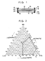
- FIG. 1 We have illustrated in FIG. 1 one of many monolithic ceramic capacitors of like construction fabricated in the subsequent Examples of our invention by way of a preferable embodiment thereof.
- the representative capacitor is shown to have an interlamination of three dielectric ceramic layers 12 and two film electrodes 14.
- the three ceramic layers 12 constitute in combination a solid dielectric body 15 having the low temperature sinterable ceramic compositions in accordance with our invention.
- the capacitor 10 also includes a pair of conductive terminations 16 which are formed on both sides of the dielectric body 15 and which contact the respective film electrodes 14.
- Each termination 16 is shown to comprise a baked on zinc layer 18, a plated on copper layer 20, and a plated on solder layer 22.
- the intermediate one of the three dielectric layers 12 has a thickness of 0.02 millimeter (mm).
- the area of that part of each film electrode 14 which overlaps the other film electrode is 25 mm 2 (5 x 5 mm).
- test capacitors each constructed as shown in FIG. 1, some having their dielectric bodies formulated in accordance with the ceramic compositions of our invention and others not. Then we measured the specific dielectric constant, dielectric loss, resistivity, and temperature dependence of capacitance of the test capacitors. Tables 1 and 2 lists the compositions of the dielectric bodies of all the test capacitors fabricated.
- the ceramic compositions of our invention also include a first additive ingredient consisting of Cr 2 0 3 and / or A1 2 0 3 .
- Table 1 a specifies the amounts, in parts by weight, of the first additive ingredient with respect to 100 parts by weight of the major ingredient.
- the ceramic compositions of our invention furthermore include a second additive ingredient or glass ingredient.
- the second additive ingredient is a additive mixture of B 2 O 3 , Si0 2 and MO or a additive mixture of Li 2 0, Si0 2 and MO.
- Table 1 specifies the amounts, in parts by weight, of the second additive ingredient with respect to 100 parts by weight of the major ingredient.
- Table 2 specifies the relative proportions, in mole percent, of the second additive ingredient B 2 0 3 , Li 2 0, Si0 2 , and MO.
- MO can be any one or more of BaO, MgO, ZnO, SrO and CaO
- Table 2 gives the relative proportions, in mole percent, of these metal oxides.
- the additives of Tests Nos. 1-103 consist of Li 2 0, Si0 2 and MO
- the additive of Tests Nos. 104-140 consist of B 2 0 3 , Si0 2 and MO.
- One hundred parts by weight of this major ingredient was admixed with 0.1 parts by weight of a first additive or Cr 2 O 3 , and 2.0 parts by weight of a second additive of one mole percent Li 2 0, 80 mole percent Si0 2 and 19 mole percent MO.
- the MO was a mixture of 20 mole percent BaO, 20 mole percent SrO, 20 mole percent CaO, 20 mole percent MgO and 20 mole percent ZnO.
- start materials had all purities of not less than 99.0 percent.
- the above specified weights of the start materials do not include those of the impurities contained.
- the desired additive mixture of one mole percent Li 2 0, 80 mole percent Si0 2 and 19 mole percent MO, with the MO consisting of 3.8 mole percent BaO, 3.8 mole percent SrO, 3.8 mole percent CaO, 3.8 mole percent MgO and 3.8 mole percent ZnO.
- the relative proportions of BaO, SrO, CaO, MgO and ZnO were 20 mole percent respectively.
- the dichromium trioxide powder has an average particle size of 0.5 micromiters.
- Tests Nos. 2-140 we made similar capacitors through the same procedure as set forth in the foregoing in connection with the Test No. 1 composition, except for the temperature of sintering in the reductive atmosphere, to which we will presently refer in more detail.
- each test capacitor was first measured at a temperature of 20 degrees C., a frequency of one kilohertz, and an effective voltage of 1.0 volt. Then the specific dielectric constant was computed from the measured value of capacitance, and the area (25 square millimeters) of each of the opposed parts of the film electrodes 14, and the thickness (0.02 millimeter) of that ceramic layer 12 which intervenes between the film electrodes.
- the dielectric loss was measured under the same conditions as the specific constant.
- Resistance between the pair of conductive terminations 16 of each test capacitor was measured after the application of a direct voltage of 100 volts for one minute. Then the resistivity was computed from the measured resistance value and the size of each test capacitor.
- test capacitors were introduced into a thermostatic oven, and their capacitances at various preselected temperatures were measured at a frequency of one kilohertz and an effective voltage of 1.0 volt. Then the percent changes of the capacitances at -55 degrees and + 125 degrees C. from those at 25 degrees C., and at -25 degrees and +85 degrees C. from those at 20 degrees C ., were computed.
- Table 3 gives the properties of the test capacitors as measured by the above described methods, as well as the maximum temperatures at which the test capacitors were sintered in the reductive atmosphere during their manufacture.
- Table 3 gives the percent variations of capacitances only at -55 degrees, + 125 degrees, -25 degrees and +85 degrees C.
- the capacitance variations of all the test capacitors in accordance with our invention were within plus and minus 10 percent in the temperature range of -25 degrees to +8 5 degrees C. and within plus and minus 15 percent in the temperature range of -55 degrees to + 125 degrees C.
- Tests Nos. 52, 53, 62, 70, 71, 72, and 73 compositions had the value of X set at 0.06.
- the capital M in the formula of the major ingredient represents either or both of Ca and Sr as aforesaid.
- the Tests indicate that the use of either or both of Ca and Sr does not substantially affect the characteristics of the resulting capacitors, and that the value of X can be in the range of 0.01 to 0:05 in either case.
- the ceramic compositions of Tests Nos. 85 and 96 contained no the first additive ingredient (Cr 2 0 3 /AI 2 0 3 ). In the resulting capacitors the capacitance variation at -55 degrees C. was outside the desired range of plus and minus 15 percent, and the capacitance variation at -25 degrees C. was outside the desired range of plus and minus 10 percent.
- the ceramic compositions of Tests Nos. 86, 87, 97, and 98 contained 0.01 part by weight of the first additive ingredient with respect to 100 parts by weight of the major ingredient. They possessed the desired electrical characteristics. We set, therefore, the lower limit of the possible proportions of the first additive ingredient at 0.01 part by weight with respect to 100 parts by weight of the major ingredient.
- the Tests Nos. 94, 95, 102 and 103 ceramic compositions contained as much as three parts by weight of the first additive ingredient with respect to 100 parts by weight of the major ingredient.
- the dielectric bodies formulated accorddingly were not coherently bonded on firing at a temperature as high as 1250 degrees C.
- the ceramic compositions of Tests Nos. 91, 93, 99, and 101 contained 3.00 part by weight of the first additive ingredient with respect to 100 parts by weight of the major ingerdient. They possessed the desired electrical characteristics. We set, therefore, the upper limit of the possible proportions of the first additive ingredient at three parts by weight with respect to 100 parts by weight of the major ingredient.
- the first additive ingredient is either or both of Cr 2 0 3 and AI 2 O 3 as aforesaid.
- the Tests indicate that the use of either or both of Cr 2 0 3 and Al 2 O 3 does not substnatially affect the characteristics of the resulting capacitors, and that the weight part of the first additive ingredient can be in the range of 0.01 to 3.0 in the either case.
- the addition of the first additive ingredient (Cr 2 O 3 / Al 2 O 3 ) to the compositions improves the temperature dependence of capacitance.
- the first additive ingredient serves to make the capacitors that the capacitance variation is from -15 % to + 15 % in a temperature range of -55 degrees to + 125 degrees C., and from -10 % to + 10 % in a temperature range of -25 degrees to +85 degrees C.
- the first additive ingredient serves to make the dielectric bodies with a high resistivity.
- the ceramic compositions of Tests Nos. 27, 33, 39, 129 and 135 contained no the second additive ingredient specified by our invention.
- the dielectric bodies formulated accordingly were not coherently bonded on firing at a temperature as high as 1250 degrees C.
- the ceramic compositions of Tests Nos. 28, 34, 40, 130 and 136 contained 0.2 part by weight of the second additive ingredient with respect to 100 parts by weight of the major ingredient.
- the firing temperatures for these test capacitors were as low as 1190 degrees C., they possessed the desired electrical characteristics.
- the tests Nos. 32, 38, 44, 134 and 140 ceramic compositions contained six parts by weight of the second additive ingredient with respect to 100 parts by weight of the major ingredient.
- the specific dielectric constants of the resulting capacitors were less than the above established criterion of 3000. Also, their capacitance variations were outside the range of plus and minus 10 percent at -25 degrees or +85 degrees C. or outside the range of plus and minus 15 percent at -55 degrees or + 125 degrees C.
- the proportion of the second additive ingredient was reduced to five parts by weight as in Tests Nos. 31, 37, 43, 133 and 139, the resulting capacitors had all the desired electrical characteristics. Accordingly, the upper limit of the possible proportions of the second additive ingredient is set at five parts by weight with respect to 100 parts by weight of the major ingredient.
- the point A in the ternary diagram indicates the Test No. 1 additive composition of one mole percent LizO, 80 mole percent Si0 2 , and 19 mole percent MO.
- the point B indicates the Test No. 2 additive composition of one mole percent Li 2 0, 39 mole percent SiO 2 , and 60 mole percent MO.
- the point C indicates the Test No. 3 additive composition of 30 mole percent LizO, 30 mole percent SiOz, and 40 mole percent MO.
- the point D indicates the Test No.
- the relative proportions of the additives Li 2 0, Si0 2 , and MO of the ceramic compositions in accordance with our invention are within the region bounded by the lines sequentially connecting the above defined points A, B, C, D and E in the ternary diagram of FIG. 2.
- Tables 1, 2 and 3 prove that the second additive compositions within the above defined region makes possible the provision of capacitors of the desired characteristics.
- the second additive compositions of Tests Nos. 11-16 all fall outside that region, and the corresponding dielectric bodies were not coherently bonded on firing at a temperature of as high as 1250 degrees C.
- the above specified acceptable range of the relative proportions of the second additives holds true regardless of whether only one of BaO, MgO, ZnO, SrO and CaO is employed as MO, as in Tests Nos. 22-26, or two or more or all of them are employed as in the other Tests.
- the acceptable range of the relative proportions of B 2 O 3 , SiO 2 and MO, the second additive ingredient of the ceramic compositions in accordance with our invention can be definitely stated in reference to the ternary diagram of FIG. 3.
- the point A in the ternary diagram indicates the Test No. 104 additive composition of one mole percent B 2 0 3 , 80 mole percent Si0 2 , and 19 mole percent MO.
- the point B indicates the Test No. 105 additive composition of one mole percent B 2 0 3 , 39 mole percent SiO z , and 60 mole percent MO.
- the point C indicates the Test No.
- the point D indicates the Test No. 107 additive composition of 90 mole percent B 2 0 3 , 1 mole percent Si0 2 , and 9 mole percent MO.
- the point E indicates the Test No. 108 additive composition of 90 mole percent B 2 0 3 , 9 mole percent Si0 2 , and 1 mole percent MO.
- the point F indicates the Test No. 109 additive composition of 19 mole percent 6 2 0 3 , 80 mole percent Si0 2 , and 1 mole percent MO.
- the relative proportions of the additives 6 2 0 3 , Si0 2 and MO of the ceramic compositions in accordance with our invention are within the region bounded by the lines sequentially connecting the above defined points A, B, C, D, E and F in the ternary diagram of FIG. 3.
- Tables 1, 2 and 3 prove that the second additive compositions within the above defined region makes possible the provision of capacitors of the desired characteristics.
- the second additive compositions of Tests Nos. 110-113 all fall outside that region, and the corresponding dielectric bodies were not coherently bonded on firing at a temperature of as high as 1250 degrees C.
- the above specified acceptable range of the relative proportions of the second additives holds true regardless of whether only one of BaO, MgO, ZnO, SrO and CaO is employed as MO, as in Tests Nos. 120-124, or two or more or all of them are employed as in the other Tests.
Landscapes
- Engineering & Computer Science (AREA)
- Chemical & Material Sciences (AREA)
- Power Engineering (AREA)
- Ceramic Engineering (AREA)
- Manufacturing & Machinery (AREA)
- Microelectronics & Electronic Packaging (AREA)
- Inorganic Chemistry (AREA)
- Materials Engineering (AREA)
- Structural Engineering (AREA)
- Organic Chemistry (AREA)
- Ceramic Capacitors (AREA)
- Compositions Of Oxide Ceramics (AREA)
- Inorganic Insulating Materials (AREA)
Applications Claiming Priority (4)
| Application Number | Priority Date | Filing Date | Title |
|---|---|---|---|
| JP1283710A JPH03145114A (ja) | 1989-10-31 | 1989-10-31 | 磁器コンデンサ及びその製造方法 |
| JP283710/89 | 1989-10-31 | ||
| JP298136/89 | 1989-11-16 | ||
| JP1298136A JPH03159108A (ja) | 1989-11-16 | 1989-11-16 | 磁器コンデンサ及びその製造方法 |
Publications (3)
| Publication Number | Publication Date |
|---|---|
| EP0425971A2 true EP0425971A2 (de) | 1991-05-08 |
| EP0425971A3 EP0425971A3 (en) | 1991-11-27 |
| EP0425971B1 EP0425971B1 (de) | 1994-05-18 |
Family
ID=26555162
Family Applications (1)
| Application Number | Title | Priority Date | Filing Date |
|---|---|---|---|
| EP90120257A Expired - Lifetime EP0425971B1 (de) | 1989-10-31 | 1990-10-22 | Vollisolierter Kondensator und Verfahren zu seiner Herstellung |
Country Status (4)
| Country | Link |
|---|---|
| US (1) | US5051864A (de) |
| EP (1) | EP0425971B1 (de) |
| KR (1) | KR930004741B1 (de) |
| DE (1) | DE69009001T2 (de) |
Cited By (1)
| Publication number | Priority date | Publication date | Assignee | Title |
|---|---|---|---|---|
| EP0782156A2 (de) | 1995-12-12 | 1997-07-02 | Philips Patentverwaltung GmbH | Vielschichtkondensator mit Dielektrikum aus modifiziertem Bariumstrontiumtitanat |
Families Citing this family (3)
| Publication number | Priority date | Publication date | Assignee | Title |
|---|---|---|---|---|
| KR100190558B1 (ko) * | 1995-03-04 | 1999-10-15 | 구본준 | 강유전체 및 이를 채용한 반도체장치의 커패시터 |
| JP3344314B2 (ja) * | 1998-04-08 | 2002-11-11 | 株式会社村田製作所 | パルス発生用コンデンサ |
| US20130127174A1 (en) * | 2013-01-15 | 2013-05-23 | Duncan G. Cumming | Method for Generating Tidal Energy Utilizing the Scalar Gravitational Potential of Celestial Bodies |
Family Cites Families (9)
| Publication number | Priority date | Publication date | Assignee | Title |
|---|---|---|---|---|
| DE3476993D1 (en) * | 1983-11-30 | 1989-04-13 | Taiyo Yuden Kk | Low temperature sintered ceramic materials for use in soliddielectric capacitors or the like, and method of manufacture |
| DE3475063D1 (en) * | 1983-11-30 | 1988-12-15 | Taiyo Yuden Kk | Low temperature sinterable ceramic materials for use in solid dielectric capacitors or the like, and method of manufacture |
| JPS60118666A (ja) * | 1983-11-30 | 1985-06-26 | 太陽誘電株式会社 | 誘電体磁器組成物 |
| DE3476653D1 (en) * | 1983-11-30 | 1989-03-16 | Taiyo Yuden Kk | Low temperature sintered ceramic materials for use in solid dielectric capacitors or the like, and method of manufacture |
| JPH0610931B2 (ja) * | 1984-07-05 | 1994-02-09 | 株式会社村田製作所 | 非還元性誘電体磁器組成物 |
| US4801131A (en) * | 1987-10-19 | 1989-01-31 | Bagley Jeffrey W | Work holding device |
| JPH02228018A (ja) * | 1989-02-28 | 1990-09-11 | Taiyo Yuden Co Ltd | 磁器コンデンサ及びその製造方法 |
| JPH02228019A (ja) * | 1989-02-28 | 1990-09-11 | Taiyo Yuden Co Ltd | 磁器コンデンサ及びその製造方法 |
| US4988650A (en) * | 1989-06-23 | 1991-01-29 | Murata Manufacturing Co., Ltd. | Auxiliary agent for sintering ceramic material |
-
1990
- 1990-10-22 EP EP90120257A patent/EP0425971B1/de not_active Expired - Lifetime
- 1990-10-22 US US07/602,105 patent/US5051864A/en not_active Expired - Fee Related
- 1990-10-22 DE DE69009001T patent/DE69009001T2/de not_active Expired - Fee Related
- 1990-10-31 KR KR1019900017531A patent/KR930004741B1/ko not_active Expired - Fee Related
Cited By (2)
| Publication number | Priority date | Publication date | Assignee | Title |
|---|---|---|---|---|
| EP0782156A2 (de) | 1995-12-12 | 1997-07-02 | Philips Patentverwaltung GmbH | Vielschichtkondensator mit Dielektrikum aus modifiziertem Bariumstrontiumtitanat |
| US5790367A (en) * | 1995-12-12 | 1998-08-04 | U.S. Philips Corporation | Multilayer capacitor comprising a dielectric of modified barium strontium titanate |
Also Published As
| Publication number | Publication date |
|---|---|
| DE69009001D1 (de) | 1994-06-23 |
| EP0425971A3 (en) | 1991-11-27 |
| EP0425971B1 (de) | 1994-05-18 |
| KR930004741B1 (ko) | 1993-06-03 |
| US5051864A (en) | 1991-09-24 |
| KR910008758A (ko) | 1991-05-31 |
| DE69009001T2 (de) | 1994-12-01 |
Similar Documents
| Publication | Publication Date | Title |
|---|---|---|
| EP0187960B1 (de) | Bei niedriger Temperatur gesinterter keramischer Kondensator mit hoher Gleichspannungsdurchschlagsfestigkeit und Verfahren zur Herstellung | |
| EP0155365A2 (de) | Keramische Materialien mit niedriger Sintertemperatur für feste dielektrische Kondensatoren und Verfahren zu ihrer Herstellung | |
| EP0155364A2 (de) | Keramische Materialien mit niedriger Sintertemperatur für feste dielektrische Kondensatoren und Verfahren zu ihrer Herstellung | |
| EP0385340B1 (de) | Festdielektrikumkondensator und Herstellungsverfahren | |
| US4700266A (en) | Low temperature sintered ceramic capacitor with a temperature compensating capability, and method of manufacture | |
| EP0224807A2 (de) | Bei niedriger Temperatur gesinterter keramischer Kondensator mit Temperaturkompensationsmöglichkeit und Verfahren zur Herstellung | |
| US4809131A (en) | Low temperature sintered ceramic capacitor having a high resistivity and bending strength, and method of manufacture | |
| US4700265A (en) | Low temperature sintered ceramic capacitor with a temperature compensating capability, and method of manufacture | |
| EP0385339B1 (de) | Festdielektrikumkondensator und Verfahren zu seiner Herstellung | |
| EP0431530B1 (de) | Festdielektrikumkondensator und Verfahren zur Herstellung | |
| US4723193A (en) | Low temperature sintered ceramic capacitor with a temperature compensating capability, and method of manufacture | |
| US4809130A (en) | Low temperature sintered ceramic capacitor having a high resistivity and bending strength, and method of manufacture | |
| EP0385364B1 (de) | Festdielektrikumkondensator und Herstellungsverfahren | |
| EP0385338B1 (de) | Festdielektrikumkondensator und Herstellungsverfahren | |
| EP0425970B1 (de) | Festdielektrikumkondensator und Verfahren zur Herstellung | |
| EP0430178B1 (de) | Festdielektrikum-Kondensator und Verfahren zur Herstellung | |
| EP0385363A2 (de) | Widerstand mit festem Dielektrikum und Verfahren zu seiner Herstellung | |
| EP0430172B1 (de) | Festdielektrikum-Kondensator und Verfahren zur Herstellung | |
| EP0431531B1 (de) | Festdielektrikumkondensator und Verfahren zur Herstellung | |
| EP0430179B1 (de) | Festdielektrikum-Kondensator und Verfahren zur Herstellung | |
| EP0425971B1 (de) | Vollisolierter Kondensator und Verfahren zu seiner Herstellung | |
| EP0431533B1 (de) | Festdielektrikumkondensator und Verfahren zu seiner Herstellung | |
| EP0385365B1 (de) | Festdielektrikumkondensator und Herstellungsverfahren | |
| EP0432418B1 (de) | Festdielektrikumkondensator und Verfahren zur Herstellung | |
| EP0226071B1 (de) | Bei niedriger Temperatur gesinterter keramischer Kondensator mit Temperaturkompensationsmöglichkeit und Verfahren zur Herstellung |
Legal Events
| Date | Code | Title | Description |
|---|---|---|---|
| PUAI | Public reference made under article 153(3) epc to a published international application that has entered the european phase |
Free format text: ORIGINAL CODE: 0009012 |
|
| AK | Designated contracting states |
Kind code of ref document: A2 Designated state(s): DE FR GB |
|
| PUAL | Search report despatched |
Free format text: ORIGINAL CODE: 0009013 |
|
| AK | Designated contracting states |
Kind code of ref document: A3 Designated state(s): DE FR GB |
|
| 17P | Request for examination filed |
Effective date: 19920527 |
|
| 17Q | First examination report despatched |
Effective date: 19930527 |
|
| GRAA | (expected) grant |
Free format text: ORIGINAL CODE: 0009210 |
|
| AK | Designated contracting states |
Kind code of ref document: B1 Designated state(s): DE FR GB |
|
| REF | Corresponds to: |
Ref document number: 69009001 Country of ref document: DE Date of ref document: 19940623 |
|
| ET | Fr: translation filed | ||
| PG25 | Lapsed in a contracting state [announced via postgrant information from national office to epo] |
Ref country code: GB Effective date: 19941022 |
|
| PLBE | No opposition filed within time limit |
Free format text: ORIGINAL CODE: 0009261 |
|
| STAA | Information on the status of an ep patent application or granted ep patent |
Free format text: STATUS: NO OPPOSITION FILED WITHIN TIME LIMIT |
|
| 26N | No opposition filed | ||
| GBPC | Gb: european patent ceased through non-payment of renewal fee |
Effective date: 19941022 |
|
| PG25 | Lapsed in a contracting state [announced via postgrant information from national office to epo] |
Ref country code: FR Effective date: 19950630 |
|
| REG | Reference to a national code |
Ref country code: FR Ref legal event code: ST |
|
| PGFP | Annual fee paid to national office [announced via postgrant information from national office to epo] |
Ref country code: DE Payment date: 19951025 Year of fee payment: 6 |
|
| PG25 | Lapsed in a contracting state [announced via postgrant information from national office to epo] |
Ref country code: DE Effective date: 19970701 |