EP0424979A2 - Adressier-Selektier-System - Google Patents
Adressier-Selektier-System Download PDFInfo
- Publication number
- EP0424979A2 EP0424979A2 EP90121700A EP90121700A EP0424979A2 EP 0424979 A2 EP0424979 A2 EP 0424979A2 EP 90121700 A EP90121700 A EP 90121700A EP 90121700 A EP90121700 A EP 90121700A EP 0424979 A2 EP0424979 A2 EP 0424979A2
- Authority
- EP
- European Patent Office
- Prior art keywords
- module
- link
- chip
- target
- modules
- Prior art date
- Legal status (The legal status is an assumption and is not a legal conclusion. Google has not performed a legal analysis and makes no representation as to the accuracy of the status listed.)
- Withdrawn
Links
- 239000003550 marker Substances 0.000 claims description 7
- 238000012545 processing Methods 0.000 abstract description 3
- 238000000034 method Methods 0.000 description 17
- 238000004891 communication Methods 0.000 description 11
- 238000010586 diagram Methods 0.000 description 10
- 230000006870 function Effects 0.000 description 10
- 239000000872 buffer Substances 0.000 description 7
- 230000008569 process Effects 0.000 description 7
- 238000003491 array Methods 0.000 description 4
- 230000005540 biological transmission Effects 0.000 description 3
- 230000008859 change Effects 0.000 description 3
- 230000000295 complement effect Effects 0.000 description 3
- 238000001514 detection method Methods 0.000 description 3
- 230000008901 benefit Effects 0.000 description 2
- 230000002950 deficient Effects 0.000 description 2
- 238000005516 engineering process Methods 0.000 description 2
- 230000001788 irregular Effects 0.000 description 2
- 238000013507 mapping Methods 0.000 description 2
- 230000002093 peripheral effect Effects 0.000 description 2
- 230000002457 bidirectional effect Effects 0.000 description 1
- 230000003139 buffering effect Effects 0.000 description 1
- 230000001186 cumulative effect Effects 0.000 description 1
- 238000013500 data storage Methods 0.000 description 1
- 230000001934 delay Effects 0.000 description 1
- 230000001419 dependent effect Effects 0.000 description 1
- 230000008030 elimination Effects 0.000 description 1
- 238000003379 elimination reaction Methods 0.000 description 1
- 230000010354 integration Effects 0.000 description 1
- 230000007246 mechanism Effects 0.000 description 1
- 239000004065 semiconductor Substances 0.000 description 1
- 230000011664 signaling Effects 0.000 description 1
- 230000003068 static effect Effects 0.000 description 1
- 238000012546 transfer Methods 0.000 description 1
- 238000013519 translation Methods 0.000 description 1
- 230000001960 triggered effect Effects 0.000 description 1
Images


Classifications
-
- G—PHYSICS
- G11—INFORMATION STORAGE
- G11C—STATIC STORES
- G11C29/00—Checking stores for correct operation ; Subsequent repair; Testing stores during standby or offline operation
- G11C29/006—Checking stores for correct operation ; Subsequent repair; Testing stores during standby or offline operation at wafer scale level, i.e. wafer scale integration [WSI]
Definitions
- the present invention relates to a random address system for an array of circuit modules which include configuration logic enabling the modules to be connected in a chain leading from a start or entry module to a target module.
- the invention is concerned more specifically with a system as defined in the pre-characterizing part of claim 1.
- the modules may be part of a wafer scale integrated (WSI) circuit, or as sub-wafer-scale integrated circuit.
- WSI wafer scale integrated
- each module includes a function unit which performs the function proper of the module.
- GB 1 377 859 describes how circuit modules may be undiced chip areas of an integrated circuit wafer and a chain of modules may be grown by actuation of electronic switching functions within the modules. It is also proposed in GB 2 114 782 to store the sequence of commands necessary to set up a chain of good modules, preferably permanently in a PROM, and to set up the chain rapidly in accordance with the stored commands, whenever the device is switched on.
- a simple form of control logic using only a single global command line is described in our International patent application published as WO87/00675.
- EP 0146275 discloses a system for communicating between a plurality of transmitters and receivers via a network of distributors and concentrators.
- the distributors have one input and two outputs each and one of the outputs is selected in dependence upon the first bit of a routing message received by that distributor.
- the concentrators have two inputs and one output and accept an input signal from either input and disable the other input for the duration of the signal.
- different types of modules are used for the transmitters and receivers and for the distributors.
- Distributors are not capable of acting as transmitters or receivers.
- each transmitter/receiver station communicates via an access node built up from a plurality of distributors and concentrators.
- the access nodes are linked by two closed communication loops which carry signals in opposite directions so that any transmitter/receiver station can communicate with any other station in either direction round the loop.
- Each loop is moreover bidirectional.
- Another embodiment uses a network of nodes between a group of transmitter stations and a group of receiver stations.
- a system implementing the proposals of the document cited in the preceding paragraph and in accordance with the pre-characterizing part of claim 1 is disclosed in US-A 4 020 469.
- the controller sends a stream of data comprising groups of serial bits. Each group includes two bits selecting the next module and other bits which establish a functional state for the current module. The groups are stripped off module by module.
- the data stream is used to load a functional state of the complete array which, when fully loaded, constitutes a kind of software-defined logic array, set up with its processing digital circuits set up to perform processing functions.
- the present invention on the other hand relates to a technique for forming a chain of modules whenever a module is accessed.
- This has been proposed in our pending International Patent Application PCT/GB86/00601, unpublished at the date of filing the present application, using an extension of the technique in WO87/00675 and requiring a global command line. Rapid operation requires a significantly more efficient addressing.
- the object of this invention is to meet this need and to allow rapid random access to any one target module.
- the invention is defined in claim 1.
- the target module is target-addressed
- the preceding modules in the chain are link-addressed.
- the invention contemplates sending the address commands for all modules required to form a chain as a single address string, comprising a packet or group of bits for each addressed module.
- Each link-addressed module responds to its own group of bits to link on to the next module and sends on the string with that group stripped off.
- each module has four neighbours to which it can connect, two bits suffice to identify which module to link to, i.e. each group of bits can be a di-bit.
- To add information to identify the target-addressed module would require a third bit, a 50% overhead.
- a preferred solution in the case of bit-serial operation is for a module to regard itself as target-addressed when the group of bits which it receives tells it to link on to what is the preceding module already in the chain.
- the end of the string may be marked by a single bit or other specific pattern no larger than one of the groups of bits.
- a module regards itself as target-addressed when the string which it receives has the specific pattern at the most significant position and is otherwise null.
- the target module may relay a chip-select signal to its function unit.
- the invention provides a means of addressing and accessing random chips with minimum delay in a WSI application. It provides benefits for the random access of data storage chips from outside the wafer.
- all chip addressing is achieved through the data highway. No timing or synchronisation information need be distributed globally. Thus high speed communications are possible because no global timing constraints apply.
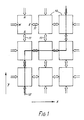
- Fig. 1 shows part of a WSI array of modules 10.
- the array in this example is rectangular and each module or chip 10 can be regarded as having four sides N, S, E, W (North, South, East, West) and corresponding nearest neighbour modules. Nearest neighbour modules are connected by sets of lines 11 which make it possible to establish a chain of linked chips, e.g, the chain denoted by a heavy line 12.
- the chains leading to all possible target chips from a common start chip form an irregular tree structure, with no crossing paths. Only one path at a time can be set up from the start chip.
- Each chip includes both a function unit, e.g. a dynamic RAM and configuration logic which enables the chains to be set up.
- the chips may be identified in the array by their X and Y coordinate numbers. Once a chain is set up, its chips can be regarded as a series of chips A, B, C etc. as shown in Fig. 2.
- the main chip-to-chip connections are those shown, namely a forward or transmit serial data line XMIT and a chip-select line CS.
- a return or receive data line REC is provided in the preferred embodiment.
- Each chip receives a clock signal CLK which may be distributed globally to all chips on the wafer or be relayed only down the chain of chips, like CS. Unlike the data paths, all clock paths stay set up and exist simultaneously once configured.
- the number of nodes in a clock path chain is relatively small, minimising any distortion to the clock signal.
- Each chip (X, Y) is assigned a unique address string which defines the minimum length path for access through a chain of chips with nearest-neighbour, interchip communication.
- the address is a coded series of directional instructions which define the successive links which must be formed between all intermediate chips to configure the path to the target-addressed chip.
- Configuration of available chips on the wafer is efficient. A path can be mapped to all chips not trapped by chips whose configuration logic is defective.
- a new path is configured by transmission of a single address string at the entry chip A on the wafer.
- Each chip in the path in turn strips off the first two bits at the head of the address string it receives to determine the direction of the next chip in the chain, and then treats all following bits as data to be passed on to the next selected chip.
- Fig. 3 shows the clock signal CLK, CS as asserted at chip A, the address string XMITA applied to chip A and so on.
- XMITA comprises di-bits A0, A1: B0, B1; C0, C1 whereas XMITB comprises only B0, B1 and C0, C1, while XMITC comprises C0, C1 only.
- the waveforms XMITA etc. in Fig. 3 identify the relevant bit periods, not the actual di-bit values.
- the target-addressed chip is identified by setting its exit direction to coincide with its entry direction. This loop-back condition signals to a chip that it has been addressed to receive or transmit data.
- a configured path is maintained by the presence of the static chip-select signal CS which passes along the chain of chips forming the path ( Figures 2 and 3).
- a path is de-configured by de-asserting CS at the entry chip, and allowing the change to ripple along the configured chain of chips.
- CS need only be de-asserted for a single clock cycle to initiate de-configuration of an existing path, before it is re-asserted to configure a path to a new target-addressed chip.
- the short chip access time permits a handshake to be incorporated into data transmission, allowing a communication path to be verified before data is passed. This gives greater security of data communication due to closed loop operation.
- the wafer Because the required commnunication path is set up for each chip access, the wafer is not susceptible to interruption of a path by noise in a quiescent period, and any interruption of a path during a chip access has no repercussions on chips other than the one being accessed.
- An instruction can be broadcast to all chips along a path by having each chip recognise the address termination loop-back condition as it is passed to the next chip in the chain, then consider the following preset number of bits as an instruction. This provides an effective means of broadcasting instructions such as refresh.
- Multiple entry points to a wafer may be provided, and separate paths configured to provide simultaneous access to several chips. It must be ensured that multiple paths never cross.
- the ability to separately reconfigure the multiple paths on a wafer allows data to be communicated with multiple bit widths, with external buffers maintaining synchronisation between data bits. This synchronisation is made necessary by the use of imperfect memory arrays, with the result that boundaries between blocks and chips will occur at different times for different bits of the data word. The short latency in accessing any chip on the wafer minimises the length of buffer which must be used to maintain this synchronisation.
- the address string which is transmitted is in the form of coded directional information defining a direct path to the chip to be accessed. It comprises a series of two-bit packets of data, each of which defines one of four possible directions to be taken in forming the link between two successive chips in the chain. Each chip in the chain strips off the first two bits from the string it receives and uses them to determine which of its four neighbours should become the next chip in the chain. It then considers all subsquent bits of the string as data to be passed to the next chip thus set up.
- the principle may be extended to chips with more than four logical neighbours and data packets with more than two bits.
- Figure 3 shows that a selected chip in the chain is alerted by the assertion of its Chip Select (CS) line, which subsequently remains asserted for as long as the configured path is to be maintained. Following a one cycle delay, two bits of data are received on the Transmit (XMIT) input which indicate the required output direction to the next chip in the chain. A CS output signal is immediately generated and passed to the next chip thus identified, followed by the remainder of the address string after a single cycle delay.
- CS Chip Select
- the total delay in configuring a new path is three clock cycles for each link in the chain which must be formed.
- a configured path is deleted by de-assertion of the CS signal to the first chip in the chain. This change ripples along the chain with one cycle delay per chip, breaking all configured links.
- a chip is identified as the addressed chip to be accessed by the device of defining the output direction from the chip to be the same as its input direction. This is achieved by setting the final direction code in the address string to be the exclusive-OR function of the penultimate code, indicating a loop-back condition. This is interpreted by the final chip in the chain as a selection for access.
- Fig. 4 shows the chip interconnection signals of a module 10.
- Each side of the chip has a connection XMITin; these four connections are commonly connected within the chip.
- the corresponding outputs XMITout(N) etc. are individual to the sides of the chip.
- Input connections RECin(N) etc. are individual to the sides of the chip whereas RECout is common.
- CSin(N) etc. and CSout(N) etc. are both individual to the sides.
- CLKinis common and CLKout(N) etc. are individual to the sides.
- Fig. 5 shows the configuration logic together with the user circuits 14 whose precise nature forms no part of the present invention. It will be seen that these circuits have serial data in and data out terminals, a chip-enable terminal and a clock terminal. There are many known ciruits with such connections.
- the user circuits could be dynamic RAM circuits substantially as described in WO87/00675 for example.
- D-type flip-flops and gates are shown, some in heavy lines. These are individual to the chip sides, i.e. the set of devices shown in heavy lines in replicated four times to provide a set for each side N, S, E and W. References for these lines conclude with the characters (D) where 'D' stands for direction and may be N, S, E or W.
- D the characters
- 'D' stands for direction and may be N, S, E or W.
- the devices shown in ordinary lines are common to all sides. Connections will not be described; they are clear from the drawing.
- flip-flop 15(D) When a chip is accessed from a given side, CS true is latched in a corresponding flip-flop 15(D) and data on XMITin is buffered in a flip-flop 16 and also passed to three cascaded flip-flops 17, 18 and 19 which have been respectively preset, cleared and cleared, via an OR gate 29, so long as flip-flop 15(D) remains clear.
- flip-flops 17 and 18 After two clock cycles flip-flops 17 and 18 contain the first two bits of the address string arriving on XMITin and the flip-flop 19 contains the '1' bit preset in flip-flop 17. This state of the flip-flops is frozen because an AND gate 20 is then disabled by flip-flop 19 to remove the clock signal from the three flip-flops.
- a decoder 21 decodes the di-bit in flip-flops 17 and 18 to a direction signal N, S, E, or W denoting the exit direction from the chip.
- the decode is to some extent arbitrary but the di-bits for N and S are complementary and the di-bits for E and W are also complementary.
- An AND gate 22(D) corresponding to the decode is enabled by the set flip-flop 19 and provides an enabling signal to two AND gates 23(D) and 24(D). Which of these gates provides a true output depends upon the state of the CS flip-flop 15(D). The two situations are as follows:-
- the gated N, S, E or W signal from the gate 22(D) sets a corresponding flip-flop 34(D) which enables an AND gate 33(D) to pass CLKin to CLKout(N), (S), (E) or (W) in correspondence with the selected exit direction.
- the set flip-flop 34(D) remains set until the wafer is switched off.
- Figure 6 shows a hypothetical wafer with random defective chips resulting in a yield of 75%. Only the simple logic shown in Figure 5 need function to allow a chip to be incorporated in a chain, and so this yield is very conservative for a practical case.
- the hypothetical wafer contains a total of 316 dice, which is representative of a practical case.
- a simple wavefront mapping algorithm is employed to plot and record a direct path to all accessible chips on the wafer.
- the paths to all accessible and unmapped chips adjacent to the start chip are determined by trying to create all possible links from this chip.
- the paths thus formed have only one link, and the mapped chips are labelled 1 in Figure 6.
- the process is repeated by attempting to access all unmapped chips adjacent to the chips labelled 1, to form all two-link paths to the chips labelled 2.
- paths to chips ahead of the advancing wave front of mapped chips are determined by the simple addition of a new link direction to the address strings already stored.
- Figure 6 shows the positions of chips on the wavefront after 1 to 5 and 11 iterations of this process.
- the routes of paths to all accessible chips on a wafer form an irregular tree structure whose root is the entry chips to the wafer.
- the mapped path to chip (10,4) requires three links to be made to the North, so that the address string required to access this chip is NNNS.
- the address string is thus 00000011 if the di-bits are assigned as indicated above.
- the path to chip (12.3) has a required address string NEENS.
- FIG. 7 shows the routes of paths to chips (2.6), (2.15), (8.20), (13.20), (19.15) and (19.6), by way of example. Note that only one of these paths can be configured at any time.
- the wafer of Fig.6 has a maximum path length of 24 links, and a median path length of 14 links. With 75% chip yield as shown, the wafer has a maximum path length of 28, still with a median of 14.,
- the median access time of a chip on the wafer is 42 clock cycles, or 2.1 microseconds if a 20 megahertz clock frequency is assumed.
- the time required to configure a path and transmit an instruction to every chip on the wafer is 664 microseconds. This would be the overhead required to initiate a refresh on dynamic RAM chips, for example.
- an instruction can be transmitted to every chip on the wafer by configuring paths only to the chips on the periphery, and using the broadcast facility to the intermediate chips along the paths. Since there are only 56 peripheral chips, an instruction can be transmitted to every chip in 118 microseconds.
- the path configured for instruction broadcast need not be a direct path to a target chip, but could be arranged to be a meandering path to include a larger number of chips, for example, a spiral path. An embodiment of the invention with the broadcast facility is described below.
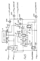
- Fig. 8 shows a block diagram of the logic required to generate and control the chip address string and to interface the wafer to an electronic system.
- the address string required to access each chip is stored in successive bytes in a ROM 35 the number of bytes required being dependent on the length of the path to the chip and hence the length of the address string.
- Each chip on the wafer is allocated one of a sequential series of identification numbers, and this chip number is used to define the most significant group of bits of the ROM address input.
- the least significant address bits are controlled from a byte counter 36, which is incremented to address the successive bytes of the address string.
- Successive bytes of the address string are loaded into a shift register 37 and shifted to the wafer XMIT input, until a loop-back condition of direction codes is detected by a detector 39. This indicates the end of the address string and causes data to be switched to XMIT line via a multiplexer 38.
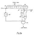
- Fig. 8A shows the shift register 37 and the loop back detector 39.
- the shift register comprises eight stages which are parallel-loaded from the ROM 35, including a stage 40 towards the least-significant end, which is the stage from which the address string passes out to the multiplexer 38.
- the register further comprises another three less significant stages 41.
- Two exclusive OR gates 42 and an AND gate 43 detect when the di-bit with its less-significant bit in stage 40 is complementary to the di-bit in the two least-significant of the stages 41.
- the gate 43 provides a signal to a sequencer 44 and is enabled only in even clock periods by a divide by two counter stage 49.
- the sequencer provides overall control of the system and in particular responds to a signal 45 from the computer commanding the system as a peripheral to initiate addressing a target chip, signals back to the computer on line 46 when the address string has been sent out, asserts CS at the entry chip until commanded by the computer to clear down the chip chain, and responds to the loop back detection signal to switch over the multiplexer 38 to transmit data from the computer. It also clears and increments to the byte counter 36.
- Refresh of dynamic RAM chips on the wafer may be controlled by multiplexing to the ROM address input a chip number from a chip refresh counter 47, in order to initiate refresh cycles in the chips in preset order in a regular cycle. Refresh may be initiated in bursts or all chips may be triggered in one operation.
- the sequencer 44 controls both the refresh counter 47 and a multiplexer 48 which selects between the chip number provided by the counter and the chip number to a target chip input by the computer.
- the sequencer also increments the byte counter 36 after every eight bits shifted out of the register 37, so long as the loop-back detection signal has not been provided.
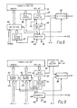
- Figure 9 shows the logic diagram of an alternative method of storing and generating the chip address string.
- the ROM 50 stores for each chip only the two bit direction code defining the link to the preceding chip in the chain.
- the chip number is not one of a sequential series but is formed by separate numbers indicating X and Y coordinates on the chip grid on the wafer.
- Target chip X and Y coordinates from the computer are loaded into up/down counters 51 and 62 which address the ROM, and the two bit code read from ROM is loaded into a shift register 53 to be interpreted to control increment or decrement of the counters to point to the preceding chip in the chain. This process is repeated until the counters point to the start chip, i.e. both counters signal zero contents back to the sequencer.
- Another shift register 54 is used to buffer the address string being constructed.
- the address string is finally shifted out to the XMIT line, to be followed by data.
- This method uses less ROM storage than the first described above, but takes longer to address a chip on the wafer because of the buffering required to reverse the order of the address string.
- Direction interpretation is effected by a circuit 55 which decodes the link directions and then enables only one counter to be counted up or down by one. For example, if the link direction is N, the preceding chip is to the South of the current chip. The counter 51 must stay unchanged but the Y counter 52 must be decremented. The sequencer 44 provides the various timing (clock) signals CK provided to the shift registers 53, 54 and counters 51, 52.
- the techniques described previously can be extended to include an asynchronous communications scheme to allow immediate random access of chips within a wafer scale device.
- the technique is based on the same technique of accessing a chip by a coded address defining the most direct path to that chip, but the address is presented in parallel rather than serial. Access to the chip is therefore within a single operating cycle since there is no pipelining of address and data.
- sub-wafer-scale integration is defined as a multi-chip module of a size less than that of a complete wafer, with a wafer comprising several such modules which can be individually diced.
- This technique is particularly applicable to random access memory modules which act as high capacity memory "superchips" formed from memory chips of lower capacity.
- the access time can be minimised if a high-speed semiconductor technology can be utilised for the communications paths. This can be achieved through the use of Bipolar or BiCMOS memory technologies.
- Fig. 10 The principle of linking chips to form a communication path to the chip being addressed is illustrated in Fig. 10.
- An address string in the form of coded directional information defining a direct path to the chip being accessed is presented in parallel to the first chip.
- Each input in Fig. 10 represents a di-bit code defining the direction (N, S, E or W) of a link in the communications chain.
- the most significant two bits are used by a direction decoder 60 to determine the direction of the second chip, and the address string is passed on after a di-bit shift, by direction select logic 61.
- the two least significant bits passed on are set to logical zero. This process continues at each successive chip in the chain.
- Fig. 11b shows the string when it has reached the target chip. The marker bit is now in the most significant position; all other bits are zero. This tells the chip that it is target-addressed, rather than link-addressed.
- Fig. 12 shows the configuration logic specifically for the E side of the chip. Elements specific to this direction are shown in heavy lines.
- the chip interconnection signals for the E side are as follows: IN CSin (common to all sides) Ain,N-1 to Ain,0 for the N bits of the address string (common to all sides) XMITin (common to all sides) RECin(E) OUT CSout(E) Aout,N-1(E) to Aout,0(E) XMITout(E) RECout (common to all sides)
- the lines Ain,N-1 to Ain,0 are all connected to a chip select decoder 63 which detects the target addressed string of Fig. 11B and then provides CHIP ENABLE to the user circuit 14.
- the direction decoder 60 decodes Ain,N-1 and Ain,N-2 to provide an exit direction selection signal N, S, E, or W but only when it is (a) enabled by the presence of CS from a preceding chip and (b) not disabled by CHIP ENABLE from the decoder 63.
- Gate 64 which passes CSin as CSout(E).
- Gates 65 (N-2 gates) which pass Ain,N-3 to Ain,0 as Aout, N-1(E) to Aout,2(E) respectively.
- Gates 66 which pass logic '0' as Aout,1(E) and Aout,0(E).
- Gate 67 which passes XMITin as XMITout(E).
- Gate 68 which passes RECin(E) as RECout.
- a memory system formed from a plurality of multi-chip arrays 70 is shown in Fig.13.
- the arrays share common address, data and control inputs, with individual Chip Select lines 71 to select a unique array.
- the address string defining the access route within an array is designated as the Chip Address Link Code and is contained in the Chip Address Translation ROM 72. This string will differ from array to array and the ROM 72 is therefore addressed both by the chip address and the array address. The latter is decoded by a decoder 73 to provide CS to the selected array.
- the Chip Address Link Code is passed by an N-bit bus 74 to Ain,N-1 to Ain,0 of the entry chip of all arrays 70.
- a data and control bus 75 includes the XMIT and REC lines, power supply lines and such other global signal as are required, e.g. RAS, CAS and WE if the user circuits 14 are DRAM's.
- bit address bus 76 conveys a K-bit bit address to every chip for addressing the bit to be written to on XMIT or read from on REC.
- Figs. 10 to 13 is a serial path separate from the parallel path for addressing the chips, it would be possible to use the parallel path for data transfer also, by analogy with Fig.5 which uses the same serial path for addressing and data.
- Fig. 14 shows the format of a broadcast instruction, for the serial embodiment of Fig. 5. This commences with LINK1... LINKk... LINKn..., where each LINK is a di-bit code for linking on to the next chip. LINKn links to the target-addressed chip and is therefore followed by the LOOP BACK di-bit which commands the target-addressed chip to use an exit direction back to the chip from which the target-addressed chip was entered. LOOP BACK is immediately followed by a plurality of INSTRUCTION bits and optionally by DATA for a write instruction. The number of INSTRUCTION bits is fixed and may be just two bits in a simple embodiment.
- Chip k in the chain will receive a data stream commencing with the LINKk code, as described previously. All chips in the chain can identify the instruction code by searching for the loop-back condition in the XMITin data stream, and then interpreting the following preset number of bits as an instruction.
- the instruction field can define both broadcast instructions to be executed by all chips in the chain, and target instructions to be executed only by the target addressed chip.
- Fig. 15 shows the logic which implements the broadcast facility. This logic is additional to that shown in Fig. 5.
- the loop-back code is detected by a chain of five flip-flops 80 to 84 of which the first is preset so long as CS is false and the remainder are cleared.
- CS at the output of the OR gate 29 in Fig. 5
- the incoming bit-stream on XMITin is clocked into the chain of flip-flops.
- the preset bit which starts in the flip-flop 80 reaches the flip-flop 84, the first two di-bits are in the flip-flops 80 to 83 and it is appropriate to start looking for the loop back code.
- the flip-flop 84 provides a first of four required enabling inputs to an AND gate 86 which is the loop-back detection gate.
- the second enabling input is provided by a flip-flop 87 connected to divide CK by two and provide its enabling input to the gate 86 only in those clock cycles in which there is one di-bit in flip-flops 80 and 81 and another di-bit in flip-flops 82 and 83, (not in those cycles in which a di-bit is in flip-flops 81 and 82).
- the remaining enabling inputs are provided by two EXCLUSIVE OR gates 88 and 89 which detect when the di-bit in flip-flops 80 and 81 is the exclusive or of that in the flip-flops 82 and 83, i.e., the di-bit in 80, 81 is the LOOP BACK code of LINKn in 82, 83.
- the clock signal CK is removed from the flip-flops 80 to 83 and 87 by an inverter 90 and an AND gate 91.
- the output of the gate 86 thus freezes true. So long as this output had remained false another chain of three flip-flops 92, 93, 94 was held preset, clear, clear, thus putting a marker bit in the first flip-flop 92.
- the ensuing instruction bits are now clocked into the flip-flops 92 and 93 and the marker bit is clocked into the flip-flop 94, whereupon the clock signal CK is removed from all three flip-flops by a gate 95.
- the three flip-flops now respectively provide instruction bit 1, instruction bit 0 and instruction flag. These three bits are furnished to the user circuits 14 (Fig. 5) which decode the two instruction bits when the instruction flag is true.
- the four possibilities with just two instruction bits may be decoded as NOP (00), refresh, read and write and the user circuits 14 (dynamic RAM) may be configured so that they always obey refresh (i.e., whether target-addressed or link-addressed) but obey read and write only in the presence of CHIP ENABLE from the gate 30 in Fig. 5, i.e., when target-addressed. Only refresh is then a broadcast instruction.
- NOP 00
- refresh i.e., whether target-addressed or link-addressed
- CHIP ENABLE i.e., when target-addressed. Only refresh is then a broadcast instruction.
- Fig. 15 can readily be extended to handle longer instruction fields by adding the appropriate number of flip-flops in the chain between flip-flop 93 and flip-flop 94.
Landscapes
- Dram (AREA)
Priority Applications (1)
| Application Number | Priority Date | Filing Date | Title |
|---|---|---|---|
| EP19900121700 EP0424979A3 (en) | 1986-03-18 | 1987-03-18 | Random address system for circuit modules |
Applications Claiming Priority (3)
| Application Number | Priority Date | Filing Date | Title |
|---|---|---|---|
| GB868606695A GB8606695D0 (en) | 1986-03-18 | 1986-03-18 | Random chip addressing algorithm for wsi |
| GB8606695 | 1986-03-18 | ||
| EP19900121700 EP0424979A3 (en) | 1986-03-18 | 1987-03-18 | Random address system for circuit modules |
Related Parent Applications (2)
| Application Number | Title | Priority Date | Filing Date |
|---|---|---|---|
| EP87901599.8 Division | 1987-03-18 | ||
| EP87901599A Division-Into EP0261164B1 (de) | 1986-03-18 | 1987-03-18 | Selektives adressierungssystem für schaltungsmodule |
Publications (2)
| Publication Number | Publication Date |
|---|---|
| EP0424979A2 true EP0424979A2 (de) | 1991-05-02 |
| EP0424979A3 EP0424979A3 (en) | 1991-07-03 |
Family
ID=26125590
Family Applications (1)
| Application Number | Title | Priority Date | Filing Date |
|---|---|---|---|
| EP19900121700 Withdrawn EP0424979A3 (en) | 1986-03-18 | 1987-03-18 | Random address system for circuit modules |
Country Status (1)
| Country | Link |
|---|---|
| EP (1) | EP0424979A3 (de) |
Citations (7)
| Publication number | Priority date | Publication date | Assignee | Title |
|---|---|---|---|---|
| GB1377859A (en) | 1972-08-03 | 1974-12-18 | Catt I | Digital integrated circuits |
| US4020469A (en) | 1975-04-09 | 1977-04-26 | Frank Manning | Programmable arrays |
| GB2114782A (en) | 1981-12-02 | 1983-08-24 | Burroughs Corp | Branched-spiral wafer-scale integrated circuit |
| EP0146275A2 (de) | 1983-12-16 | 1985-06-26 | Gec Plessey Telecommunications Limited | Datenvermittlungssystem |
| WO1987000675A2 (en) | 1985-07-12 | 1987-01-29 | Anamartic Limited | Control system for chained circuit modules |
| WO1987002487A2 (en) | 1985-10-14 | 1987-04-23 | Anamartic Limited | Control system for chained circuit modules |
| EP0261164A1 (de) | 1986-03-18 | 1988-03-30 | Anamartic Ltd | Selektives adressierungssystem für schaltungsmodule. |
Family Cites Families (1)
| Publication number | Priority date | Publication date | Assignee | Title |
|---|---|---|---|---|
| US4443866A (en) * | 1975-08-27 | 1984-04-17 | Corning Glass Works | Automatic device selection circuit |
-
1987
- 1987-03-18 EP EP19900121700 patent/EP0424979A3/en not_active Withdrawn
Patent Citations (7)
| Publication number | Priority date | Publication date | Assignee | Title |
|---|---|---|---|---|
| GB1377859A (en) | 1972-08-03 | 1974-12-18 | Catt I | Digital integrated circuits |
| US4020469A (en) | 1975-04-09 | 1977-04-26 | Frank Manning | Programmable arrays |
| GB2114782A (en) | 1981-12-02 | 1983-08-24 | Burroughs Corp | Branched-spiral wafer-scale integrated circuit |
| EP0146275A2 (de) | 1983-12-16 | 1985-06-26 | Gec Plessey Telecommunications Limited | Datenvermittlungssystem |
| WO1987000675A2 (en) | 1985-07-12 | 1987-01-29 | Anamartic Limited | Control system for chained circuit modules |
| WO1987002487A2 (en) | 1985-10-14 | 1987-04-23 | Anamartic Limited | Control system for chained circuit modules |
| EP0261164A1 (de) | 1986-03-18 | 1988-03-30 | Anamartic Ltd | Selektives adressierungssystem für schaltungsmodule. |
Non-Patent Citations (1)
| Title |
|---|
| IEEE TRANSACTIONS ON COMPUTERS, vol. C-26, no. 6, June 1977 (1977-06-01), pages 536 - 552 |
Also Published As
| Publication number | Publication date |
|---|---|
| EP0424979A3 (en) | 1991-07-03 |
Similar Documents
| Publication | Publication Date | Title |
|---|---|---|
| EP0261164B1 (de) | Selektives adressierungssystem für schaltungsmodule | |
| US5041971A (en) | Memory accessing switch network | |
| US6345334B1 (en) | High speed semiconductor memory device capable of changing data sequence for burst transmission | |
| US5809557A (en) | Memory array comprised of multiple FIFO devices | |
| EP1121759B1 (de) | Seriell-parallel- und parallel-seriell-umwandlungsvorrichtung | |
| EP0187289A2 (de) | Hierarchische Speicheranordnung | |
| CA1147865A (en) | Message interchange system among microprocessors connected by a synchronous transmitting means | |
| JPH0738166B2 (ja) | 多相メモリ配列の読出回路 | |
| US5319596A (en) | Semiconductor memory device employing multi-port RAMs | |
| KR960025044A (ko) | 반도체 집적회로 | |
| US5127002A (en) | Time slot assigner for use in a serial communication system | |
| US6640275B1 (en) | System and method for data transfer between buses having different speeds | |
| EP0673137A1 (de) | Virtueller Verbindungsspeicher | |
| US20010046176A1 (en) | Semiconductor memory device having prefetch operation mode and data transfer method for reducing the number of main data lines | |
| EP0424979A2 (de) | Adressier-Selektier-System | |
| CN1327371C (zh) | 用于在处理器之间传送通用控制信息的方法和装置 | |
| US6445394B1 (en) | Serialized mapped memory configuration for a video graphics chip | |
| KR100275751B1 (ko) | 구조가 간단한 반도체 메모리 장치 | |
| US4164031A (en) | Memory system | |
| US20030152069A1 (en) | Bundling/de-bundling of low frequency digital data streams | |
| WO1999053638A1 (en) | Method and apparatus for interleaving a data stream | |
| US7362650B2 (en) | Memory arrangement having a plurality of RAM chips | |
| JPS6391766A (ja) | 記憶装置アクセス制御方式 | |
| EP0351959A2 (de) | Vielfachkanalsteuerung | |
| SU734695A1 (ru) | Однокристальный микропроцессор |
Legal Events
| Date | Code | Title | Description |
|---|---|---|---|
| PUAI | Public reference made under article 153(3) epc to a published international application that has entered the european phase |
Free format text: ORIGINAL CODE: 0009012 |
|
| 17P | Request for examination filed |
Effective date: 19901221 |
|
| AC | Divisional application: reference to earlier application |
Ref document number: 261164 Country of ref document: EP |
|
| AK | Designated contracting states |
Kind code of ref document: A2 Designated state(s): AT BE CH DE FR GB IT LI LU NL SE |
|
| PUAL | Search report despatched |
Free format text: ORIGINAL CODE: 0009013 |
|
| AK | Designated contracting states |
Kind code of ref document: A3 Designated state(s): AT BE CH DE FR GB IT LI LU NL SE |
|
| STAA | Information on the status of an ep patent application or granted ep patent |
Free format text: STATUS: THE APPLICATION IS DEEMED TO BE WITHDRAWN |
|
| 18D | Application deemed to be withdrawn |
Effective date: 19921001 |