EP0420008A2 - Schwenkbarer elektrischer Kontakt - Google Patents
Schwenkbarer elektrischer Kontakt Download PDFInfo
- Publication number
- EP0420008A2 EP0420008A2 EP90117944A EP90117944A EP0420008A2 EP 0420008 A2 EP0420008 A2 EP 0420008A2 EP 90117944 A EP90117944 A EP 90117944A EP 90117944 A EP90117944 A EP 90117944A EP 0420008 A2 EP0420008 A2 EP 0420008A2
- Authority
- EP
- European Patent Office
- Prior art keywords
- contact
- base
- connector assembly
- assembly according
- cantilevered member
- Prior art date
- Legal status (The legal status is an assumption and is not a legal conclusion. Google has not performed a legal analysis and makes no representation as to the accuracy of the status listed.)
- Withdrawn
Links
Images


Classifications
-
- H—ELECTRICITY
- H01—ELECTRIC ELEMENTS
- H01R—ELECTRICALLY-CONDUCTIVE CONNECTIONS; STRUCTURAL ASSOCIATIONS OF A PLURALITY OF MUTUALLY-INSULATED ELECTRICAL CONNECTING ELEMENTS; COUPLING DEVICES; CURRENT COLLECTORS
- H01R13/00—Details of coupling devices of the kinds covered by groups H01R12/70 or H01R24/00 - H01R33/00
- H01R13/02—Contact members
-
- H—ELECTRICITY
- H01—ELECTRIC ELEMENTS
- H01R—ELECTRICALLY-CONDUCTIVE CONNECTIONS; STRUCTURAL ASSOCIATIONS OF A PLURALITY OF MUTUALLY-INSULATED ELECTRICAL CONNECTING ELEMENTS; COUPLING DEVICES; CURRENT COLLECTORS
- H01R12/00—Structural associations of a plurality of mutually-insulated electrical connecting elements, specially adapted for printed circuits, e.g. printed circuit boards [PCB], flat or ribbon cables, or like generally planar structures, e.g. terminal strips, terminal blocks; Coupling devices specially adapted for printed circuits, flat or ribbon cables, or like generally planar structures; Terminals specially adapted for contact with, or insertion into, printed circuits, flat or ribbon cables, or like generally planar structures
- H01R12/70—Coupling devices
- H01R12/71—Coupling devices for rigid printing circuits or like structures
- H01R12/712—Coupling devices for rigid printing circuits or like structures co-operating with the surface of the printed circuit or with a coupling device exclusively provided on the surface of the printed circuit
- H01R12/714—Coupling devices for rigid printing circuits or like structures co-operating with the surface of the printed circuit or with a coupling device exclusively provided on the surface of the printed circuit with contacts abutting directly the printed circuit; Button contacts therefore provided on the printed circuit
-
- H—ELECTRICITY
- H05—ELECTRIC TECHNIQUES NOT OTHERWISE PROVIDED FOR
- H05K—PRINTED CIRCUITS; CASINGS OR CONSTRUCTIONAL DETAILS OF ELECTRIC APPARATUS; MANUFACTURE OF ASSEMBLAGES OF ELECTRICAL COMPONENTS
- H05K7/00—Constructional details common to different types of electric apparatus
- H05K7/02—Arrangements of circuit components or wiring on supporting structure
- H05K7/10—Plug-in assemblages of components, e.g. IC sockets
- H05K7/1053—Plug-in assemblages of components, e.g. IC sockets having interior leads
- H05K7/1076—Plug-in assemblages of components, e.g. IC sockets having interior leads co-operating by sliding
Definitions
- This invention relates to connector assemblies for integrated circuit chips and, more particularly, to an improved electrical contact for use therein.
- the contact force should be approximately 220 grams for the minimum deflection of the contact and approximately 400 grams for the maximum deflection of the contact. This imposes certain requirements on the spring which generates the contact force.
- the space in which a spring of such compliance is to be designed must be small for a number of reasons. A first reason is that the high cost of material requires economy of size. A second reason is that electrical requirements dictate a short electrical path to minimize self-inductance in the contact.
- the free end is latched into a pivotal socket formed in the base which preloads the cantilevered member in a direction away from the spring member.
- the spring member is deformed in a direction to preload the cantilevered member away from the spring member.
- the contact is formed as a monolithic element from a planar metal sheet.
- the cantilevered member is cantilevered from the base at its first end and the compliance of the metal forming the contact allows pivoting movement of the cantilevered member relative to the base.
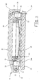
- FIG. 1 shows a connector assembly, designated generally by the reference numeral 10, mounted on a printed circuit board 12 and in which a contact according to this invention may be utilized.
- the connector assembly 10 is of the type utilized for burning or testing of an integrated circuit chip or a multi-chip subassembly and includes, generally, a body portion 14, a hinged cover member 16, and a latch member 18 for releasably securing the cover member 16 to the body portion 14 in a closed position.
- the body portion 14 is formed with a plurality of cavities 20, each for holding a single electrical contact, schematically shown at 22.
- the cavities 20 are arranged around the periphery of a central pocket 24, sized to accept the integrated circuit chip package 26.
- Within the bottom of the pocket 24 there is disposed a spring member 28 which is utilized to spring load the package 26 so that upon opening of the cover member 16, the package 26 is partially ejected.
- the package 26 is formed with terminals, leads, or pads along its periphery, illustratively depicted at 30. These terminals 30 are adapted for contact with respective ones of the contacts 22 disposed in the cavities 20. As schematically shown in Figure 1, each of the contacts 22 has a base portion 32 from which a downwardly depending contact leg, or terminal 34 extends for insertion into an appropriately sized and spaced opening through the printed circuit board 12, as is conventional in the art. Alternatively, the terminal 34 may be configured for surface mounting, in a conventional manner, as shown in Figure 1 at 34A.
- a contact arm 36 extends upwardly from the base portion 32 for surface contact with the package terminal 30 upon insertion of the package 26 into the pocket 24.
- the contact arm 36 exerts a contact force against the package terminal 30. If all elements could be made perfectly, and there were no variations in the size of the package 26, then this contact force could be generated by the inherent resiliency of the contact arm 36 cantilevered on the base portion 32. However, in the real world, there are manufacturing tolerances for the package 26 which vary from manufacturer to manufacturer. The contact arm 36 must be capable of accommodating these tolerances, which may be on the order of 0.030 inch (about 0.8mm) from the largest to the smallest size package, while still exerting an appropriate contact force.
- the contact arm 36 was constructed as a simple beam as shown in Figure 1, the large deflection from the largest size package 26 would deform the contact arm 36 beyond its elastic limits so that when a smaller package 26 was inserted in the pocket 24, the contact arm 36 could not spring back to apply the required contact force. If size were not at a premium, then the contact arm 36 could be lengthened. However, as previously described, size is limited. Thus, a contact 22 must be designed which is small in size and capable of accommodating the relatively large deflection noted above while still retaining its effective resiliency so that an appropriate contact force is generated over the entire range of package sizes.
- Figure 2 illustrates a kinematic model of a contact which transforms a large deflection of a short beam to a very small deflection at another location where a spring is acting, permitting the spring to stay within its elastic limit.
- the model includes a base 38 and a first beam 40 having a first end 42 and a second end 44. The first end 42 of the first beam 40 is attached to the base 38 for pivoting movement.
- a second beam 46 has a first end 48 pivotally attached to the first beam second end 44 at the pivot 49 and extends outwardly.
- the second beam second end 50 has pivotally attached thereto a first end 52 of a third beam 54 having a second end 58 pivotally attached to the base 38 at the pivot 59 as shown.
- a spring 56 resiliently couples the first beam second end 44 to the third beam second end 58. If a force is applied to the beam 40, as indicated by the arrow 64, this force being equivalent to the force exerted on the contact arm 36 by the package terminal 30 ( Figure 1), the beam 40 will be pivoted clockwise about its first end 42 to the position shown by the broken lines 60. This will cause the pivot point 59 at the third beam second end 58 to also pivot clockwise so that the distance between the pivot points 49 and 59 of the ends 44 and 58 respectively becomes slightly smaller by a fraction of the horizontal displacement of the first beam second end 44. Movement from the equilibrium position shown by the solid lines in Figure 2 to the position shown by the broken lines will be resisted by the spring 56.
- the spring 56 resiliently couples the area 65, where the force 64 is applied, to the base 38 so as to generate the desired contact force.
- the mechanism shown in Figure 2 will return from the displaced position shown by the broken lines 60 to the equilibrium position shown by the solid lines.
- the size of the cavity 20 is limited.
- the cavity may be 0.150 inch by 0.220 inch (about 3.8 mm by 5.6 mm) and must accommodate a contact having a thickness of 0.010 inch (about 0.25 mm).
- a mechanism of the complexity shown in Figure 2 cannot, at this time, be constructed with any practical technology to satisfy those size constraints.
- there can be constructed from a monolithic piece of metal a direct analog of the mechanism shown in Figure 2.
- the contact 66 is formed as a monolithic element from a planar metal sheet. It provides an electrical path between a first contact portion 68 and a second contact portion 70 as well as a contact force at the first contact portion 68, directed toward the left as viewed in Figure 3.
- the contact element 66 includes a base portion 72, from which the second contact portion 70 extends.
- a cantilevered member 74 has a first end 76 and a second end 78, the first end extending from the base portion 72 in a cantilevered fashion.
- the first contact portion 68 is formed as part of the member 74 adjacent the second end 78.
- a first pivotal zone 79 is provided in the area where the end 76 extends from the base 72.
- a generally C-shaped or other suitably shaped spring member 80 has a first end 82 pivotally associated, by means of a second pivotal zone 84 with the second end 78 of the cantilevered member 74, and a second end 88 pivotally associated, by means of a third pivotal zone 90 with the base 72.
- the contact 80 is formed by blanking out of a piece of flat sheet stock wherein the first contact portion 68 is in the position indicated by broken lines at B of Figure 3. A force is applied to the C-shaped spring member 80 to skew it to the left relative to the base 72 to create an overstress condition in the member 80 so that it takes a set.
- the first contact portion 68 With the force removed and the member 80 in equilibrium, the first contact portion 68 will now be in the position indicated by solid lines at A in Figure 3. Note that the skewing of the C-shaped spring member 80 to the left causes the member 74 to be preloaded, within its elastic limit, to the left. This effectively increases the operating range of deflection of the member 74 from the preloaded position A through the unloaded position B to a position C where the member 74 is at its maximum deflection to the right, as viewed in Figure 3, without taking a set. An overstress stop 94 projecting upwardly from the base 72 limits movement of the contact 66.
- a preferred embodiment of the contact 66 is shown in Figure 4 and indicated as 100. Similar elements of the two contacts 66 and 100 are indicated by similar designator numerals and will not be described again here.
- the contact 100 is substantially identical with the contact 66 in all respects except for the pivotal zone 90.
- the contact 100 includes a pivotal zone 102 which instead of utilizing plastic deformation of the metal to permit pivotal movement of the end 88, a two piece pivotal nesting structure is used.
- the portion 104 of this nesting structure which is attached to the end 88, is a free end which pivotally engages a nest 106 disposed in the base 72.
- This first embodiment of the contact is shown in Figure 4A as it would appear after blanking from sheet stock.
- the portion 104 is then urged to the left, as indicated by the arrow D in Figure 4A, into contact with a backing member 108 and into latching engagement with the nest 106.
- This movement to the left of the portion 104 causes the C-shaped member 80 to preload the cantilevered member 74 by moving the first contact portion 68 to the left to the position A, similar to the preloading of the member 74 of the contact 66.
- the backing member 108 serves to aid in the latching of the portion 104 to the nest 106.
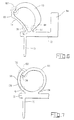
- a second embodiment of the inventive contact, indicated as 120, is shown in Figures 5 and 5A.
- a substantially circular spring member 122 has a first end 124 extending from a base 126 and a second end 128 which will be severed from the base along the broken lines 130 as a second manufacturing operation as explained below.
- a first contact portion 68 is disposed on the left most edge of the member 122 similar to the first contact portion 68 of the contacts 66 and 100.
- a tab 132 projects upwardly from the base 126 toward the interior of the circular spring member 122.
- the contact 120 is blanked from sheet stock in a manner similar to that of the contact 66 and will appear substantially as shown in Figure 5.
- the end 128 is severed from the base 126 along the broken lines 130 to form a latch keeper 134.
- the keeper 134 is forced out of the plane of the base 126, moved to the left and upwardly, and brought back into the plane of the base and latched onto the tab 132, as shown in Figure 5A.
- the portion 136 behaves similar to the cantilevered member 74 of the contact 100 by undergoing pivotal motion through a pivotal zone 79. Additionally, the portion 138 of the circular spring member 122 undergoes pivotal motion within the pivotal zone 84 in a manner similar to that of the contact 100.
- the contact 120 while of a slightly different shape, includes the functional elements of the contact 100 including: the cantilevered member 74,136; the first and second contact portions 68 and 70; a C-shaped spring member 80, (a portion of 122); the pivotal zones 79,84 and 102; and the base 72.
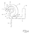
- FIG. 8 Another variation of the contact 100 is shown in Figure 8 and identified as 150.
- the contact 150 is similar to the contact 100 except that the cantilevered member 74 is replaced with a cantilevered serpentine-shaped member 152.
- the member 152 extends from the base 72 from the end 76, through the pivotal zone 79, through the serpentine shape to the end 78, which is pivotally associated by means of the pivotal zone 84 with the end 82 of the C-shaped spring member 80.
- the serpentine-shaped member 152 is arranged to resiliently respond to the usual contact engagement force, which would be in the direction of the arrow F as shown in Figure 8, by urging the first contact portion 68 a slight amount in the direction of the arrow W.
- the resiliency inherent in the serpentine-shaped member 152 will cause the first contacting portion 68 to wipe the mating surface a slight amount. This wiping action will clean the contacting surface of contaminants and result in a superior electrical connection.
- a very important aspect of the present invention is that a relatively large movement of the first contact portion 68 from its free form position represented by A in the figures, to a deflected position such as represented by B in the figures, results in a relatively small decrease in the distance between the two pivotal zones 84 and 102 (or 90). This is characteristic of all of the contacts 66,100,120,150, and the variations shown in Figure 6 and 7. This decrease in the distance between the two pivotal zones 84 and 102 is resisted by the C-shaped spring member 80,122 which provides the contact pressure urging the first contact portion 68 into pressing engagement with the mating surface 30. Since the C-shaped spring member 80,122 need move only a small amount in response to a relatively large movement of the first contact portion 68, the spring member 80,122 may be a very high compliance structure which will remain within its elastic limit when deflected.
Landscapes
- Engineering & Computer Science (AREA)
- Microelectronics & Electronic Packaging (AREA)
- Connecting Device With Holders (AREA)
- Coupling Device And Connection With Printed Circuit (AREA)
Applications Claiming Priority (2)
| Application Number | Priority Date | Filing Date | Title |
|---|---|---|---|
| US414561 | 1989-09-29 | ||
| US07/414,561 US4995816A (en) | 1989-09-29 | 1989-09-29 | Pivotal electrical contact |
Publications (2)
| Publication Number | Publication Date |
|---|---|
| EP0420008A2 true EP0420008A2 (de) | 1991-04-03 |
| EP0420008A3 EP0420008A3 (en) | 1992-01-08 |
Family
ID=23641984
Family Applications (1)
| Application Number | Title | Priority Date | Filing Date |
|---|---|---|---|
| EP19900117944 Withdrawn EP0420008A3 (en) | 1989-09-29 | 1990-09-18 | Pivotal electrical contact |
Country Status (4)
| Country | Link |
|---|---|
| US (1) | US4995816A (de) |
| EP (1) | EP0420008A3 (de) |
| KR (1) | KR950006026B1 (de) |
| CA (1) | CA2024035A1 (de) |
Cited By (2)
| Publication number | Priority date | Publication date | Assignee | Title |
|---|---|---|---|---|
| EP1475861A1 (de) * | 2003-05-06 | 2004-11-10 | Nihon Denshizairyo Kabushiki Kaisha | Elektrische Verbindungseinrichtung zwischen den Substraten |
| CN102742087A (zh) * | 2010-11-04 | 2012-10-17 | 欧姆龙株式会社 | 端子及使用其的连接器 |
Families Citing this family (15)
| Publication number | Priority date | Publication date | Assignee | Title |
|---|---|---|---|---|
| JPH07109780B2 (ja) * | 1991-02-19 | 1995-11-22 | 山一電機株式会社 | 電気部品用ソケットにおけるコンタクト |
| US5336096A (en) * | 1991-03-22 | 1994-08-09 | Enplas Corporation | IC socket and its contact pin |
| JP3016164B2 (ja) * | 1991-06-19 | 2000-03-06 | 日本エー・エム・ピー株式会社 | 可動型コネクタ |
| US5599194A (en) * | 1992-08-18 | 1997-02-04 | Enplas Corporation | IC socket and its contact pin |
| US5556306A (en) * | 1994-12-02 | 1996-09-17 | Hon Hai Precision Ind. Co., Ltd. | Stamped cantilever contact having closed-type engagement portion |
| US5771139A (en) * | 1995-08-03 | 1998-06-23 | Phase Metrics | Integrated spring head/gimbal assembly holder |
| US5874323A (en) * | 1997-08-28 | 1999-02-23 | Mcms, Inc. | Method of providing electrical contact to component leads |
| US5910024A (en) * | 1997-08-28 | 1999-06-08 | Mcms, Inc. | Carrier socket for receiving a damaged IC |
| US6794890B1 (en) * | 1999-07-27 | 2004-09-21 | Mitsubishi Denki Kabushiki Kaisha | Test socket, method of manufacturing the test socket, test method using the test socket, and member to be tested |
| JP2005129274A (ja) * | 2003-10-21 | 2005-05-19 | Fujitsu Ten Ltd | プレスフィット端子および接続構造 |
| JP2008196914A (ja) * | 2007-02-09 | 2008-08-28 | Micronics Japan Co Ltd | プローブおよびプローブ組立体 |
| DE102008007310B4 (de) * | 2008-02-02 | 2016-01-07 | Vincotech Holdings S.à.r.l. | Elektrischer Einpresskontakt |
| US8784145B2 (en) * | 2011-03-14 | 2014-07-22 | Omron Corporation | Terminal and connector using the same |
| CN103814479B (zh) * | 2011-09-14 | 2016-06-08 | 怡得乐工业有限公司 | 受约束的大挠曲绝缘位移端子和连接器 |
| JP5637336B2 (ja) * | 2012-03-15 | 2014-12-10 | オムロン株式会社 | 接続端子およびこれを用いたコネクタ |
Family Cites Families (8)
| Publication number | Priority date | Publication date | Assignee | Title |
|---|---|---|---|---|
| US4370017A (en) * | 1980-11-20 | 1983-01-25 | Amp Incorporated | Complanate contact terminal |
| US4354729A (en) * | 1980-12-22 | 1982-10-19 | Amp Incorporated | Preloaded electrical contact terminal |
| US4513353A (en) * | 1982-12-27 | 1985-04-23 | Amp Incorporated | Connection of leadless integrated circuit package to a circuit board |
| US4504887A (en) * | 1983-04-01 | 1985-03-12 | Amp Incorporated | Leadless integrated circuit package housing having means for contact replacement |
| US4684184A (en) * | 1986-01-14 | 1987-08-04 | Amp Incorporated | Chip carrier and carrier socket for closely spaced contacts |
| US4832617A (en) * | 1988-03-31 | 1989-05-23 | Foxx Conn International, Inc. | Circuit board socket, contact and method of manufacture |
| US4927369A (en) * | 1989-02-22 | 1990-05-22 | Amp Incorporated | Electrical connector for high density usage |
| US4906194A (en) * | 1989-04-13 | 1990-03-06 | Amp Incorporated | High density connector for an IC chip carrier |
-
1989
- 1989-09-29 US US07/414,561 patent/US4995816A/en not_active Expired - Fee Related
-
1990
- 1990-08-27 CA CA002024035A patent/CA2024035A1/en not_active Abandoned
- 1990-09-18 EP EP19900117944 patent/EP0420008A3/en not_active Withdrawn
- 1990-09-26 KR KR1019900015246A patent/KR950006026B1/ko not_active Expired - Fee Related
Cited By (3)
| Publication number | Priority date | Publication date | Assignee | Title |
|---|---|---|---|---|
| EP1475861A1 (de) * | 2003-05-06 | 2004-11-10 | Nihon Denshizairyo Kabushiki Kaisha | Elektrische Verbindungseinrichtung zwischen den Substraten |
| CN102742087A (zh) * | 2010-11-04 | 2012-10-17 | 欧姆龙株式会社 | 端子及使用其的连接器 |
| CN102742087B (zh) * | 2010-11-04 | 2015-04-08 | 欧姆龙株式会社 | 端子及使用其的连接器 |
Also Published As
| Publication number | Publication date |
|---|---|
| US4995816A (en) | 1991-02-26 |
| EP0420008A3 (en) | 1992-01-08 |
| KR910007187A (ko) | 1991-04-30 |
| KR950006026B1 (ko) | 1995-06-07 |
| CA2024035A1 (en) | 1991-03-30 |
Similar Documents
| Publication | Publication Date | Title |
|---|---|---|
| US4995816A (en) | Pivotal electrical contact | |
| US4330163A (en) | Zero insertion force connector for LSI circuit package | |
| USRE33268E (en) | Chip carrier socket having improved contact terminals | |
| US4547031A (en) | Chip carrier socket and contact | |
| US6149468A (en) | Card edge connector | |
| EP0632542B1 (de) | Leiterplattenrandverbinder mit Verriegelungsvorrichtung | |
| JP2000506638A (ja) | スマートカード及びスマートカード用コネクタ | |
| JP3403098B2 (ja) | Icカード用コネクタ | |
| JPH11512229A (ja) | 減少した自己インダクタンスを有する電気コンタクト | |
| US5904580A (en) | Elastomeric connector having a plurality of fine pitched contacts, a method for connecting components using the same and a method for manufacturing such a connector | |
| KR20020045557A (ko) | 이방향 변위를 나타내는 스위치 | |
| EP0407531B1 (de) | Chipträger-sockel niedriger bauhöhe | |
| US4959029A (en) | Electrical contact | |
| EP1349240B1 (de) | Verbinder mit Kontaktteil dessen Bewegung vom Isolator geführt wird | |
| US4995817A (en) | Electrical contact | |
| US6899565B2 (en) | Electrical connector having a holddown for ground connection | |
| US5916000A (en) | Press fit electrical contact | |
| EP1626461B1 (de) | IC-Fassung | |
| JP5451244B2 (ja) | Icカード用コネクタ | |
| US20030162417A1 (en) | Connector suitable for connecting a pair of circuit boards arranged in parallel | |
| US4968259A (en) | High density chip carrier socket | |
| US6231395B1 (en) | Card reader connector, with elastic brush contacts, and reader comprising same | |
| KR100394337B1 (ko) | 전기부품용 소켓 | |
| JP2709975B2 (ja) | 電気コンタクト | |
| US20050095906A1 (en) | Socket connector with reliable retaining means |
Legal Events
| Date | Code | Title | Description |
|---|---|---|---|
| PUAI | Public reference made under article 153(3) epc to a published international application that has entered the european phase |
Free format text: ORIGINAL CODE: 0009012 |
|
| 17P | Request for examination filed |
Effective date: 19901220 |
|
| AK | Designated contracting states |
Kind code of ref document: A2 Designated state(s): DE FR GB IT NL |
|
| PUAL | Search report despatched |
Free format text: ORIGINAL CODE: 0009013 |
|
| AK | Designated contracting states |
Kind code of ref document: A3 Designated state(s): DE FR GB IT NL |
|
| RAP1 | Party data changed (applicant data changed or rights of an application transferred) |
Owner name: THE WHITAKER CORPORATION |
|
| 17Q | First examination report despatched |
Effective date: 19940328 |
|
| STAA | Information on the status of an ep patent application or granted ep patent |
Free format text: STATUS: THE APPLICATION IS DEEMED TO BE WITHDRAWN |
|
| 18D | Application deemed to be withdrawn |
Effective date: 19940809 |