EP0412887A1 - Mit hohem Wirkungsgrad kathodolumineszenter Schirm für hochleuchtende KathodenstrahlrÀ¶hre - Google Patents
Mit hohem Wirkungsgrad kathodolumineszenter Schirm für hochleuchtende KathodenstrahlrÀ¶hre Download PDFInfo
- Publication number
- EP0412887A1 EP0412887A1 EP90402235A EP90402235A EP0412887A1 EP 0412887 A1 EP0412887 A1 EP 0412887A1 EP 90402235 A EP90402235 A EP 90402235A EP 90402235 A EP90402235 A EP 90402235A EP 0412887 A1 EP0412887 A1 EP 0412887A1
- Authority
- EP
- European Patent Office
- Prior art keywords
- substrate
- layer
- intermediate layer
- refractive index
- cathodoluminescent screen
- Prior art date
- Legal status (The legal status is an assumption and is not a legal conclusion. Google has not performed a legal analysis and makes no representation as to the accuracy of the status listed.)
- Granted
Links
Images


Classifications
-
- H—ELECTRICITY
- H01—ELECTRIC ELEMENTS
- H01J—ELECTRIC DISCHARGE TUBES OR DISCHARGE LAMPS
- H01J29/00—Details of cathode-ray tubes or of electron-beam tubes of the types covered by group H01J31/00
- H01J29/02—Electrodes; Screens; Mounting, supporting, spacing or insulating thereof
- H01J29/10—Screens on or from which an image or pattern is formed, picked up, converted or stored
- H01J29/18—Luminescent screens
- H01J29/185—Luminescent screens measures against halo-phenomena
-
- H—ELECTRICITY
- H01—ELECTRIC ELEMENTS
- H01J—ELECTRIC DISCHARGE TUBES OR DISCHARGE LAMPS
- H01J2229/00—Details of cathode ray tubes or electron beam tubes
- H01J2229/89—Optical components associated with the vessel
- H01J2229/8913—Anti-reflection, anti-glare, viewing angle and contrast improving treatments or devices
- H01J2229/8916—Anti-reflection, anti-glare, viewing angle and contrast improving treatments or devices inside the vessel
Definitions
- the invention relates to a cathodoluminescent screen for cathode ray tubes and particularly for high luminance tubes, such as for example tubes of the so-called "projection" type.
- the object of the invention is to show a cathodoluminescent screen arranged in a new way which makes it possible, in particular to better concentrate the light emitted by this screen on axes perpendicular to the latter, that is to say which makes it possible to obtain , from each elementary image point on the screen, a more concentrated emission indicator on the axis.
- One of the main aims, in the context of the so-called "projection" type of tube technique, is thus to improve the efficiency of capture, by projection optics, of the light emitted by the tube.
- the cathodoluminescent screen generally comprises a glass slab serving as a substrate, on which is produced at least one luminescent layer which, most often, consists of grains of phosphors.
- the cathode ray tube contains an electron source which makes it possible to produce a beam, which beam is accelerated and focused before bombarding the layer of phosphors. Under the effect of this bombardment, the phosphors emit light, and a bright image can be formed on the surface of the screen by deflecting the beam.
- the resolution of the image depends in particular on the focusing of the beam, but it also depends on the characteristics of the cathodoluminescent screen, this screen having also effects on light output and luminance in general.
- FIG. 1 shows partially and schematically in a sectional view, a conventional cathodoluminescent screen for cathode ray tubes.
- This screen 1 comprises a glass slab 2 forming a substrate.
- the substrate 2 carries a luminescent layer 3 formed for example from a plurality of phosphor grains L1, L2, ..., Ln.
- the glass substrate 2 In a cathode ray tube, the glass substrate 2 generally has a thickness E of the order of 6 to 7 millimeters, and its refractive index n0 is of the order of 1.5. Under these conditions, the light emitted under the impact of an electron beam (symbolized by an arrow 13) by the layer 3 of phosphors, by a grain L1 for example which is in contact with an inner face 5 of the substrate 2 , can exit through a face 6 of the latter towards the outside of the tube, only for its part whose angle of incidence (in the substrate 2) is less than the limit angles ⁇ 0, ⁇ 0 ′ formed between rays R1, R1 ′ (Which represent the limit refraction) and an axis x normal to the plane of the external face 6 of the substrate 2.
- this light undergoes a total reflection (as illustrated by the radius R1) by which it is returned towards the internal face 5 of the substrate 2, where it is again reflected towards opposite side 6, unless it meets a luminous grain ophore in touch with this inner face 5; in the latter case, this light can be re-emitted towards use as symbolized by arrows RD1, RD2, RD3.
- This phenomenon which can be repeated several times, is at the base of the creation of a large halo which tends to degrade significantly the contrast of images, and in another way, the light energy of the peak central, that is to say the light energy emitted along the axis normal to the plane of the substrate 2.
- FIG. 2 illustrates this situation and shows for this purpose the front of a conventional cathode ray tube T comprising a cathodoluminescent screen, such as for example the screen 1 of FIG. 1, and schematically shows the lens 7 of the optics of a conventional projection device also.
- a light is produced, part of which is emitted with an angle of incidence equal to or greater than the limit angle ⁇ 0, as illustrated by the limit radius R1.
- This light can undergo multiple reflections or be redistributed towards use according to rays RD1, RD2, R3, so that this light which is represented by the limit radius R1 generates the halo.
- the use consists of the lens 7 which represents the optical means of a projection system.
- the lens 7 has an opening 8 centered on an axis 9 of the tube T, the axis 9 being normal to the plane of the screen 1.
- the light emitted with an angle of incidence less than the limit angle ⁇ 0 leaves the tube T, that is to say the substrate 2.
- This light is captured by the use only for its part which passes through the aperture 8 of the lens 7, as illustrated by a useful radius RU which is emitted from point A.
- the other part of this light is symbolized by a ray RP leaving the tube T but which does not pass not through opening 8, and which is therefore lost for use, which degrades the light output.
- the rays re-broadcast towards the use and picked up by the latter can have a harmful effect, such as for example the re-broadcast ray RD2 which, although parallel to the axis 9, is re-broadcast from a point different from point A and tends to destroy the contrast.
- the invention constitutes a solution to the problems set out above, a particularly advantageous solution in particular because the invention is simple to implement and, as a result, it constitutes an inexpensive solution making it possible in particular to obtain a maximum gain of luminance, to improve the contrast and to strongly decrease the halo.
- a cathodoluminescent screen for cathode ray tubes comprising a substrate having a given thickness and a given refractive index, the substrate carrying a luminescent layer subjected to electronic bombardment and producing a light under the effect of said bombardment, characterized in that an intermediate layer is disposed between the luminescent layer and the substrate, the intermediate layer having on the one hand a second thickness much less than the thickness of the substrate, and on the other hand having a second refractive index higher than the refractive index of the substrate.
- a refractive surface is created at the faces in contact with the intermediate layer and the substrate, a refractive surface which totally reflects the light coming from the luminescent layer when this light arrives with an angle of incidence more large than a limiting angle ⁇ l1 whose value is deduced from that of the refractive indices of the substrate and the middle layer.
- the limit angle ⁇ l1 is less than another limit angle ⁇ 0 which causes total reflection of the light at the interface between the substrate and the air under conditions similar to those which have already been mentioned in the preamble to explain the faults of the prior art, and which lead to causing a large halo.
- the interposition of the intermediate layer has the effect of diffusing a very large part of the light, beyond the limiting angle of refraction ⁇ l1, towards the cathodoluminescent layer, so that this light is retransmitted or redistributed towards the outside of the tube, that is to say towards use, with an emission indicator much more concentrated on the axis.
- the light redistribution efficiency can be greatly promoted by the implantation of a compact monolayer of fine grains, between the intermediate layer and the luminescent layer or phosphor layer.
- FIG. 3 partially shows a cathodoluminescent screen 10 according to the invention, intended to form the screen of a cathode ray tube.
- the screen 10 comprises a substrate 11, constituted for example in a conventional manner by a glass slab having a thickness E1 of the order of 6 to 7 millimeters.
- the substrate 11 carries a luminescent layer 12 exposed to an electron beam symbolized by an arrow 13.
- the luminescent layer 12 is traditionally constituted by a plurality of phosphor grains L1, L2, ..., Ln.
- a conductive layer 4, made of aluminum for example, is deposited on the luminescent layer 12, in particular for reflecting the light produced by the luminescent layer 12 towards use, that is to say towards an outer face 14 of the substrate 11, face outside which it is in contact with air.
- an intermediate layer 15 is interposed between the luminescent layer 12 and the substrate 11.
- the intermediate layer 15 is made for example of a dielectric material, transparent to the light emitted by the phosphors L1 to Ln and having a refractive index n1 greater than the refractive index n0 (n0 substantially equal to 1.5) of the substrate 11, and preferably much greater than this refractive index n0 of the substrate (for example n0 / n1 equal to or less than 0.75).
- the intermediate layer 15 can be made of titanium oxide TiO2 or also of zinc sulfide ZnS, so as to have a refractive index n1 of the order of 2.35.
- the intermediate layer 15 has a thickness E2 much less than the thickness E1 of the substrate 11.
- the intermediate layer 15 constitutes a thin layer which can be carried out in a simple and inexpensive manner by evaporation, or even for example by a dip alcoholate method from a titanium alcoholate T i (OC2H5) 4.
- the thickness E2 of the intermediate layer 15 is not really critical for operation, the important thing being that it is much smaller than the thickness E1 of the substrate 11; very satisfactory results have been obtained with values close to the micrometer for the thickness E2 of the intermediate layer 15. It note that in the figures the scale of dimensions is not respected.
- the trajectory of the first photon p1 is such that it has an angle ⁇ 1 less than the limit angle ⁇ l1, which allows it to cross the interface between the intermediate layer and the substrate 15-11, then leave the substrate 11 by the external face 14 of the latter if its trajectory forms, with an axis x normal to the external face 14, an angle ⁇ 1 ′ smaller than a limit angle ⁇ 0 given by the indices of the substrate 11 and of the 'air; the limiting angle ⁇ 0 in the substrate 11 having a value similar to that mentioned in the preamble, namely of the order of 43 ° (the outer face 14 represents a refractive surface formed at the interface of the substrate 11 and the air).
- this second photon p2 is reflected at a point marked c of this interface, towards the luminescent layer 12 and, if it encounters a grain of phosphor L1 to Ln in contact with an upper face 16 of the intermediate layer 15, at a point f for example, this photon p2 is rebroadcast in the direction of the substrate 11 into which it can penetrate or not depending on whether its angle of incidence is less than the limit angle ⁇ l1 or not.
- this photon can be redistributed towards the substrate 11, that is to say towards the outside as symbolized by arrows marked RD; but if there are no phosphors at point f, the second p2 is reflected towards the interface 15-11 with an angle greater than the limit angle ⁇ l1, so that this photon will be reflected again by the interface 15-11 towards the luminescent layer 12.
- this distance D2 is of the order of 2 micrometers.
- the configuration of the invention induces this redistribution much closer to the point where the light was emitted. Consequently we suppress the intensity of the halo at long distance, and by combining this with the fact that in the intermediate layer 15 the amount of light which undergoes a total reflection is increased, an emission indicator more concentrated on the axis is obtained than in the prior art, that is to say that the intensity of the light emitted along the axis normal to the plane of the substrate 11.
- FIG. 4 illustrates a preferred version of the invention, in which the efficiency of redistribution of the light which has been reflected by the interface intermediate layer-substrate 15-11 is improved.
- a diffusing layer 20 is arranged between the intermediate layer 15 and the luminescent layer 12 or layer of phosphors.
- the diffusing layer 20 is constituted by fine grains G1, G2, ..., GN which form a compact monolayer, and which make it possible to greatly improve the collection of light after total reflection by the interface 15-11.
- the finer and closer the grains G1 to GN the more the contact points are numerous for the recovery of light above the intermediate layer 15.
- fine grains we will define grains whose average diameter is less than the average diameter of phosphor grains L1 to Ln of the luminescent layer 12.
- the grains G1 to GN can have an average diameter of the order of for example 1 micrometer, and according to another characteristic of the invention, they can be advantageously formed, themselves by phosphors of the same nature as the phosphors of the luminescent layer 12, so as to also participate in the light production.
- monolayer we mean a layer whose thickness includes a single grain, this for the entire surface of the layer (although in practice there may remain locally some exceptions to this rule without degrading the resolution).
- the screen 10 of the invention may further comprise a bonding layer 22 which is both in contact with the face upper 16 of the intermediate layer 15, and in contact with the grains G1 to GN of the diffusing monolayer 20.
- the bonding layer 22 makes it possible to improve the collection of light by preventing, by its presence, that the light rays do not undergo a reflection total at the level of the upper face 16 of the intermediate layer 15, when these light rays reach this upper face 16 at a point located between two grains G1 with neighboring GN, as illustrated in FIG. 3 by way of example by a third photon p3.
- the bonding layer 22 has a refractive index n2 greater than or equal to the refractive index n1 of the intermediate layer 15.
- the bonding layer 22 can constitute a dielectric layer produced for example by titanium oxide TiO2 by the same method as the intermediate layer 15.
- the photon p3 can be emitted in the intermediate layer 15 by a grain G2 for example of the diffusing layer 20.
- the photon p3 undergoes reflection at the level of the intermediate layer-substrate interface 15-11, reflection which returns it to the upper face 16.
- the photon p3 In the absence of the bonding layer 22, the photon p3 would be reflected at a point O2 of this upper face 16, as it is represented by an arrow in dotted lines marked p3 ′, except of course if the point O2 is sufficiently close to a grain G1 at GN so that the phenomenon of evanescent waves can manifest itself, and allows the photon p3 to exit from the intermediate layer 15 and penetrate into the grain. With the presence of the bonding layer 22, the photon p3, even if it arrives at the upper face 16 at a point of the latter relatively distant from a grain, this photon p3 leaves the intermediate layer 15, and the layer link 22 picks up this photon and channels it to a third grain G3, for example where it is diffused to the outside.
- the bonding layer 22 also makes it possible to provide a particularly advantageous thermal junction function in the application to projection, a function which is also useful if the grains G1 to GN of the diffusing monolayer 20 are grains of phosphors.
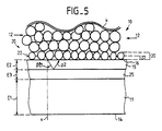
- FIG. 5 shows another version of the invention which makes it possible to reinforce the effect obtained by the interposition of the intermediate layer 15.
- a second intermediate layer 25 is disposed between the substrate 11 and the first intermediate layer 15.
- this second intermediate layer 25 has a refractive index n3 lower than the refractive index n0 of the substrate 11.
- this second intermediate layer 25 has a thickness E3 of the same order of magnitude that the thickness E2 of the first intermediate layer 15, that is to say close to 1 micrometer; but it should be noted that this thickness E3 is not critical, the important thing being that it is very small compared to the thickness E1 of the substrate 11.
- the second intermediate layer 25 can be produced for example from magnesium fluoride MgF2 of which the refractive index n3 is of the order of 1.35, by a conventional method of evaporation.
- This new configuration makes it possible to reduce the value of the limit angle ⁇ l1 in the first intermediate layer 15.
- the limit angle ⁇ 1 beyond which the photon p2 is reflected towards the upper face 16 of the first intermediate layer 15 this angle limits to a lower value in the case of this new version of the invention than in the case represented in FIG. 3.
- the new value of the limit angle ⁇ l1 is of the order of 35 °, This is due to the fact that the difference in refractive index between the index n1 of the first layer intermediate 15 and the index n3 of the second intermediate layer 25 is greater than the difference in index between the intermediate layer 15 and the substrate 11 shown in FIG. 3. As mentioned above, this reinforces the effects produced by the intermediate layer 15, and makes it possible to increase the light emission indicator as much as possible and thus obtain the maximum luminance gain by a concentration of the angle (not shown) of the light indicator.
- the second intermediate layer 25 can be an even lower refractive index n3, if this second intermediate layer 25 consists of a microporous layer.
- the second intermediate layer 25 can be a microporous layer of silicon oxide SiO2, the refractive index of which can be close to 1.25, which makes it possible to obtain an even smaller limit angle ⁇ l1 of the order of 32 °.
- This second intermediate layer formed of a porous layer of silicon oxide can be deposited on the substrate 11 in a conventional manner in itself, for example by an ultracentrifugation method whose implementation is easy, or also by a wet densification process which leads to a deposit, the degree of porosity of which depends on the conditions of use.
- the nature of the materials capable of forming the different layers namely the first intermediate layer 15, the second intermediate layer 25, the diffusing layer 20, the bonding layer 22, the nature of these materials is indicated as in no way limiting example, and other materials can be chosen in particular according to the color of the light.
- the use of such materials makes it possible to obtain luminance gains of the order of 40%, for green and blue in particular, and greater than 40% for red in the case of the use of Fe2O3.
Landscapes
- Cathode-Ray Tubes And Fluorescent Screens For Display (AREA)
Applications Claiming Priority (2)
| Application Number | Priority Date | Filing Date | Title |
|---|---|---|---|
| FR8910828A FR2650914A1 (fr) | 1989-08-11 | 1989-08-11 | Ecran cathodoluminescent a haute efficacite pour tubes a rayons cathodiques haute luminance |
| FR8910828 | 1989-08-11 |
Publications (2)
| Publication Number | Publication Date |
|---|---|
| EP0412887A1 true EP0412887A1 (de) | 1991-02-13 |
| EP0412887B1 EP0412887B1 (de) | 1994-07-06 |
Family
ID=9384667
Family Applications (1)
| Application Number | Title | Priority Date | Filing Date |
|---|---|---|---|
| EP90402235A Expired - Lifetime EP0412887B1 (de) | 1989-08-11 | 1990-08-03 | Mit hohem Wirkungsgrad kathodolumineszenter Schirm für hochleuchtende Kathodenstrahlröhre |
Country Status (5)
| Country | Link |
|---|---|
| US (1) | US5101136A (de) |
| EP (1) | EP0412887B1 (de) |
| JP (1) | JPH03129642A (de) |
| DE (1) | DE69010423T2 (de) |
| FR (1) | FR2650914A1 (de) |
Families Citing this family (5)
| Publication number | Priority date | Publication date | Assignee | Title |
|---|---|---|---|---|
| JPH08129963A (ja) * | 1994-10-31 | 1996-05-21 | Hitachi Ltd | カラー陰極線管 |
| DE69510170T2 (de) * | 1994-12-26 | 1999-11-04 | Toshiba Kawasaki Kk | Bildschirm und Verfahren zur Herstellung desselben |
| KR100315007B1 (ko) * | 1995-11-22 | 2002-02-28 | 이시다 아키라 | 카세트내의 기판 검출 및 반송장치와 그 방법 |
| US6812636B2 (en) * | 2001-03-30 | 2004-11-02 | Candescent Technologies Corporation | Light-emitting device having light-emissive particles partially coated with light-reflective or/and getter material |
| JP2006228498A (ja) * | 2005-02-16 | 2006-08-31 | Sonac Kk | 表示装置用蛍光面およびこれを備えた表示装置 |
Citations (2)
| Publication number | Priority date | Publication date | Assignee | Title |
|---|---|---|---|---|
| EP0018666A1 (de) * | 1979-05-07 | 1980-11-12 | Optical Coating Laboratory, Inc. | Bildschirmaufbau für Kathodenstrahlröhren zur Unterdrückung der Lichthofbildung und Verfahren |
| EP0018667A1 (de) * | 1979-05-07 | 1980-11-12 | Optical Coating Laboratory, Inc. | Bildschirmaufbau für Kathodenstrahlröhren mit reduzierter Reflexion zur Unterdrückung der Lichthofbildung |
Family Cites Families (4)
| Publication number | Priority date | Publication date | Assignee | Title |
|---|---|---|---|---|
| JPS577048A (en) * | 1980-06-16 | 1982-01-14 | Toshiba Corp | Fluorescent light emission screen |
| JPS6012650A (ja) * | 1983-07-01 | 1985-01-23 | Mitsubishi Electric Corp | 陰極線管 |
| NL8402304A (nl) * | 1984-07-20 | 1986-02-17 | Philips Nv | Beeldbuis. |
| US4633131A (en) * | 1984-12-12 | 1986-12-30 | North American Philips Corporation | Halo-reducing faceplate arrangement |
-
1989
- 1989-08-11 FR FR8910828A patent/FR2650914A1/fr not_active Withdrawn
-
1990
- 1990-08-03 EP EP90402235A patent/EP0412887B1/de not_active Expired - Lifetime
- 1990-08-03 DE DE69010423T patent/DE69010423T2/de not_active Expired - Fee Related
- 1990-08-09 JP JP2211430A patent/JPH03129642A/ja active Pending
- 1990-08-10 US US07/565,680 patent/US5101136A/en not_active Expired - Lifetime
Patent Citations (2)
| Publication number | Priority date | Publication date | Assignee | Title |
|---|---|---|---|---|
| EP0018666A1 (de) * | 1979-05-07 | 1980-11-12 | Optical Coating Laboratory, Inc. | Bildschirmaufbau für Kathodenstrahlröhren zur Unterdrückung der Lichthofbildung und Verfahren |
| EP0018667A1 (de) * | 1979-05-07 | 1980-11-12 | Optical Coating Laboratory, Inc. | Bildschirmaufbau für Kathodenstrahlröhren mit reduzierter Reflexion zur Unterdrückung der Lichthofbildung |
Non-Patent Citations (1)
| Title |
|---|
| PATENT ABSTRACTS OF JAPAN vol. 6, no. 64 (E-103)(942) 23 avril 82, & JP-A-57 7048 (TOKYO SHIBAURA DENKI) 14 janvier 1982, * |
Also Published As
| Publication number | Publication date |
|---|---|
| US5101136A (en) | 1992-03-31 |
| EP0412887B1 (de) | 1994-07-06 |
| JPH03129642A (ja) | 1991-06-03 |
| DE69010423D1 (de) | 1994-08-11 |
| FR2650914A1 (fr) | 1991-02-15 |
| DE69010423T2 (de) | 1994-10-20 |
Similar Documents
| Publication | Publication Date | Title |
|---|---|---|
| EP0323317B1 (de) | Verfahren zur Herstellung von Mikro-Lichtleitern mit niedrigen optischen Ausbreitungsverlusten durch Aufbringen von Mehrfachschichten | |
| EP0186225B1 (de) | Bilddetektor für eine Kamera mit "Tag-Nacht"-Arbeitsweise | |
| EP0428667B1 (de) | Eingangsschirm für eine röntgenbildverstärkerröhre | |
| EP2583299B1 (de) | Faseroptischer phosphorschirm mit winkelfilter | |
| EP0412887B1 (de) | Mit hohem Wirkungsgrad kathodolumineszenter Schirm für hochleuchtende Kathodenstrahlröhre | |
| EP0319080B1 (de) | Röntgenstrahl-Bildverstärkerröhre | |
| JPH08250051A (ja) | マイクロチャネルプレート及び光電子増倍管 | |
| FR3071788A1 (fr) | Systeme d'observation de conducteur et son procede de saisie par le systeme et le procede de fabrication du systeme | |
| EP0553578B1 (de) | Bildverstärkerröhre mit Intensitätsverteilungkompensation | |
| EP0056671B1 (de) | Photoelektrische Detektorvorrichtung | |
| EP0125962B1 (de) | Röntgenbildverstärker und dessen Anwendung bei rechnergestützter Röntgenaufnahmetechnik | |
| FR2545269A1 (fr) | Ecran electroluminescent et son procede de fabrication | |
| EP0182405B1 (de) | Photoelektrische Vorrichtung zum Nachweisen leuchtender Ereignisse | |
| EP0143714B1 (de) | Lumineszenter Schirm und Verfahren zur Herstellung desselben | |
| FR2768522A1 (fr) | Detecteur a scintillation, revetement refracteur pour scintillateur et procede de fabrication d'un tel revetement | |
| EP0851455B1 (de) | Röntgenbildverstärkerröhre | |
| EP0079651B1 (de) | Photoelektrischer Detektor | |
| WO1990014680A1 (fr) | Ecran cathodoluminescent a film mince pour tube a rayons cathodiques a haute luminance | |
| FR2491677A1 (fr) | Multiplicateur d'electrons, procede de fabrication et tubes images comportant ledit multiplicateur | |
| JPH0249125A (ja) | ストリーク管 | |
| FR2647591A1 (fr) | Ecran cathodoluminescent a duree de vie elevee pour tubes a rayons cathodiques | |
| WO1992004737A1 (fr) | Detecteur infrarouge a substrat aminci et procede de fabrication | |
| FR2536616A1 (fr) | Dispositif analyseur d'images pour une camera de television en couleurs |
Legal Events
| Date | Code | Title | Description |
|---|---|---|---|
| PUAI | Public reference made under article 153(3) epc to a published international application that has entered the european phase |
Free format text: ORIGINAL CODE: 0009012 |
|
| AK | Designated contracting states |
Kind code of ref document: A1 Designated state(s): DE FR GB NL |
|
| 17P | Request for examination filed |
Effective date: 19910318 |
|
| 17Q | First examination report despatched |
Effective date: 19930119 |
|
| GRAA | (expected) grant |
Free format text: ORIGINAL CODE: 0009210 |
|
| AK | Designated contracting states |
Kind code of ref document: B1 Designated state(s): DE FR GB NL |
|
| REF | Corresponds to: |
Ref document number: 69010423 Country of ref document: DE Date of ref document: 19940811 |
|
| GBT | Gb: translation of ep patent filed (gb section 77(6)(a)/1977) |
Effective date: 19940819 |
|
| PLBE | No opposition filed within time limit |
Free format text: ORIGINAL CODE: 0009261 |
|
| STAA | Information on the status of an ep patent application or granted ep patent |
Free format text: STATUS: NO OPPOSITION FILED WITHIN TIME LIMIT |
|
| 26N | No opposition filed | ||
| REG | Reference to a national code |
Ref country code: GB Ref legal event code: IF02 |
|
| PGFP | Annual fee paid to national office [announced via postgrant information from national office to epo] |
Ref country code: NL Payment date: 20080803 Year of fee payment: 19 Ref country code: DE Payment date: 20080825 Year of fee payment: 19 |
|
| PGFP | Annual fee paid to national office [announced via postgrant information from national office to epo] |
Ref country code: GB Payment date: 20080718 Year of fee payment: 19 |
|
| PGFP | Annual fee paid to national office [announced via postgrant information from national office to epo] |
Ref country code: FR Payment date: 20090821 Year of fee payment: 20 |
|
| REG | Reference to a national code |
Ref country code: NL Ref legal event code: V1 Effective date: 20100301 |
|
| GBPC | Gb: european patent ceased through non-payment of renewal fee |
Effective date: 20090803 |
|
| PG25 | Lapsed in a contracting state [announced via postgrant information from national office to epo] |
Ref country code: NL Free format text: LAPSE BECAUSE OF NON-PAYMENT OF DUE FEES Effective date: 20100301 Ref country code: DE Free format text: LAPSE BECAUSE OF NON-PAYMENT OF DUE FEES Effective date: 20100302 |
|
| PG25 | Lapsed in a contracting state [announced via postgrant information from national office to epo] |
Ref country code: GB Free format text: LAPSE BECAUSE OF NON-PAYMENT OF DUE FEES Effective date: 20090803 |