EP0408124A2 - Schutzschaltung gegen negative Überspannungen über der Stromversorgung einer integrierten Schaltung mit einer Leistungseinrichtung und seinem Regelkreis - Google Patents
Schutzschaltung gegen negative Überspannungen über der Stromversorgung einer integrierten Schaltung mit einer Leistungseinrichtung und seinem Regelkreis Download PDFInfo
- Publication number
- EP0408124A2 EP0408124A2 EP90201804A EP90201804A EP0408124A2 EP 0408124 A2 EP0408124 A2 EP 0408124A2 EP 90201804 A EP90201804 A EP 90201804A EP 90201804 A EP90201804 A EP 90201804A EP 0408124 A2 EP0408124 A2 EP 0408124A2
- Authority
- EP
- European Patent Office
- Prior art keywords
- transistor
- circuit
- power device
- power supply
- voltage
- Prior art date
- Legal status (The legal status is an assumption and is not a legal conclusion. Google has not performed a legal analysis and makes no representation as to the accuracy of the status listed.)
- Granted
Links
Images


Classifications
-
- H—ELECTRICITY
- H02—GENERATION; CONVERSION OR DISTRIBUTION OF ELECTRIC POWER
- H02H—EMERGENCY PROTECTIVE CIRCUIT ARRANGEMENTS
- H02H9/00—Emergency protective circuit arrangements for limiting excess current or voltage without disconnection
- H02H9/04—Emergency protective circuit arrangements for limiting excess current or voltage without disconnection responsive to excess voltage
- H02H9/045—Emergency protective circuit arrangements for limiting excess current or voltage without disconnection responsive to excess voltage adapted to a particular application and not provided for elsewhere
- H02H9/047—Free-wheeling circuits
-
- H—ELECTRICITY
- H02—GENERATION; CONVERSION OR DISTRIBUTION OF ELECTRIC POWER
- H02H—EMERGENCY PROTECTIVE CIRCUIT ARRANGEMENTS
- H02H9/00—Emergency protective circuit arrangements for limiting excess current or voltage without disconnection
- H02H9/04—Emergency protective circuit arrangements for limiting excess current or voltage without disconnection responsive to excess voltage
Definitions
- the present invention relates to a circuit for protection against negative overvoltages acorss the power supply of an integrated circuit comprising a power device with related control circuit.
- power devices are used for driving loads of various types. If it is an inductive load, as in the case of a power device used in motor car applications, the cut-offs of the power device determine positive overvoltages across the power device itself which are normally absorbed by means of appropriate limiting devices such as zener diodes. It can, however, occur that such positive overvoltages across the power device combine with negative overvoltages across the source of the power supply, say, a motor vehicle's battery. In such cases, if the power device and the related control circuit are accomplished in the form of an integrated circuit, the parasite transistor formed between the collector of the power device and the power supply source can burn out.
- the object of the present invention is to endow the integrated circuit with an adequate protection against the drawbacks due to such negative overvoltages.
- a protection circuit characterized in that it comprises a switch sensitive to negative overvoltages across the power supply and suitable for enabling a limiter of the voltage applied across the power device.
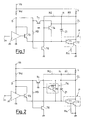
- a load L is driven by a power device P, which comprises two transistors T1 and T2, respectively, in a darlington configuration supplied with a voltage Vb and driven by a transistor T3, whose base is connected to the output of a control circuit constituted by a driver amplifier A1 suitable for receiving an input signal In.
- the collector of said transistor T3 is connected to a circuit node D, in turn connected to the power supply of amplifier A1 and, by means of a resistance Rd, to the power supply source Vb, while the emitter is connected to the base of transistor T1.
- a resistor R4 connects the base of transistor T2 to the emitter of the same transistor T2 and to ground.
- a voltage limiter comprising a transistor T4, which has the collector connected to a circuit node CL in turn connected to the collector of transistor T1, the emitter connected to the base of transistor T1 and the base connected, on one side, to the collector of transistor T1 through a series of resistors R2, R1, an intermediate node of which is connected to the base of transistor T1 through a clamp zener diode Z1, on the other side to the collector of a bipolar transistor T6 suitable for activating and interdicting transistor T4.
- Said transistor T6 has the emitter grounded and the base connected to the circuit node D through a resistor R3.
- circuit of Fig. 1 determines, in a known way, the formation of a parasite transistor Tx, which has the collector connected to the collector of transistor T4, the base connected to ground and the emitter connected to the circuit node D.
- transistor T4 As shown in Fig. 2, it is possible to replace transistor T4 with two darlington configuration transistors T9, T10, with the object of reducing the voltage across the load.
- the protection circuit according to the invention essentially constituted by transistors T4 and T6, is applicable for any clamp circuit used, as is seen in the further example of Fig. 4, obtained starting with the circuit of Fig. 3 removing zener Z2 from the power circuit in a darlington configuration and introducing zener Z7 between the base of transistor T1 and a node intermediate between a series of resistances R11, R12.
- Fig. 5 illustrates an accomplishment in the MOS technology.
- the power device is shown with an MOS transistor T11, gate driven by amplifier A1 and having the source connected to ground and the drain connected to the load L at the node CL.
- MOS transistor T11 In parallel to transistor T11 there is a series of two zeners Z3 and Z4; in particular Z3 connects the drain of transistor T11 to the corresponding gate, Z4 is on one side connected to the gate of transistor T11 and at the other extremity it is connected to ground.
- transistor T11 there is connected the drain of an MOS transistor T14, which forms part of a voltage limiter and has the drain in common with said power device T11.
- zener Z15 Between the source and the gate of transistor T14 there is a zener Z15; in addition, the gate and the drain of the same are connected together through a resistor R5.
- the gate of transistor T14 is connected to the drain of transistor T6, still with a switching function and also in the MOS version.
- the source of transistor T6 is connected to ground, the gate is connected through a series of resistors R3, Rd to the power supply source Vb.
- a zener Z6 To the gate of transistor T6 there is connected a zener Z6 which is grounded at the other extremity.
- Parasite transistor Tx has the collector connected to the drain of transistor T14, the emitter connected to a node intermediate between resistors Rd and R3 and the base connected to ground.
- the protection circuit operates as follows.
- transistor T6 When the supply voltage Vb is positive, transistor T6 is kept saturated through resistance R3, which activates its base. Thus the collector of T6 is at a voltage Vast which is very low and T4 is interdicted.
- the node CL there is established in the node CL a positive overvoltage set by zener Z1, by resistances R1, R2 and by darlington T1, T2. If in such a condition (darlington off) there is a negative supply overvoltage Vb, the latter cuts off transistor T6 as it is no longer supplied through resistor R3.
- T4 enters into conduction, since its base is connected to the node CL by the series of resistances R1, R2.
- the emitter of T4 switches on output darlington T1, T2, which limits its own collector voltage and thus the voltage across node CL. There is thus limited in this way the current and as a consequence the dissipation of power through parasite transistor Tx whose emitter, connected to the power supply Vb, is subjected to the negative overvoltage and whose collector is connected to node CL.
- transistor Tx remains integral.
- Transistor T4 may possibly be missing and its function is then executed by the clamp zener diode Z1.
- the operation described is also applicable to the case of the accomplishment with the MOS technology as illustrated in Fig. 5.
- the voltage across the load, at the node CL is determined solely by zener Z3.
- T6 is interdicted
- T11 is interdicted.
- the voltage across the load, at the node CL tends to rise sharply, triggering T14 through R5 which activates the gate of T11 which enters into conduction and limits its own drain voltage.
- the voltage across the load at node CL is thus limited.
Landscapes
- Emergency Protection Circuit Devices (AREA)
- Electronic Switches (AREA)
- Bipolar Integrated Circuits (AREA)
- Amplifiers (AREA)
- Continuous-Control Power Sources That Use Transistors (AREA)
Applications Claiming Priority (2)
| Application Number | Priority Date | Filing Date | Title |
|---|---|---|---|
| IT2115089 | 1989-07-11 | ||
| IT8921150A IT1230326B (it) | 1989-07-11 | 1989-07-11 | Circuito di protezione contro le sovratensioni negative sull'alimentazione per circuito integrato comprendente un dispositivo di potenza con relativo circuito di controllo. |
Publications (3)
| Publication Number | Publication Date |
|---|---|
| EP0408124A2 true EP0408124A2 (de) | 1991-01-16 |
| EP0408124A3 EP0408124A3 (en) | 1991-03-20 |
| EP0408124B1 EP0408124B1 (de) | 1994-09-28 |
Family
ID=11177486
Family Applications (1)
| Application Number | Title | Priority Date | Filing Date |
|---|---|---|---|
| EP90201804A Expired - Lifetime EP0408124B1 (de) | 1989-07-11 | 1990-07-05 | Schutzschaltung gegen negative Überspannungen über der Stromversorgung einer integrierten Schaltung mit einer Leistungseinrichtung und seinem Regelkreis |
Country Status (5)
| Country | Link |
|---|---|
| EP (1) | EP0408124B1 (de) |
| JP (1) | JPH0352011A (de) |
| KR (1) | KR100195527B1 (de) |
| DE (1) | DE69012898T2 (de) |
| IT (1) | IT1230326B (de) |
Cited By (2)
| Publication number | Priority date | Publication date | Assignee | Title |
|---|---|---|---|---|
| FR2707397A1 (fr) * | 1993-07-05 | 1995-01-13 | Itt Composants Instr | Dispositif électronique de protection, notamment pour la protection d'un ohmmètre. |
| DE4439967A1 (de) * | 1994-11-09 | 1996-05-15 | Teves Gmbh Alfred | Schaltungsanordnung zum Schutz vor energiereichen Überspannungen |
Families Citing this family (1)
| Publication number | Priority date | Publication date | Assignee | Title |
|---|---|---|---|---|
| KR20020094270A (ko) * | 2001-06-08 | 2002-12-18 | 조윤구 | 생크부 몰딩 드릴 |
Family Cites Families (4)
| Publication number | Priority date | Publication date | Assignee | Title |
|---|---|---|---|---|
| DE3276091D1 (en) * | 1981-12-24 | 1987-05-21 | Nippon Denso Co | Semiconductor device including overvoltage protection diode |
| US4471237A (en) * | 1982-08-13 | 1984-09-11 | Rca Corporation | Output protection circuit for preventing a reverse current |
| US4499673A (en) * | 1983-03-07 | 1985-02-19 | Ford Motor Company | Reverse voltage clamp circuit |
| US4808839A (en) * | 1988-04-04 | 1989-02-28 | Motorola, Inc. | Power field effect transistor driver circuit for protection from overvoltages |
-
1989
- 1989-07-11 IT IT8921150A patent/IT1230326B/it active
-
1990
- 1990-07-05 EP EP90201804A patent/EP0408124B1/de not_active Expired - Lifetime
- 1990-07-05 DE DE69012898T patent/DE69012898T2/de not_active Expired - Fee Related
- 1990-07-10 KR KR1019900010375A patent/KR100195527B1/ko not_active Expired - Fee Related
- 1990-07-11 JP JP2183848A patent/JPH0352011A/ja active Pending
Cited By (3)
| Publication number | Priority date | Publication date | Assignee | Title |
|---|---|---|---|---|
| FR2707397A1 (fr) * | 1993-07-05 | 1995-01-13 | Itt Composants Instr | Dispositif électronique de protection, notamment pour la protection d'un ohmmètre. |
| DE4439967A1 (de) * | 1994-11-09 | 1996-05-15 | Teves Gmbh Alfred | Schaltungsanordnung zum Schutz vor energiereichen Überspannungen |
| DE4439967B4 (de) * | 1994-11-09 | 2004-02-19 | Continental Teves Ag & Co. Ohg | Schaltungsanordnung zum Schutz vor energiereichen Überspannungen |
Also Published As
| Publication number | Publication date |
|---|---|
| JPH0352011A (ja) | 1991-03-06 |
| KR100195527B1 (ko) | 1999-06-15 |
| IT1230326B (it) | 1991-10-18 |
| IT8921150A0 (it) | 1989-07-11 |
| KR910003888A (ko) | 1991-02-28 |
| EP0408124B1 (de) | 1994-09-28 |
| DE69012898D1 (de) | 1994-11-03 |
| EP0408124A3 (en) | 1991-03-20 |
| DE69012898T2 (de) | 1995-05-11 |
Similar Documents
| Publication | Publication Date | Title |
|---|---|---|
| US5027250A (en) | Electronic circuit with a protection device against fluctuations in the supply battery voltage | |
| WO2001090572A1 (fr) | Dispositif d'allumage pour moteur à combustion interne | |
| JPS59136019A (ja) | 電圧トランジエント保護回路 | |
| US4287436A (en) | Electrical circuit for driving an inductive load | |
| KR950001309B1 (ko) | 과전압 보호회로 | |
| US4723191A (en) | Electronic voltage regulator for use in vehicles with protection against transient overvoltages | |
| JPH027461A (ja) | 集積回路保護用回路装置 | |
| EP0408124B1 (de) | Schutzschaltung gegen negative Überspannungen über der Stromversorgung einer integrierten Schaltung mit einer Leistungseinrichtung und seinem Regelkreis | |
| US5210675A (en) | Circuit for protection against negative overvoltages across the power supply of an integrated circuit comprising a power device with related control circuit | |
| US5047662A (en) | Inductive load driving circuit with inductively induced voltage compensating means | |
| US7207325B2 (en) | Engine ignition system having noise protection circuit | |
| US5764088A (en) | Control circuit for an electronic switch, and a switch constituting an application thereof | |
| JP2606604Y2 (ja) | 電子機器の保護回路 | |
| US7131436B2 (en) | Engine ignition system having noise protection circuit | |
| US5105145A (en) | Voltage control circuit | |
| US4333120A (en) | Transistor protection circuit | |
| KR100292572B1 (ko) | 유도성구성부품을지니는단락회로동안트랜지스터를불활성화시키는데사용되는보호회로 | |
| US5559661A (en) | Short-circuit-proof transistor output stage, especially ignition output stage for motor vehicles | |
| US5719491A (en) | Output driver for high-speed device | |
| JP3282378B2 (ja) | パワー素子駆動保護回路及びmosfet駆動保護回路 | |
| US6218873B1 (en) | Driver stage for switching a load | |
| US6194951B1 (en) | Method and device for diving an integrated power output stage | |
| KR970011036B1 (ko) | 트랜지스터 점화 시스템의 최종 점화 스테이지 | |
| JP3023484U (ja) | 電源回路の出力電圧制御回路における過電流保護回路 | |
| KR200317504Y1 (ko) | 차량용 과전압 보호회로 |
Legal Events
| Date | Code | Title | Description |
|---|---|---|---|
| PUAI | Public reference made under article 153(3) epc to a published international application that has entered the european phase |
Free format text: ORIGINAL CODE: 0009012 |
|
| AK | Designated contracting states |
Kind code of ref document: A2 Designated state(s): DE FR GB NL SE |
|
| PUAL | Search report despatched |
Free format text: ORIGINAL CODE: 0009013 |
|
| AK | Designated contracting states |
Kind code of ref document: A3 Designated state(s): DE FR GB NL SE |
|
| 17P | Request for examination filed |
Effective date: 19910910 |
|
| 17Q | First examination report despatched |
Effective date: 19931026 |
|
| GRAA | (expected) grant |
Free format text: ORIGINAL CODE: 0009210 |
|
| AK | Designated contracting states |
Kind code of ref document: B1 Designated state(s): DE FR GB NL SE |
|
| REF | Corresponds to: |
Ref document number: 69012898 Country of ref document: DE Date of ref document: 19941103 |
|
| EAL | Se: european patent in force in sweden |
Ref document number: 90201804.3 |
|
| ET | Fr: translation filed | ||
| PLBE | No opposition filed within time limit |
Free format text: ORIGINAL CODE: 0009261 |
|
| STAA | Information on the status of an ep patent application or granted ep patent |
Free format text: STATUS: NO OPPOSITION FILED WITHIN TIME LIMIT |
|
| 26N | No opposition filed | ||
| REG | Reference to a national code |
Ref country code: FR Ref legal event code: D6 |
|
| PGFP | Annual fee paid to national office [announced via postgrant information from national office to epo] |
Ref country code: SE Payment date: 20000705 Year of fee payment: 11 |
|
| PG25 | Lapsed in a contracting state [announced via postgrant information from national office to epo] |
Ref country code: SE Free format text: LAPSE BECAUSE OF NON-PAYMENT OF DUE FEES Effective date: 20010706 |
|
| REG | Reference to a national code |
Ref country code: GB Ref legal event code: IF02 |
|
| EUG | Se: european patent has lapsed |
Ref document number: 90201804.3 |
|
| PGFP | Annual fee paid to national office [announced via postgrant information from national office to epo] |
Ref country code: GB Payment date: 20020703 Year of fee payment: 13 |
|
| PGFP | Annual fee paid to national office [announced via postgrant information from national office to epo] |
Ref country code: FR Payment date: 20020709 Year of fee payment: 13 |
|
| PGFP | Annual fee paid to national office [announced via postgrant information from national office to epo] |
Ref country code: DE Payment date: 20020710 Year of fee payment: 13 |
|
| PG25 | Lapsed in a contracting state [announced via postgrant information from national office to epo] |
Ref country code: GB Free format text: LAPSE BECAUSE OF NON-PAYMENT OF DUE FEES Effective date: 20030705 |
|
| PGFP | Annual fee paid to national office [announced via postgrant information from national office to epo] |
Ref country code: NL Payment date: 20030730 Year of fee payment: 14 |
|
| PG25 | Lapsed in a contracting state [announced via postgrant information from national office to epo] |
Ref country code: DE Free format text: LAPSE BECAUSE OF NON-PAYMENT OF DUE FEES Effective date: 20040203 |
|
| GBPC | Gb: european patent ceased through non-payment of renewal fee |
Effective date: 20030705 |
|
| PG25 | Lapsed in a contracting state [announced via postgrant information from national office to epo] |
Ref country code: FR Free format text: LAPSE BECAUSE OF NON-PAYMENT OF DUE FEES Effective date: 20040331 |
|
| REG | Reference to a national code |
Ref country code: FR Ref legal event code: ST |
|
| PG25 | Lapsed in a contracting state [announced via postgrant information from national office to epo] |
Ref country code: NL Free format text: LAPSE BECAUSE OF NON-PAYMENT OF DUE FEES Effective date: 20050201 |
|
| NLV4 | Nl: lapsed or anulled due to non-payment of the annual fee |
Effective date: 20050201 |