EP0407166B1 - Light detecting device and light detection method - Google Patents
Light detecting device and light detection method Download PDFInfo
- Publication number
- EP0407166B1 EP0407166B1 EP90307302A EP90307302A EP0407166B1 EP 0407166 B1 EP0407166 B1 EP 0407166B1 EP 90307302 A EP90307302 A EP 90307302A EP 90307302 A EP90307302 A EP 90307302A EP 0407166 B1 EP0407166 B1 EP 0407166B1
- Authority
- EP
- European Patent Office
- Prior art keywords
- light
- signal
- superconductor
- detecting device
- detecting
- Prior art date
- Legal status (The legal status is an assumption and is not a legal conclusion. Google has not performed a legal analysis and makes no representation as to the accuracy of the status listed.)
- Expired - Lifetime
Links
- 238000001514 detection method Methods 0.000 title claims description 23
- 239000002887 superconductor Substances 0.000 claims description 55
- 239000000463 material Substances 0.000 claims description 24
- 230000000694 effects Effects 0.000 claims description 12
- 238000002347 injection Methods 0.000 claims description 4
- 239000007924 injection Substances 0.000 claims description 4
- 230000008859 change Effects 0.000 claims description 3
- 238000001816 cooling Methods 0.000 claims description 2
- 238000000034 method Methods 0.000 description 16
- 239000010409 thin film Substances 0.000 description 15
- 230000035945 sensitivity Effects 0.000 description 14
- IJGRMHOSHXDMSA-UHFFFAOYSA-N Atomic nitrogen Chemical compound N#N IJGRMHOSHXDMSA-UHFFFAOYSA-N 0.000 description 12
- 239000000758 substrate Substances 0.000 description 12
- 229910021417 amorphous silicon Inorganic materials 0.000 description 8
- 239000007788 liquid Substances 0.000 description 7
- 230000008569 process Effects 0.000 description 7
- 230000007704 transition Effects 0.000 description 7
- 238000005286 illumination Methods 0.000 description 6
- 238000001755 magnetron sputter deposition Methods 0.000 description 6
- 229910052757 nitrogen Inorganic materials 0.000 description 6
- 230000005855 radiation Effects 0.000 description 6
- 239000010408 film Substances 0.000 description 5
- XKRFYHLGVUSROY-UHFFFAOYSA-N Argon Chemical compound [Ar] XKRFYHLGVUSROY-UHFFFAOYSA-N 0.000 description 4
- 238000000206 photolithography Methods 0.000 description 4
- 239000004065 semiconductor Substances 0.000 description 4
- 229910009203 Y-Ba-Cu-O Inorganic materials 0.000 description 3
- 239000000919 ceramic Substances 0.000 description 3
- 239000004020 conductor Substances 0.000 description 3
- 238000000151 deposition Methods 0.000 description 3
- 238000004519 manufacturing process Methods 0.000 description 3
- 229910052751 metal Inorganic materials 0.000 description 3
- 239000002184 metal Substances 0.000 description 3
- 230000003595 spectral effect Effects 0.000 description 3
- 229910017107 AlOx Inorganic materials 0.000 description 2
- KRHYYFGTRYWZRS-UHFFFAOYSA-N Fluorane Chemical compound F KRHYYFGTRYWZRS-UHFFFAOYSA-N 0.000 description 2
- VYPSYNLAJGMNEJ-UHFFFAOYSA-N Silicium dioxide Chemical compound O=[Si]=O VYPSYNLAJGMNEJ-UHFFFAOYSA-N 0.000 description 2
- 229910052786 argon Inorganic materials 0.000 description 2
- QVGXLLKOCUKJST-UHFFFAOYSA-N atomic oxygen Chemical compound [O] QVGXLLKOCUKJST-UHFFFAOYSA-N 0.000 description 2
- 230000006866 deterioration Effects 0.000 description 2
- 230000005684 electric field Effects 0.000 description 2
- 230000006870 function Effects 0.000 description 2
- 229910052737 gold Inorganic materials 0.000 description 2
- 238000010438 heat treatment Methods 0.000 description 2
- 230000010354 integration Effects 0.000 description 2
- 230000004298 light response Effects 0.000 description 2
- 230000003287 optical effect Effects 0.000 description 2
- 239000001301 oxygen Substances 0.000 description 2
- 229910052760 oxygen Inorganic materials 0.000 description 2
- 238000000059 patterning Methods 0.000 description 2
- NDVLTYZPCACLMA-UHFFFAOYSA-N silver oxide Chemical compound [O-2].[Ag+].[Ag+] NDVLTYZPCACLMA-UHFFFAOYSA-N 0.000 description 2
- 238000003860 storage Methods 0.000 description 2
- 229910015901 Bi-Sr-Ca-Cu-O Inorganic materials 0.000 description 1
- 229910002480 Cu-O Inorganic materials 0.000 description 1
- 229910001218 Gallium arsenide Inorganic materials 0.000 description 1
- 229910003097 YBa2Cu3O7−δ Inorganic materials 0.000 description 1
- 230000002411 adverse Effects 0.000 description 1
- 230000015572 biosynthetic process Effects 0.000 description 1
- 238000009835 boiling Methods 0.000 description 1
- 229910052980 cadmium sulfide Inorganic materials 0.000 description 1
- UHYPYGJEEGLRJD-UHFFFAOYSA-N cadmium(2+);selenium(2-) Chemical compound [Se-2].[Cd+2] UHYPYGJEEGLRJD-UHFFFAOYSA-N 0.000 description 1
- 239000002800 charge carrier Substances 0.000 description 1
- 229910052681 coesite Inorganic materials 0.000 description 1
- 230000010485 coping Effects 0.000 description 1
- 229910052906 cristobalite Inorganic materials 0.000 description 1
- 239000013078 crystal Substances 0.000 description 1
- 230000001419 dependent effect Effects 0.000 description 1
- 238000010586 diagram Methods 0.000 description 1
- 239000001307 helium Substances 0.000 description 1
- 229910052734 helium Inorganic materials 0.000 description 1
- SWQJXJOGLNCZEY-UHFFFAOYSA-N helium atom Chemical compound [He] SWQJXJOGLNCZEY-UHFFFAOYSA-N 0.000 description 1
- 230000006872 improvement Effects 0.000 description 1
- WPYVAWXEWQSOGY-UHFFFAOYSA-N indium antimonide Chemical compound [Sb]#[In] WPYVAWXEWQSOGY-UHFFFAOYSA-N 0.000 description 1
- 238000007737 ion beam deposition Methods 0.000 description 1
- 238000001659 ion-beam spectroscopy Methods 0.000 description 1
- 238000005259 measurement Methods 0.000 description 1
- 150000002739 metals Chemical class 0.000 description 1
- 239000013307 optical fiber Substances 0.000 description 1
- 239000000377 silicon dioxide Substances 0.000 description 1
- 235000012239 silicon dioxide Nutrition 0.000 description 1
- 229910001923 silver oxide Inorganic materials 0.000 description 1
- 229910000108 silver(I,III) oxide Inorganic materials 0.000 description 1
- 239000000243 solution Substances 0.000 description 1
- 229910052682 stishovite Inorganic materials 0.000 description 1
- 229910052905 tridymite Inorganic materials 0.000 description 1
Images


Classifications
-
- G—PHYSICS
- G01—MEASURING; TESTING
- G01J—MEASUREMENT OF INTENSITY, VELOCITY, SPECTRAL CONTENT, POLARISATION, PHASE OR PULSE CHARACTERISTICS OF INFRARED, VISIBLE OR ULTRAVIOLET LIGHT; COLORIMETRY; RADIATION PYROMETRY
- G01J1/00—Photometry, e.g. photographic exposure meter
- G01J1/42—Photometry, e.g. photographic exposure meter using electric radiation detectors
-
- H—ELECTRICITY
- H10—SEMICONDUCTOR DEVICES; ELECTRIC SOLID-STATE DEVICES NOT OTHERWISE PROVIDED FOR
- H10N—ELECTRIC SOLID-STATE DEVICES NOT OTHERWISE PROVIDED FOR
- H10N60/00—Superconducting devices
- H10N60/80—Constructional details
- H10N60/84—Switching means for devices switchable between superconducting and normal states
-
- Y—GENERAL TAGGING OF NEW TECHNOLOGICAL DEVELOPMENTS; GENERAL TAGGING OF CROSS-SECTIONAL TECHNOLOGIES SPANNING OVER SEVERAL SECTIONS OF THE IPC; TECHNICAL SUBJECTS COVERED BY FORMER USPC CROSS-REFERENCE ART COLLECTIONS [XRACs] AND DIGESTS
- Y10—TECHNICAL SUBJECTS COVERED BY FORMER USPC
- Y10S—TECHNICAL SUBJECTS COVERED BY FORMER USPC CROSS-REFERENCE ART COLLECTIONS [XRACs] AND DIGESTS
- Y10S505/00—Superconductor technology: apparatus, material, process
- Y10S505/70—High TC, above 30 k, superconducting device, article, or structured stock
- Y10S505/701—Coated or thin film device, i.e. active or passive
- Y10S505/702—Josephson junction present
Definitions
- the present invention relates to a light detecting device and a light detection method which employ a superconductor, for example, a light detecting device and a light detection method which employ a Josephson junction .
- Signal detecting devices which utilize a superconductor have been known [Japanese Journal of Applied Physics vol. 23 L333 (1984).
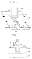
- Such light signal detection devices (shown in Fig. 1 have a microbridge type Josephson junction 192 which is formed of an oxide superconductor BaPb o.7 Bi 0.3 O3 (BPBO) thin film 191, and utilize changes in the critical current of the Josephson junction caused by the radiation illuminated on the junction by means of an optical fiber 190.
- a light-receiving portion is made of BPBO 191 having a critical temperature of about 13 K.
- liquid helium or the like must be used to operate the detecting device.
- the characteristics of the detecting device are dependent on those of the Josephson junction.
- the optical characteristics (e.g., spectral characteristics) of the device are determined by the spectral characteristics of the superconductor employed, i.e., wavelengths of the light to be detected are limited by the spectral characteristics of the superconductor, and detection of signals over a wide wavelength area is difficult.
- the above-described detecting device is operated as a recording device, a semiconductor memory, or a Josephson memory, since it is operated by means of an electrical signal, it is easily affected by electrical noises caused by the extension of wiring.
- the above-described conventional detecting device requires light having an intensity high enough to cause sufficient change in the critical current in the Josephson junction, which is difficult, and thus has a deteriorated sensitivity.
- the use of the same Josephson junction as a light-receiving portion and a light detecting portion causes variations in the characteristics of the device.
- Japanese Patent Laid-Open No. 50486/1989 discloses a light switching device (shown in Fig. 2 ) in which a PN semiconductor light signal sensing portion 204 is provided on a Josephson junction 203 of a superconductor 202 provided on a substrate 201.
- a light switching device shown in Fig. 2
- the semiconductor light signal sensing portion 204 is directly laid over the Josephson junction 203 as if it covers the entirety of the Josephson junction 203, the light signal detecting sensitivity of the Josephson junction 203 is deteriorated.
- the semiconductor light signal sensing portion 204 formed on the Josephson junction 203 is also small, making introduction of light into such a small area with a high degree of accuracy difficult.
- the present invention provides a light detecting device and a light detecting method intended as a solution to the conventional problems aforesaid.
- a light detecting device which comprises a signal input portion which generates a current when a light signal is input thereto, a signal detecting portion which employs a superconductor which detects the light signal upon injection of the generated current, and electrodes through which the generated current is injected into the superconductor.
- the light detecting device defined above can have a simple configuration and can exhibit excellent light signal detection sensitivity.
- a light detection method comprising the steps of: generating a current by inputting a light signal to a signal input portion; using electrodes to inject the generated current into a signal detecting portion including a superconductor; and detecting a change in electrical characteristics of said superconductor to detect the light signal.
- the first feature of the present invention is that a signal input portion to which a light signal is input and a signal detecting portion for detecting the light signal are provided as independent means. More specifically, the signal input portion and the signal detecting portion are basically formed of different materials and have separate functions.
- the second feature of the present invention resides in the form in which the signal input portion and the signal detecting portion are arranged.
- the signal input portion and the signal detecting portion are disposed separately, although they are electrically connected with each other by means of electrodes.
- the signal input portion and the signal detecting portion are provided as independent means, the overall configuration can be simplified, and the area of the signal input portion (the light-receiving portion) can be increased, eliminating the need for highly accurate positioning of the input light. Furthermore, since the signal input portion can be made of a material that can cope with light over a wide wavelength range limitation to the wavelength range of the input light is eliminated.
- the signal input portion and the signal detecting portion are separated from each other (are not in contact with each other), there is no deterioration in the signal detecting portion, e.g. a Josephson junction, which deterioration may be caused during the formation of the signal input portion, and excellent detection sensitivity can thus be obtained.
- the signal detecting portion e.g. a Josephson junction
- any material which is capable of coping with a light signal lying over a wide wavelength range, including, for example, any one of infrared light, visible light and ultraviolet light, and which is capable of generating a current or a voltage upon illumination of light, can be employed as the material of the signal input portion.
- photoconductive materials are desirable. Examples of photoconductive materials which generate a large amount of light current include InSb, Si, GaAs, a-Si, CdS, CdSe, and Ge.
- materials which generate a large amount of current due to the photovoltaic effect or the Dember effect can also be employed.
- Examples of materials which generate a photoelectromotive force include a PN junction made of Si or a-Si and a Schottky junction.
- any material, single crystal or polycrystal, which exhibits superconductivity can be used as the material of the signal detecting unit.
- materials having a high critical temperature are preferably employed. Suitable materials include those having a critical temperature higher than the boiling point of liquid nitrogen which is 77K, such as Y-Ba-Cu-O type ceramics, Bi-Sr-Ca-Cu-O type ceramics, and Tl-Ba-Ca-Cu-O type ceramics.
- the detecting device can be operated at temperatures lower than the critical temperature of the superconductor employed, it is preferable that the detecting device is operated at a temperature close to the critical temperature from the viewpoint of improving the detection sensitivity of an input signal.
- the signal detecting portion can have any form or configuration so long as its characteristics can be changed by injection of a current.
- suitable configurations include a microbridge Josephson junction, and a superconductor-insulator-super-conductor (SIS) Josephson junction.
- SIS superconductor-insulator-super-conductor
- a microbridge type is easier to manufacture.
- a SIS device exhibits a detection sensitivity which is higher than that of the microbridge type.
- any conductive material can be used as the material of the electrodes which electrically connect the signal input portion and the signal detecting portion in the aforementioned arrangement of the present invention.
- examples of such materials include metals such as Au (Au-Cr).
- Au Au-Cr
- the signal input portion and the signal detecting portion may be laid on top of each other with an electrode therebetween so long as they are not in direct contact with each other. In that case the signal input portion must be cooled when the signal detecting portion is cooled. Therefore, the arrangement in which the signal input portion is disposed outside of a cooling device in which the signal detecting portion is housed and in which the signal input portion and the signal detecting portion are connected by means of electrodes (conductors) is preferable because the signal input portion can be operated at room temperature and the operation efficiency can thus be improved. This also allows the use of materials, such as CdS or a-Si, which cannot be used at a very low temperature but are desirable from the viewpoint of improving sensitivity.
- a small heater for heating only the signal input portion may be provided in order to improve the detection sensitivity of the signal input portion.
- the devices according to the present invention may be integrated one-dimensionally or two-dimensionally to provide a line sensor or a plane sensor.
- a bias current which is slightly smaller in an amount than the critical current of the superconductor that forms the signal detecting portion be made to flow in the signal detecting portion from the viewpoint of further improving the detection sensitivity.
- the detecting device includes a superconductor for confining the magnetic field created by the generated current due to the Meissner effect.
- the superconductor which forms the signal detecting portion and the magnetic field confining superconductor may be the same or different.
- the magnetic field confining superconductor must be a superconductor whose critical magnetic field has a magnitude larger than that of the generated magnetic field.
- the present invention utilizes the following phenomenon: when the signal input portion made of, for example, a photoconductive material is exposed to radiation, electrons in the valence band are excited and take on a new energy level (in the conduction band). When the electrons in the conduction band are moved by an electric field applied thereto, a light current flows.
- the signal input portion 1 made of a photoconductive material or a material which generates a photoelectromotive force is exposed to light.
- the signal input portion 1 is made of a photoconductive material
- exposure of the signal input portion 1 to the radiation increases the excess charge carriers and causes the electrons in the valence band to be excited across the forbidden band into the conduction band.
- a light current flows in a conducting wire 2, and the generated current is injected into the signal detecting portion 4 (injected current I P ).
- Injection electrodes 2a and 2b are provided at the signal detecting portion 4.
- the signal input portion 1 is made of a material which generates a photoelectromotive force, such as a PN junction, d.c. voltage source 3 is not necessary, and the conductor 2 is made to form a continuous path for current.
- a bias current I B which is smaller than a Josephson current I J , is applied beforehand to the signal detecting portion 4 by means of a d.c. current source 5.
- the signal detecting portion 4 undergoes transition from a superconducting state to a voltage state.
- Such a switching operation is illustrated in the diagram of Fig. 4.
- the signal detecting portion includes a SIS device
- the operation of the SIS device follows a course of O - A - B - C - B - D - O.
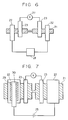
- Fig. 5 illustrates the concept of Example 1.
- a reference numeral 21 denotes a superconductor, 22; current injecting electrodes, 23; voltage measuring electrodes, 25; a photoconductive cell driving power source, 26; a photoconductive cell, and 27; a signal detecting voltmeter.
- an oxide superconductor YBa2Ca3O 7- ⁇ (0 ⁇ ⁇ ⁇ 0.5) was formed on a MgO substrate (not shown) by the magnetron sputtering technique or the like, and the obtained thin film was then processed by the photolithography technique or the like.
- the oxide superconductor had a belt-like shape having a thickness 500 nm (5000 ⁇ ) a width of 2 mm and a length of 5 mm.
- the microbridge portion had a width of 8 ⁇ m and a length of 12 ⁇ m.
- the current injecting electrodes 22 and the voltage measuring electrodes 23 of Cr, Au having a thickness of 100 nm (1000 ⁇ ) and a width of 50 ⁇ m were formed on the belt-like shape of the superconductor.
- the critical temperature of the superconductor was 88 K.
- the signal detecting portion of this detecting device was immersed in liquid nitrogen (77K), and 10 V was then applied to the photoconductive cell driving power source 25.
- the photoconductive cell 26 was not illuminated, 5 mA of dark current flowed in the photoconductive cell.
- the signal detecting voltmeter 27 pointed 0 V, which means that the superconductor was in a superconducting state.
- the signal detecting voltmeter 27 indicated 2 V. This means that illumination of the photoconductive cell caused a current having a value larger than the critical current value to flow in the superconductor 21, and caused the superconductor 21 to undergo transition to a nonsuperconducting state.
- Fig. 6 shows Example 2 of the present invention.
- the signal receiving portion of this detecting device employed a PN junction 28 which utilized the photovoltaic effect.
- the PN junction was not exposed to light in the liquid nitrogen, no voltage appeared.
- the PN junction 28 was illuminated in the same manner as in the case of Example 1, a voltage appeared. This means that the current which flowed in the superconductor 21 increased due to the photovoltaic effect, and that the superconductor underwent transition to a nonsuperconducting state.
- Light-receiving sensitivity will be improved by providing a small heater in the PN junction.
- Fig. 7 shows Example 3 of the present invention.
- a photoconductive thin film 29 (made of a- si) was formed on one of the current injecting electrodes 22 of the signal detecting portion, and an electrode 30 was then formed on the photoconductive thin film 29.
- the signal input portion and the signal detecting portion were formed as one unit.
- Fig. 8 shows Example 4 which employs the signal input portion made of Si and a Nb/Al-AlOx/Nb SIS device.
- an insulating film 38 (SiO2) was formed to a thickness of 100 nm (1000 ⁇ ) on half of a non-doped Si wafer substrate 37 (100 plane), and a lower electrode 36 (Nb), an insulating layer 31 (Al-AlOx), and an upper electrode 32 (Nb) were then formed on the insulating film 38 by the known technique to form an SIS device 33 having a junction area of 5 ⁇ m x 5 ⁇ m.
- the portion of the Si wafer 37 which was not covered by the insulating film 38 was processed using hydrofluoric acid, and comb electrodes 34 and 35 (Cr/Au) were then formed to a thickness of 150 nm (1500 ⁇ ) using a metal mask, as shown in Fig. 8.
- the length of the comb electrodes was 4 mm, the distance between the adjacent electrodes was 0.1 mm, and the light-receiving area of the comb electrodes was 0.05 cm2. In this way, ohmic contact was achieved between the Si and the Cr/Au.
- Fig. 9 shows a light detecting device which employs amorphous Si in the signal input portion and a Y-Ba-Cu-O/silver oxide/Pb SIS device.
- a lower electrode 41 was formed by depositing Y-Ba-Cu-O oxide superconductor to a thickness of 500 nm (5000 ⁇ ) on a MgO substrate (100 plane) 40 in argon and oxygen by means of the RF magnetron sputtering technique while maintaining the temperature of the substrate 40 to 550 °C, and an insulating layer (Ag/Ag2O) 42 was then formed to a thickness of 10 nm (100 ⁇ ) in argon and in vacuum while maintaining the temperature of the substrate to 100 °C.
- Ag was oxidized by introducing oxygen while heating to a temperature of 400 °C. Thereafter, a bridge pattern (41 and 42 in Fig.
- amorphous Si 44 was deposited to a thickness of 200nm (2000 ⁇ )in an area of 2 mm x 2 mm by the CVD process to form a signal input portion, and comb electrodes 45 and 46 (Cr/Au) were finally formed to a thickness of 50nm (500 ⁇ ).
- switching (0 mV to 20 mV) of the SIS device could be confirmed at a temperature of 4.2 K and with a bias current of 0.75 mA, 0.3 mW of illumination by means of a He-Ne laser (with a wavelength of 633 nm), and a comb electrode applied voltage of 10 V.
- the detecting device of Example 6 was manufactured in the same manner as Example 5 with the exception that a PN junction was formed by forming N type amorphous Si to a thickness of 150nm (1500 ⁇ ) and then by forming P type amorphous Si to a thickness of 150nm (1500 ⁇ ) on the N type amorphous Si, and that the upper electrode 43 (Pb) and the comb electrode 46 were short-circuited.
- a bias current of 0.8 mA was applied to this device at a temperature of 4.2 K and 3 mW of light was irradiated on the device by means of a He-Ne laser (with a wavelength of 633 nm), switching (0 mV to 20 mV) of the SIS device could be confirmed.
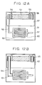
- Figs. 10A and 10B show the concept of and manufacture process of Example 7.
- a superconducting electrode 52 which served as a signal detecting portion was formed by depositing Y1Ba2Cu3O 7-x (0 ⁇ x ⁇ 0.5) superconducting thin film to a thickness of 500 nm (5000 ⁇ ) on a MgO substrate 51 by the magnetron sputtering process and then by conducting patterning on the superconducting thin film by the photolithography technique so that the thin film had a width of 20 ⁇ m and a length of 1 mm.
- a CdS thin film was deposited to a thickness of 1 ⁇ m in an area of 0.8 mm x 0.8 mm on the portion of the MgO substrate where no electrode was formed to form a signal input portion 53.
- a Pt thin film was deposited by the ion beam sputtering technique to form voltage detecting electrodes 54, 55, current injecting electrodes 56, 57 and 58, and comb electrodes 59 and 60.
- a MgO thin film was deposited to a thickness of 800 nm (8000 ⁇ )on the current injecting electrodes 56, 57 and 58 by the magnetron sputtering process to form insulating layers 61, 62 and 63, as shown in Fig. 10B, and magnetic field confining superconducting layers 64, 65 and 66 were then formed on the insulating layers 61, 62 and 63 in the same manner as that in which the superconducting electrode 52 was formed.
- Fig. 11 shows Example 8 in which two detecting devices having the same configuration as that employed in Example 7 are disposed very close to each other such that the distance between the superconducting electrodes 52 of the two detecting devices is 10 ⁇ m.
- Example 7 When one of the light input portions was illuminated in the same manner as in Example 7, the same results as those obtained in Example 7 were obtained in the illuminated light detecting device. The other light detecting device was not affected by this at all.
- Figs. 12A and 12B show Example 9 of the present invention.
- a MgO thin film was deposited to a thickness of 800 nm (8000 ⁇ ) on a Si substrate 51 which was not subjected to doping by the magnetron sputtering process to form an insulating layer 67, and a superconducting electrode 52 which served as a signal detecting portion was then formed by depositing Y1Ba2Cu3O 7-x (0 ⁇ x ⁇ 0.5) superconducting thin film to a thickness of 500 nm (5000 ⁇ ) on the MgO film 67 by the cluster ion beam deposition process and then by conducting patterning on the superconducting thin film so that the thin film had the same form as that of the superconducting electrode 52 employed in Example 7.
- voltage detecting electrodes 54, 55, current injecting electrodes 56, 57 and 58 (the electrode 58 being formed on the electrode 52), and comb electrodes 59 and 60 were formed.
- the comb electrodes 59 and 60 were formed directly on the photoconductive Si substrate to form a light input portion.
- MgO insulating layers 61 and 62 were formed on the electrodes 56 and 58, and magnetic field confining superconducting layers 64 and 65 were then formed on the insulating layers 61 and 62 in the same manner as that in Example 8, as shown in Fig. 12B.
- the thus-manufactured light detecting device exhibited the same light detection effect as that obtained by Example 8.
- Fig. 13 illustrates the concept of Example 10.
- a reference numeral 71 denotes a superconductor, 72; current injecting electrodes, 73; voltage measuring electrodes, 75; a photoconductive cell driving power source, 76; a photoconductive cell, and 77; a signal detecting voltmeter.
- an oxide superconductor YBa2Cu3O 7- ⁇ (0 ⁇ ⁇ ⁇ 0.5) was formed on a MgO substrate (not shown) by the magnetron sputtering technique or the like, and the obtained thin film was then processed by the photolithography technique or the like to form the belt-like superconductor 71.
- the superconductor 71 had a thickness of 500 nm (5000 ⁇ ), a width of 20 ⁇ m and a length of 5 mm.
- four Cr, Au electrodes were formed to a thickness of 100 nm (1000 ⁇ ) and in a width of 50 ⁇ m on the belt-like superconductor 71 to form the current injecting electrodes 72 and the voltage measuring electrodes 73.
- the critical temperature of the superconductor of the thus-arranged detecting device was 88 K.
- This detecting device was immersed in liquid nitrogen (77K), and 10 V was then applied to the photoconductive cell driving power source 75 to apply a bias current of 5 mA.
- the signal detecting voltmeter 77 pointed 0 V, which means that the superconductor was in a superconducting state.
- the signal detecting voltmeter 77 indicated 3 mV. This means that illumination of the photoconductive cell caused a current having a value larger than the critical current value to flow in the superconductor 71, thereby causing the superconductor 71 to undergo transition to a nonsuperconducting state.
- Fig. 14 shows Example 11 of the present invention.
- the signal input portion of this detecting device employed a PN junction 78 which utilized the photovoltaic effect.
- the PN junction 78 was not exposed to light in the liquid nitrogen, no voltage appeared.
- the PN junction 78 was illuminated in the same manner as in the case of Example 10, a voltage appeared. This means that the current which flowed in the superconductor 71 increased due to the photovoltaic effect and that the superconductor underwent transition to a nonsuperconducting state.
- Light-receiving sensitivity will be improved by providing a small heater in the PN junction, as the photoconductive cell 76 was employed at room temperature in Example 10.
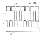
- Fig. 15 shows Example 12 in which the light detecting devices shown in Fig. 14 were arranged in an array.
- Reference numerals 71 denote superconducting thin wires aligned on a straight line. Each of the superconducting thin wires 71 has a thickness of 0.5 ⁇ m, a width of 15 ⁇ m and a length of 50 ⁇ m.
- a reference numeral 79 denotes a voltage measuring circuit which indicates the voltage of each of the superconducting thin wires.
- a series of light-receiving portions 78 (PN junctions) are disposed separately from the superconducting wires so that temperature-setting can be separately conducted on the superconducting portions 71 and the light-receiving portions 78. When 10 m lux of light was illuminated on the left half of this array, a voltage appeared on the left half. This means that this array can be used as a line sensor.
Description
- The present invention relates to a light detecting device and a light detection method which employ a superconductor, for example, a light detecting device and a light detection method which employ a Josephson junction .
- Signal detecting devices which utilize a superconductor, particularly, light signal detecting devices which utilize a superconductor, have been known [Japanese Journal of Applied Physics vol. 23 L333 (1984). Such light signal detection devices (shown in Fig. 1 have a microbridge type Josephson
junction 192 which is formed of an oxide superconductor BaPbo.7Bi0.3O₃ (BPBO)thin film 191, and utilize changes in the critical current of the Josephson junction caused by the radiation illuminated on the junction by means of anoptical fiber 190. In the above-described detection device, a light-receiving portion is made ofBPBO 191 having a critical temperature of about 13 K. In other words, liquid helium or the like must be used to operate the detecting device. Furthermore, the characteristics of the detecting device are dependent on those of the Josephson junction. - In the above-described conventional detecting device, the optical characteristics (e.g., spectral characteristics) of the device are determined by the spectral characteristics of the superconductor employed, i.e., wavelengths of the light to be detected are limited by the spectral characteristics of the superconductor, and detection of signals over a wide wavelength area is difficult.
- Furthermore, in a case where the above-described detecting device is operated as a recording device, a semiconductor memory, or a Josephson memory, since it is operated by means of an electrical signal, it is easily affected by electrical noises caused by the extension of wiring.
- Furthermore, in a case where the above-described detecting device is used together with a large number of other detecting devices, as in an image sensor, it is difficult to compensate for variations in the characteristics of the individual detecting devices caused during the manufacture thereof.
- Furthermore, since the area of the junction to which radiation is irradiated is limited, highly accurate positioning is required.
- The above-described conventional detecting device requires light having an intensity high enough to cause sufficient change in the critical current in the Josephson junction, which is difficult, and thus has a deteriorated sensitivity.
- Furthermore, the use of the same Josephson junction as a light-receiving portion and a light detecting portion causes variations in the characteristics of the device.
- Japanese Patent Laid-Open No. 50486/1989 discloses a light switching device (shown in Fig. 2 ) in which a PN semiconductor light
signal sensing portion 204 is provided on a Josephsonjunction 203 of asuperconductor 202 provided on asubstrate 201. However, in such a light switching device, since the semiconductor lightsignal sensing portion 204 is directly laid over the Josephsonjunction 203 as if it covers the entirety of the Josephsonjunction 203, the light signal detecting sensitivity of the Josephsonjunction 203 is deteriorated. Furthermore, since the area of the Josephsonjunction 203 is very small, the semiconductor lightsignal sensing portion 204 formed on the Josephsonjunction 203 is also small, making introduction of light into such a small area with a high degree of accuracy difficult. - The present invention provides a light detecting device and a light detecting method intended as a solution to the conventional problems aforesaid.
- In accordance with one aspect of the present invention there is provided a light detecting device which comprises a signal input portion which generates a current when a light signal is input thereto, a signal detecting portion which employs a superconductor which detects the light signal upon injection of the generated current, and electrodes through which the generated current is injected into the superconductor.
- The light detecting device defined above can have a simple configuration and can exhibit excellent light signal detection sensitivity.
- In accordance with another aspect of the invention there is provided a light detection method comprising the steps of:
generating a current by inputting a light signal to a signal input portion;
using electrodes to inject the generated current into a signal detecting portion including a superconductor; and
detecting a change in electrical characteristics of said superconductor to detect the light signal. - In the accompanying drawings:
- Figs. 1 and 2 are schematic views showing conventional detecting devices;
- Figs. 3 and 4 illustrate the principle of the operation of the present invention; and
- Figs. 5 to 9, 10 (A) and (B), 11, 12 (A) and (B), 13, 14 and 15 are respectively schematic views of embodiments according to the present invention.
- To better facilitate an understanding of this, preferred embodiments will be described in detail hereinbelow and reference will be made to the drawings. The following description is intended by way of example only.
- The first feature of the present invention is that a signal input portion to which a light signal is input and a signal detecting portion for detecting the light signal are provided as independent means. More specifically, the signal input portion and the signal detecting portion are basically formed of different materials and have separate functions.
- The second feature of the present invention resides in the form in which the signal input portion and the signal detecting portion are arranged. In the arrangement defined, the signal input portion and the signal detecting portion are disposed separately, although they are electrically connected with each other by means of electrodes.
- In the present invention, since the signal input portion and the signal detecting portion are provided as independent means, the overall configuration can be simplified, and the area of the signal input portion (the light-receiving portion) can be increased, eliminating the need for highly accurate positioning of the input light.
Furthermore, since the signal input portion can be made of a material that can cope with light over a wide wavelength range limitation to the wavelength range of the input light is eliminated. - Furthermore, in the present invention, since the signal input portion and the signal detecting portion are separated from each other (are not in contact with each other), there is no deterioration in the signal detecting portion, e.g. a Josephson junction, which deterioration may be caused during the formation of the signal input portion, and excellent detection sensitivity can thus be obtained.
- In embodying the present invention, any material, which is capable of coping with a light signal lying over a wide wavelength range, including, for example, any one of infrared light, visible light and ultraviolet light, and which is capable of generating a current or a voltage upon illumination of light, can be employed as the material of the signal input portion. In particular, photoconductive materials are desirable. Examples of photoconductive materials which generate a large amount of light current include InSb, Si, GaAs, a-Si, CdS, CdSe, and Ge.
- In addition to the materials mentioned above, materials which generate a large amount of current due to the photovoltaic effect or the Dember effect can also be employed.
- Examples of materials which generate a photoelectromotive force include a PN junction made of Si or a-Si and a Schottky junction.
- Any material, single crystal or polycrystal, which exhibits superconductivity can be used as the material of the signal detecting unit. In terms of the operation of a detecting device at a higher temperature, materials having a high critical temperature are preferably employed. Suitable materials include those having a critical temperature higher than the boiling point of liquid nitrogen which is 77K, such as Y-Ba-Cu-O type ceramics, Bi-Sr-Ca-Cu-O type ceramics, and Tℓ-Ba-Ca-Cu-O type ceramics.
- Although the detecting device can be operated at temperatures lower than the critical temperature of the superconductor employed, it is preferable that the detecting device is operated at a temperature close to the critical temperature from the viewpoint of improving the detection sensitivity of an input signal.
- The signal detecting portion can have any form or configuration so long as its characteristics can be changed by injection of a current. Examples of suitable configurations include a microbridge Josephson junction, and a superconductor-insulator-super-conductor (SIS) Josephson junction.
- In a case where a Josephson junction is employed as the signal detecting portion, a microbridge type is easier to manufacture. However, a SIS device exhibits a detection sensitivity which is higher than that of the microbridge type.
- Any conductive material can be used as the material of the electrodes which electrically connect the signal input portion and the signal detecting portion in the aforementioned arrangement of the present invention. Examples of such materials include metals such as Au (Au-Cr). There is no limitation to the form of the electrode.
- In the aforementioned arrangement, the signal input portion and the signal detecting portion may be laid on top of each other with an electrode therebetween so long as they are not in direct contact with each other. In that case the signal input portion must be cooled when the signal detecting portion is cooled. Therefore, the arrangement in which the signal input portion is disposed outside of a cooling device in which the signal detecting portion is housed and in which the signal input portion and the signal detecting portion are connected by means of electrodes (conductors) is preferable because the signal input portion can be operated at room temperature and the operation efficiency can thus be improved. This also allows the use of materials, such as CdS or a-Si, which cannot be used at a very low temperature but are desirable from the viewpoint of improving sensitivity.
- In the present invention, a small heater for heating only the signal input portion may be provided in order to improve the detection sensitivity of the signal input portion. Furthermore, the devices according to the present invention may be integrated one-dimensionally or two-dimensionally to provide a line sensor or a plane sensor.
- Furthermore, in the present invention, it is preferable that a bias current which is slightly smaller in an amount than the critical current of the superconductor that forms the signal detecting portion be made to flow in the signal detecting portion from the viewpoint of further improving the detection sensitivity.
- In a preferred form, the detecting device according to the present invention includes a superconductor for confining the magnetic field created by the generated current due to the Meissner effect.
- When the magnetic field confining superconductor provided separately from the aforementioned signal detecting superconductor in such a manner that it covers at least the signal detecting portion is in a state in which the Meissner effect is occurring, leakage of the generated magnetic field or adverse effect of the noises on the detector can be restricted.
- This leads to improvement of the detection efficiency of the detector, and enables the concurrent use of a plurality of detectors.
- The superconductor which forms the signal detecting portion and the magnetic field confining superconductor may be the same or different. However, the magnetic field confining superconductor must be a superconductor whose critical magnetic field has a magnitude larger than that of the generated magnetic field.
- Next, the principle of the operation of the present invention will be described.
- The present invention utilizes the following phenomenon: when the signal input portion made of, for example, a photoconductive material is exposed to radiation, electrons in the valence band are excited and take on a new energy level (in the conduction band). When the electrons in the conduction band are moved by an electric field applied thereto, a light current flows.
- When a current which is made to flow in a superconductor exceeds the critical current value of the superconductor, the superconductor undergoes a transition from the superconducting phase, and a voltage appears.
- In Fig. 3, first, the signal input portion 1 made of a photoconductive material or a material which generates a photoelectromotive force is exposed to light.
- In a case where the signal input portion 1 is made of a photoconductive material, exposure of the signal input portion 1 to the radiation increases the excess charge carriers and causes the electrons in the valence band to be excited across the forbidden band into the conduction band. When the electrons in the conduction band are moved by the electric field applied thereto by a d.c.
voltage source 3, a light current flows in aconducting wire 2, and the generated current is injected into the signal detecting portion 4 (injected current IP). -
Injection electrodes signal detecting portion 4. - In a case where the signal input portion 1 is made of a material which generates a photoelectromotive force, such as a PN junction, d.c.
voltage source 3 is not necessary, and theconductor 2 is made to form a continuous path for current. - A bias current IB, which is smaller than a Josephson current IJ, is applied beforehand to the
signal detecting portion 4 by means of a d.c.current source 5. - When

signal detecting portion 4 undergoes transition from a superconducting state to a voltage state. - Such a switching operation is illustrated in the diagram of Fig. 4. When the signal detecting portion includes a SIS device, the operation of the SIS device follows a course of O - A - B - C - B - D - O. When IP = 0, the SIS device is at the operation point X (voltage = 0), and when IP ≠ 0 and


- The above-described present invention has the following advantages.
- 1. When compared with the conventional device (in which, for example, a Josephson junction is exposed to radiation), positioning of a light signal onto the detecting device is facilitated, i.e., a signal can be input to an input portion (signal receiving portion) having an arbitrary size.
- 2. Since the range of selection of the material of the optical signal input portion (light-receiving portion) is widened, signals can be detected over a wider wavelength range.
- 3. Compared with a conventional device (in the conventional Josephson junction, the detection characteristics are determined by the junction characteristics, and there are variations in the characteristics of the individual devices of a multi-structure sensor), reproducibility and reliability are improved and variations in the characteristics are lessened These facilitate integration of detecting devices.
- 4. If the superconductor which forms the detecting portion is operated at a temperature closer to the critical temperature thereof, detection sensitivity can be improved.
- 5. In a case where the hysteresis inherent in a SIS device is utilized, the resulting light detecting device exhibits a high detection sensitivity which enables it to function as a storage device. In a case where the light detecting device is operated as a storage device, since a signal is light, substrate wiring can be reduced, resulting in a detection device which withstands electrical and magnetic noises well.
- 6. Since the magnetic field created by the current generated by radiation input is confined due to the Meissner effect of a superconductor, detection sensitivity can be improved, and mutual influence between the detectors can be eliminated. These enable integration of the detection devices and increase detection efficiency.
- 7. In the case where a signal detecting portion is disposed within a cooler while a signal input portion is disposed outside of the cooler, the signal input portion can be operated at room temperature and the operation efficiency can be improved.
- The present invention will now be described below by way of example.
- Fig. 5 illustrates the concept of Example 1. In Fig.5, a
reference numeral 21 denotes a superconductor, 22; current injecting electrodes, 23; voltage measuring electrodes, 25; a photoconductive cell driving power source, 26; a photoconductive cell, and 27; a signal detecting voltmeter. - First, an oxide superconductor YBa₂Ca₃O7-δ (0 ≦ δ ≦ 0.5) was formed on a MgO substrate (not shown) by the magnetron sputtering technique or the like, and the obtained thin film was then processed by the photolithography technique or the like. In this Example, the oxide superconductor had a belt-like shape having a thickness 500 nm (5000 Å) a width of 2 mm and a length of 5 mm. The microbridge portion had a width of 8 µm and a length of 12 µm. Next, the
current injecting electrodes 22 and thevoltage measuring electrodes 23 of Cr, Au having a thickness of 100 nm (1000 Å) and a width of 50 µm were formed on the belt-like shape of the superconductor. - The critical temperature of the superconductor was 88 K. The signal detecting portion of this detecting device was immersed in liquid nitrogen (77K), and 10 V was then applied to the photoconductive cell driving
power source 25. When thephotoconductive cell 26 was not illuminated, 5 mA of dark current flowed in the photoconductive cell. Also, thesignal detecting voltmeter 27 pointed 0 V, which means that the superconductor was in a superconducting state. When 5 mW of light was irradiated on thephotoconductive cell 26 by means of a He-Ne laser at room temperature, thesignal detecting voltmeter 27 indicated 2 V. This means that illumination of the photoconductive cell caused a current having a value larger than the critical current value to flow in thesuperconductor 21, and caused thesuperconductor 21 to undergo transition to a nonsuperconducting state. - Fig. 6 shows Example 2 of the present invention. The signal receiving portion of this detecting device employed a
PN junction 28 which utilized the photovoltaic effect. When the PN junction was not exposed to light in the liquid nitrogen, no voltage appeared. When thePN junction 28 was illuminated in the same manner as in the case of Example 1, a voltage appeared. This means that the current which flowed in thesuperconductor 21 increased due to the photovoltaic effect, and that the superconductor underwent transition to a nonsuperconducting state. - Light-receiving sensitivity will be improved by providing a small heater in the PN junction.
- Fig. 7 shows Example 3 of the present invention. In this detecting device, a photoconductive thin film 29 (made of a- si) was formed on one of the
current injecting electrodes 22 of the signal detecting portion, and anelectrode 30 was then formed on the photoconductivethin film 29. In other words, the signal input portion and the signal detecting portion were formed as one unit. When the same measurement as that conducted in Example 1 was conducted on this detecting device, the same results were obtained. - Fig. 8 shows Example 4 which employs the signal input portion made of Si and a Nb/Aℓ-AℓOx/Nb SIS device.
- First, an insulating film 38 (SiO₂) was formed to a thickness of 100 nm (1000 Å) on half of a non-doped Si wafer substrate 37 (100 plane), and a lower electrode 36 (Nb), an insulating layer 31 (Aℓ-AℓOx), and an upper electrode 32 (Nb) were then formed on the insulating
film 38 by the known technique to form an SIS device 33 having a junction area of 5 µm x 5 µm. Next, the portion of theSi wafer 37 which was not covered by the insulatingfilm 38 was processed using hydrofluoric acid, and combelectrodes 34 and 35 (Cr/Au) were then formed to a thickness of 150 nm (1500 Å) using a metal mask, as shown in Fig. 8. The length of the comb electrodes was 4 mm, the distance between the adjacent electrodes was 0.1 mm, and the light-receiving area of the comb electrodes was 0.05 cm². In this way, ohmic contact was achieved between the Si and the Cr/Au. When light response of the thus-manufactured light detecting device was estimated, switching of the SIS device (0 mV to 2,8 mV) could be confirmed at a temperature of 4.2 K with a bias current of 1.2 mA, 0.3 mW of illumination by means of a He-Ne laser (with a wavelength of 633 nm), and a comb electrode applied voltage of 10 V. - Fig. 9 shows a light detecting device which employs amorphous Si in the signal input portion and a Y-Ba-Cu-O/silver oxide/Pb SIS device.
- First, a
lower electrode 41 was formed by depositing Y-Ba-Cu-O oxide superconductor to a thickness of 500 nm (5000Å) on a MgO substrate (100 plane) 40 in argon and oxygen by means of the RF magnetron sputtering technique while maintaining the temperature of thesubstrate 40 to 550 °C, and an insulating layer (Ag/Ag₂O) 42 was then formed to a thickness of 10 nm (100 Å) in argon and in vacuum while maintaining the temperature of the substrate to 100 °C. Next, Ag was oxidized by introducing oxygen while heating to a temperature of 400 °C. Thereafter, a bridge pattern (41 and 42 in Fig. 9) having a width of 10 µm was formed by the photolithography process. Next, an upper electrode 43 (Pb) was deposited to a thickness of 50 nm (500 Å) using a metal mask. The portion of theupper electrode 43 which was laid on the bridge pattern had a width of 100 µm and a junction area of 100 µm x 10 µm. The effective area was an order of magnitude less due to non-uniformity of the Ag oxide film. Next,amorphous Si 44 was deposited to a thickness of 200nm (2000 Å)in an area of 2 mm x 2 mm by the CVD process to form a signal input portion, and combelectrodes 45 and 46 (Cr/Au) were finally formed to a thickness of 50nm (500Å). When light response of the light detecting device manufactured in the manner described above was estimated, switching (0 mV to 20 mV) of the SIS device could be confirmed at a temperature of 4.2 K and with a bias current of 0.75 mA, 0.3 mW of illumination by means of a He-Ne laser (with a wavelength of 633 nm), and a comb electrode applied voltage of 10 V. - The detecting device of Example 6 was manufactured in the same manner as Example 5 with the exception that a PN junction was formed by forming N type amorphous Si to a thickness of 150nm (1500 Å) and then by forming P type amorphous Si to a thickness of 150nm (1500 Å) on the N type amorphous Si, and that the upper electrode 43 (Pb) and the
comb electrode 46 were short-circuited. When a bias current of 0.8 mA was applied to this device at a temperature of 4.2 K and 3 mW of light was irradiated on the device by means of a He-Ne laser (with a wavelength of 633 nm), switching (0 mV to 20 mV) of the SIS device could be confirmed. - Figs. 10A and 10B show the concept of and manufacture process of Example 7.
- First, a
superconducting electrode 52 which served as a signal detecting portion was formed by depositing Y₁Ba₂Cu₃O7-x (0 ≦ x ≦ 0.5) superconducting thin film to a thickness of 500 nm (5000 Å) on aMgO substrate 51 by the magnetron sputtering process and then by conducting patterning on the superconducting thin film by the photolithography technique so that the thin film had a width of 20 µm and a length of 1 mm. Next, a CdS thin film was deposited to a thickness of 1 µm in an area of 0.8 mm x 0.8 mm on the portion of the MgO substrate where no electrode was formed to form asignal input portion 53. Next, a Pt thin film was deposited by the ion beam sputtering technique to formvoltage detecting electrodes current injecting electrodes electrodes current injecting electrodes layers superconducting layers layers superconducting electrode 52 was formed. - In the thus-manufactured detecting device, all the superconductors were in a superconducting state at a temperature of 82 K. The light detecting device was cooled to 77 K by immersing it in liquid nitrogen.
- When 10 V was applied between the
current injecting electrodes signal input portion 53, no voltage appeared between thevoltage detecting electrodes signal input portion 53 by means of a He-Ne laser and the current which flowed in thesuperconducting electrode 52 thereby exceeded the critical current value thereof, thesuperconducting electrode 52 underwent a transition to a voltage state, and 10 mV of voltage thus appeared. - Fig. 11 shows Example 8 in which two detecting devices having the same configuration as that employed in Example 7 are disposed very close to each other such that the distance between the
superconducting electrodes 52 of the two detecting devices is 10 µm. - When one of the light input portions was illuminated in the same manner as in Example 7, the same results as those obtained in Example 7 were obtained in the illuminated light detecting device. The other light detecting device was not affected by this at all.
- Figs. 12A and 12B show Example 9 of the present invention.
- First, a MgO thin film was deposited to a thickness of 800 nm (8000Å) on a
Si substrate 51 which was not subjected to doping by the magnetron sputtering process to form an insulatinglayer 67, and asuperconducting electrode 52 which served as a signal detecting portion was then formed by depositing Y₁Ba₂Cu₃O7-x (0 ≦ x ≦ 0.5) superconducting thin film to a thickness of 500 nm (5000 Å) on theMgO film 67 by the cluster ion beam deposition process and then by conducting patterning on the superconducting thin film so that the thin film had the same form as that of thesuperconducting electrode 52 employed in Example 7. Next,voltage detecting electrodes current injecting electrodes electrode 58 being formed on the electrode 52), and combelectrodes comb electrodes MgO insulating layers electrodes superconducting layers layers - The thus-manufactured light detecting device exhibited the same light detection effect as that obtained by Example 8.
- Fig. 13 illustrates the concept of Example 10. In Fig. 13, a
reference numeral 71 denotes a superconductor, 72; current injecting electrodes, 73; voltage measuring electrodes, 75; a photoconductive cell driving power source, 76; a photoconductive cell, and 77; a signal detecting voltmeter. - First, an oxide superconductor YBa₂Cu₃O7-δ (0 ≦ δ ≦ 0.5) was formed on a MgO substrate (not shown) by the magnetron sputtering technique or the like, and the obtained thin film was then processed by the photolithography technique or the like to form the belt-
like superconductor 71. In this Example, thesuperconductor 71 had a thickness of 500 nm (5000Å), a width of 20 µm and a length of 5 mm. Next, four Cr, Au electrodes were formed to a thickness of 100 nm (1000 Å) and in a width of 50 µm on the belt-like superconductor 71 to form thecurrent injecting electrodes 72 and thevoltage measuring electrodes 73. - The critical temperature of the superconductor of the thus-arranged detecting device was 88 K. This detecting device was immersed in liquid nitrogen (77K), and 10 V was then applied to the photoconductive cell driving
power source 75 to apply a bias current of 5 mA. When thephotoconductive cell 76 was placed at room temperature and no illumination was conducted on thecell 76, thesignal detecting voltmeter 77 pointed 0 V, which means that the superconductor was in a superconducting state. When 5 mW of light was irradiated on thephotoconductive cell 76 by means of a He-Ne laser, thesignal detecting voltmeter 77 indicated 3 mV. This means that illumination of the photoconductive cell caused a current having a value larger than the critical current value to flow in thesuperconductor 71, thereby causing thesuperconductor 71 to undergo transition to a nonsuperconducting state. - Fig. 14 shows Example 11 of the present invention. The signal input portion of this detecting device employed a
PN junction 78 which utilized the photovoltaic effect. When thePN junction 78 was not exposed to light in the liquid nitrogen, no voltage appeared. When thePN junction 78 was illuminated in the same manner as in the case of Example 10, a voltage appeared. This means that the current which flowed in thesuperconductor 71 increased due to the photovoltaic effect and that the superconductor underwent transition to a nonsuperconducting state. - Light-receiving sensitivity will be improved by providing a small heater in the PN junction, as the
photoconductive cell 76 was employed at room temperature in Example 10. - Fig. 15 shows Example 12 in which the light detecting devices shown in Fig. 14 were arranged in an array.
Reference numerals 71 denote superconducting thin wires aligned on a straight line. Each of the superconductingthin wires 71 has a thickness of 0.5 µm, a width of 15 µm and a length of 50 µm. Areference numeral 79 denotes a voltage measuring circuit which indicates the voltage of each of the superconducting thin wires. A series of light-receiving portions 78 (PN junctions) are disposed separately from the superconducting wires so that temperature-setting can be separately conducted on thesuperconducting portions 71 and the light-receivingportions 78. When 10 m lux of light was illuminated on the left half of this array, a voltage appeared on the left half. This means that this array can be used as a line sensor.
Claims (8)
- A light detecting device comprising:
a signal input portion (1) which generates a current upon input of a light signal;
a separate signal detecting portion (4) including a superconductor which detects the light signal upon injection of the generated current; and
electrodes (2a,2b) by which the generated current is injected into said superconductor. - A light detecting device according to claim 1, wherein said signal detecting portion (4) includes a microbridge type Josephson junction (21).
- A light detecting device according to claim 1, wherein said signal detecting portion (4) includes a superconductor-insulator-superconductor Josephson junction (33).
- A light detecting device according to claim 1, wherein said signal input portion (1) is made of a selected one of photoconducting material and a material which generates a photoelectromotive force.
- A light detecting device according to claim 1, further comprising a magnetic field confining superconductor (64,65,66) for confining a magnetic field created by the generated current due to the Meissner effect.
- A light detecting device according to claim 1, further comprising a cooler for cooling at least the signal detecting portion (4).
- A light detecting device according to claim 6, wherein said signal detecting portion (4) is disposed within said cooler while said signal input portion (1) is disposed outside of said cooler.
- A light detection method, comprising the steps of:
generating a current by inputting a light signal to a signal input portion;
using electrodes to inject the generated current into a separate signal detecting portion including a superconductor; and
detecting a change in electrical characteristics of said superconductor to detect the light signal.
Priority Applications (1)
| Application Number | Priority Date | Filing Date | Title |
|---|---|---|---|
| EP93203066A EP0590738B1 (en) | 1989-07-05 | 1990-07-04 | Light detecting device and light detecting method using a superconductor |
Applications Claiming Priority (18)
| Application Number | Priority Date | Filing Date | Title |
|---|---|---|---|
| JP1171917A JP2737003B2 (en) | 1989-07-05 | 1989-07-05 | Signal detection method |
| JP1171918A JP2737004B2 (en) | 1989-07-05 | 1989-07-05 | Signal detection method |
| JP171917/89 | 1989-07-05 | ||
| JP171918/89 | 1989-07-05 | ||
| JP180286/89 | 1989-07-14 | ||
| JP1180286A JP2737007B2 (en) | 1989-07-14 | 1989-07-14 | Signal detector |
| JP1180285A JP2737006B2 (en) | 1989-07-14 | 1989-07-14 | Signal detector |
| JP180285/89 | 1989-07-14 | ||
| JP1184424A JP2737008B2 (en) | 1989-07-19 | 1989-07-19 | Photodetector |
| JP184425/89 | 1989-07-19 | ||
| JP1184425A JP2896788B2 (en) | 1989-07-19 | 1989-07-19 | Photodetector |
| JP184424/89 | 1989-07-19 | ||
| JP192528/89 | 1989-07-27 | ||
| JP1192529A JP2759508B2 (en) | 1989-07-27 | 1989-07-27 | Photo detector |
| JP1192528A JP2715320B2 (en) | 1989-07-27 | 1989-07-27 | Photodetector |
| JP192530/89 | 1989-07-27 | ||
| JP1192530A JP2715321B2 (en) | 1989-07-27 | 1989-07-27 | Photo detector |
| JP192529/89 | 1989-07-27 |
Related Child Applications (1)
| Application Number | Title | Priority Date | Filing Date |
|---|---|---|---|
| EP93203066.1 Division-Into | 1993-11-02 |
Publications (3)
| Publication Number | Publication Date |
|---|---|
| EP0407166A2 EP0407166A2 (en) | 1991-01-09 |
| EP0407166A3 EP0407166A3 (en) | 1991-08-07 |
| EP0407166B1 true EP0407166B1 (en) | 1994-05-25 |
Family
ID=27577522
Family Applications (2)
| Application Number | Title | Priority Date | Filing Date |
|---|---|---|---|
| EP90307302A Expired - Lifetime EP0407166B1 (en) | 1989-07-05 | 1990-07-04 | Light detecting device and light detection method |
| EP93203066A Expired - Lifetime EP0590738B1 (en) | 1989-07-05 | 1990-07-04 | Light detecting device and light detecting method using a superconductor |
Family Applications After (1)
| Application Number | Title | Priority Date | Filing Date |
|---|---|---|---|
| EP93203066A Expired - Lifetime EP0590738B1 (en) | 1989-07-05 | 1990-07-04 | Light detecting device and light detecting method using a superconductor |
Country Status (3)
| Country | Link |
|---|---|
| US (1) | US5155093A (en) |
| EP (2) | EP0407166B1 (en) |
| DE (2) | DE69031501T2 (en) |
Families Citing this family (26)
| Publication number | Priority date | Publication date | Assignee | Title |
|---|---|---|---|---|
| US6584245B1 (en) * | 1996-05-06 | 2003-06-24 | Teracomm Research, Inc | High speed data link including a superconductive plate assembly for use in a data transmission scheme and method |
| US5768002A (en) * | 1996-05-06 | 1998-06-16 | Puzey; Kenneth A. | Light modulation system including a superconductive plate assembly for use in a data transmission scheme and method |
| JPH11346010A (en) * | 1998-03-30 | 1999-12-14 | Sharp Corp | Photodetector |
| JP2002074936A (en) | 2000-08-31 | 2002-03-15 | Canon Inc | Magnetic device |
| JP2002084019A (en) | 2000-09-08 | 2002-03-22 | Canon Inc | Magnetic device and solid magnetic storage device |
| US6738548B2 (en) * | 2001-04-19 | 2004-05-18 | Teracomm Research, Inc | Reduced four-wave mixing optical fiber for wavelength-division multiplexing |
| DE10221442B4 (en) * | 2002-05-15 | 2005-09-22 | Xignal Technologies Ag | Inductive element of an integrated circuit |
| US7273479B2 (en) * | 2003-01-15 | 2007-09-25 | Cryodynamics, Llc | Methods and systems for cryogenic cooling |
| US7083612B2 (en) | 2003-01-15 | 2006-08-01 | Cryodynamics, Llc | Cryotherapy system |
| US7410484B2 (en) | 2003-01-15 | 2008-08-12 | Cryodynamics, Llc | Cryotherapy probe |
| DE102004045105A1 (en) * | 2004-03-19 | 2005-10-13 | Daimlerchrysler Ag | Use of a photovoltaic element as sensor for function control of transmitters in the infrared range |
| JP2006079846A (en) * | 2004-09-07 | 2006-03-23 | Canon Inc | Cross section evaluation device of sample and cross section evaluation method of sample |
| US8571614B1 (en) | 2009-10-12 | 2013-10-29 | Hypres, Inc. | Low-power biasing networks for superconducting integrated circuits |
| CA2922970C (en) | 2013-09-24 | 2022-09-13 | Adagio Medical, Inc. | Endovascular near critical fluid based cryoablation catheter and related methods |
| US10617459B2 (en) | 2014-04-17 | 2020-04-14 | Adagio Medical, Inc. | Endovascular near critical fluid based cryoablation catheter having plurality of preformed treatment shapes |
| EP3217903A4 (en) | 2014-11-13 | 2018-05-30 | Adagio Medical, Inc. | Pressure modulated cryoablation system and related methods |
| US9945728B2 (en) | 2015-04-03 | 2018-04-17 | Raytheon Bbn Technologies Corp. | Graphene-based infrared single photon detector |
| US10222416B1 (en) | 2015-04-14 | 2019-03-05 | Hypres, Inc. | System and method for array diagnostics in superconducting integrated circuit |
| US9869592B2 (en) | 2015-06-17 | 2018-01-16 | Raytheon Bbn Technologies Corp. | Graphene-based bolometer |
| US9933310B2 (en) | 2015-06-17 | 2018-04-03 | Raytheon Bbn Technologies Corp. | Graphene-based infrared bolometer |
| US9577176B1 (en) * | 2015-06-18 | 2017-02-21 | Raytheon Bbn Technologies Corp. | Josephson junction readout for graphene-based single photon detector |
| US9799817B2 (en) | 2015-06-18 | 2017-10-24 | Raytheon Bbn Technologies Corp. | Josephson junction readout for graphene-based single photon detector |
| WO2017048965A1 (en) | 2015-09-18 | 2017-03-23 | Adagio Medical Inc. | Tissue contact verification system |
| WO2017095756A1 (en) | 2015-11-30 | 2017-06-08 | Adagio Medical, Inc. | Ablation method for creating elongate continuous lesions enclosing multiple vessel entries |
| JP2020532408A (en) | 2017-09-05 | 2020-11-12 | アダージョ メディカル インコーポレイテッドAdagio Medical,Inc. | Ablation catheter with shape memory stylet |
| US11751930B2 (en) | 2018-01-10 | 2023-09-12 | Adagio Medical, Inc. | Cryoablation element with conductive liner |
Family Cites Families (13)
| Publication number | Priority date | Publication date | Assignee | Title |
|---|---|---|---|---|
| US4334158A (en) * | 1980-06-06 | 1982-06-08 | International Business Machines Corporation | Superconducting switch and amplifier device |
| EP0081007B1 (en) * | 1981-12-09 | 1986-08-20 | International Business Machines Corporation | Superconducting tunnel junction device |
| JPS59210677A (en) * | 1983-05-14 | 1984-11-29 | Nippon Telegr & Teleph Corp <Ntt> | Photodetecting element using josephson junction |
| DD248870A1 (en) * | 1986-02-03 | 1987-08-19 | Univ Schiller Jena | ARRANGEMENT FOR HIGHLY SENSITIVE DETECTION OF ELECTROMAGNETIC RADIATION WITH SUPERCONDUCTIVE QUANTUM INTERFERENCE DETECTOR |
| US4843446A (en) * | 1986-02-27 | 1989-06-27 | Hitachi, Ltd. | Superconducting photodetector |
| EP0301962B1 (en) * | 1987-07-27 | 1994-04-20 | Sumitomo Electric Industries Limited | A superconducting thin film and a method for preparing the same |
| US5011818A (en) * | 1987-07-29 | 1991-04-30 | Sharp Kabushiki Kaisha | Sensing a magnetic field with a super conductive material that exhibits magneto resistive properties |
| JPS6450486A (en) * | 1987-08-20 | 1989-02-27 | Mitsubishi Electric Corp | Optical switch element |
| US4814598A (en) * | 1987-09-03 | 1989-03-21 | Hypres, Inc. | Optical wavelength analyzer and image processing system utilizing Josephson junctions |
| JPS6488318A (en) * | 1987-09-30 | 1989-04-03 | Nec Corp | Superconductive photodetector having memory function |
| US4990487A (en) * | 1988-03-11 | 1991-02-05 | The University Of Tokyo | Superconductive optoelectronic devices |
| US4970395A (en) * | 1988-12-23 | 1990-11-13 | Honeywell Inc. | Wavelength tunable infrared detector based upon super-schottky or superconductor-insulator-superconductor structures employing high transition temperature superconductors |
| US4963852A (en) * | 1989-03-15 | 1990-10-16 | The United States Of America As Represented By The Secretary Of The Air Force | Superconductor switch |
-
1990
- 1990-07-04 DE DE69031501T patent/DE69031501T2/en not_active Expired - Fee Related
- 1990-07-04 DE DE69009109T patent/DE69009109T2/en not_active Expired - Fee Related
- 1990-07-04 EP EP90307302A patent/EP0407166B1/en not_active Expired - Lifetime
- 1990-07-04 EP EP93203066A patent/EP0590738B1/en not_active Expired - Lifetime
- 1990-07-05 US US07/548,212 patent/US5155093A/en not_active Expired - Lifetime
Non-Patent Citations (1)
| Title |
|---|
| Japanese Journal of Applied Physics, vol. 23, no. 1, 1984, Y. Enomoto et al "Highly sensitive optical detector using superconducting oxide BaPbO.7BiO.303 (BPB), pages L333-L335 * |
Also Published As
| Publication number | Publication date |
|---|---|
| EP0590738B1 (en) | 1997-09-24 |
| DE69031501T2 (en) | 1998-03-05 |
| DE69009109D1 (en) | 1994-06-30 |
| EP0407166A2 (en) | 1991-01-09 |
| EP0407166A3 (en) | 1991-08-07 |
| DE69031501D1 (en) | 1997-10-30 |
| DE69009109T2 (en) | 1994-09-15 |
| US5155093A (en) | 1992-10-13 |
| EP0590738A1 (en) | 1994-04-06 |
Similar Documents
| Publication | Publication Date | Title |
|---|---|---|
| EP0407166B1 (en) | Light detecting device and light detection method | |
| EP0567386B1 (en) | Planar magnetism sensor utilizing a squid of oxide superconductor | |
| US6111254A (en) | Infrared radiation detector | |
| US4970395A (en) | Wavelength tunable infrared detector based upon super-schottky or superconductor-insulator-superconductor structures employing high transition temperature superconductors | |
| US4521682A (en) | Photodetecting device having Josephson junctions | |
| US5378683A (en) | Josephson junction structure | |
| US4578691A (en) | Photodetecting device | |
| EP0446927A1 (en) | A functional superconductive photoelectric device | |
| US5057485A (en) | Light detecting superconducting Josephson device | |
| US5347143A (en) | Tunnelling barrier between two non-tunnelling superconductor-insulator-controlling superconductor-insulator-superconductor structures | |
| EP0291050A2 (en) | Superconducting device | |
| US6229154B1 (en) | Photo detecting element | |
| EP1205979A1 (en) | Single electron tunneling transistor having multilayer structure | |
| RU2133525C1 (en) | Superconducting quantum interference transmitter and process of its manufacture | |
| US5965900A (en) | Tunnel-effect superconductive detector cell | |
| JP2759508B2 (en) | Photo detector | |
| JP2737003B2 (en) | Signal detection method | |
| JP2737006B2 (en) | Signal detector | |
| JP2737007B2 (en) | Signal detector | |
| JP2715321B2 (en) | Photo detector | |
| JP2737004B2 (en) | Signal detection method | |
| JP2896788B2 (en) | Photodetector | |
| JP2540511B2 (en) | Superconducting phototransistor | |
| Uematsu et al. | Intrinsic Josephson effect in La 2− x Sr x CuO 4 mesa junctions with niobium counter electrode | |
| JP2737008B2 (en) | Photodetector |
Legal Events
| Date | Code | Title | Description |
|---|---|---|---|
| PUAI | Public reference made under article 153(3) epc to a published international application that has entered the european phase |
Free format text: ORIGINAL CODE: 0009012 |
|
| AK | Designated contracting states |
Kind code of ref document: A2 Designated state(s): DE FR GB |
|
| 17P | Request for examination filed |
Effective date: 19901231 |
|
| PUAL | Search report despatched |
Free format text: ORIGINAL CODE: 0009013 |
|
| AK | Designated contracting states |
Kind code of ref document: A3 Designated state(s): DE FR GB |
|
| 17Q | First examination report despatched |
Effective date: 19921102 |
|
| GRAA | (expected) grant |
Free format text: ORIGINAL CODE: 0009210 |
|
| AK | Designated contracting states |
Kind code of ref document: B1 Designated state(s): DE FR GB |
|
| REF | Corresponds to: |
Ref document number: 69009109 Country of ref document: DE Date of ref document: 19940630 |
|
| ET | Fr: translation filed | ||
| PLBE | No opposition filed within time limit |
Free format text: ORIGINAL CODE: 0009261 |
|
| STAA | Information on the status of an ep patent application or granted ep patent |
Free format text: STATUS: NO OPPOSITION FILED WITHIN TIME LIMIT |
|
| 26N | No opposition filed | ||
| REG | Reference to a national code |
Ref country code: GB Ref legal event code: IF02 |
|
| PGFP | Annual fee paid to national office [announced via postgrant information from national office to epo] |
Ref country code: GB Payment date: 20030620 Year of fee payment: 14 |
|
| PGFP | Annual fee paid to national office [announced via postgrant information from national office to epo] |
Ref country code: FR Payment date: 20030721 Year of fee payment: 14 |
|
| PGFP | Annual fee paid to national office [announced via postgrant information from national office to epo] |
Ref country code: DE Payment date: 20030723 Year of fee payment: 14 |
|
| PG25 | Lapsed in a contracting state [announced via postgrant information from national office to epo] |
Ref country code: GB Free format text: LAPSE BECAUSE OF NON-PAYMENT OF DUE FEES Effective date: 20040704 |
|
| PG25 | Lapsed in a contracting state [announced via postgrant information from national office to epo] |
Ref country code: DE Free format text: LAPSE BECAUSE OF NON-PAYMENT OF DUE FEES Effective date: 20050201 |
|
| GBPC | Gb: european patent ceased through non-payment of renewal fee |
Effective date: 20040704 |
|
| PG25 | Lapsed in a contracting state [announced via postgrant information from national office to epo] |
Ref country code: FR Free format text: LAPSE BECAUSE OF NON-PAYMENT OF DUE FEES Effective date: 20050331 |
|
| REG | Reference to a national code |
Ref country code: FR Ref legal event code: ST |