EP0407029A2 - Verfahren zum Einbrennen in weniger als einer Minute - Google Patents
Verfahren zum Einbrennen in weniger als einer Minute Download PDFInfo
- Publication number
- EP0407029A2 EP0407029A2 EP90305830A EP90305830A EP0407029A2 EP 0407029 A2 EP0407029 A2 EP 0407029A2 EP 90305830 A EP90305830 A EP 90305830A EP 90305830 A EP90305830 A EP 90305830A EP 0407029 A2 EP0407029 A2 EP 0407029A2
- Authority
- EP
- European Patent Office
- Prior art keywords
- component
- value
- temperature
- parameter
- test
- Prior art date
- Legal status (The legal status is an assumption and is not a legal conclusion. Google has not performed a legal analysis and makes no representation as to the accuracy of the status listed.)
- Granted
Links
- 238000000034 method Methods 0.000 title claims abstract description 104
- 238000012360 testing method Methods 0.000 claims abstract description 200
- 238000005259 measurement Methods 0.000 claims description 11
- 238000012545 processing Methods 0.000 claims description 10
- 230000000087 stabilizing effect Effects 0.000 claims description 8
- 230000001133 acceleration Effects 0.000 claims description 7
- 238000007596 consolidation process Methods 0.000 claims description 4
- 230000008569 process Effects 0.000 abstract description 18
- 238000012797 qualification Methods 0.000 abstract description 10
- 238000010923 batch production Methods 0.000 abstract description 4
- 238000010998 test method Methods 0.000 abstract description 3
- 230000035882 stress Effects 0.000 description 62
- 239000000047 product Substances 0.000 description 58
- 238000009662 stress testing Methods 0.000 description 21
- 238000004519 manufacturing process Methods 0.000 description 15
- 230000007547 defect Effects 0.000 description 11
- 230000004913 activation Effects 0.000 description 5
- 230000000694 effects Effects 0.000 description 5
- 238000004806 packaging method and process Methods 0.000 description 5
- 230000003068 static effect Effects 0.000 description 5
- 230000008901 benefit Effects 0.000 description 4
- 238000011990 functional testing Methods 0.000 description 4
- 238000010438 heat treatment Methods 0.000 description 4
- 238000002485 combustion reaction Methods 0.000 description 3
- 238000013461 design Methods 0.000 description 3
- 238000012216 screening Methods 0.000 description 3
- 230000002159 abnormal effect Effects 0.000 description 2
- 238000004364 calculation method Methods 0.000 description 2
- 230000006353 environmental stress Effects 0.000 description 2
- 239000002784 hot electron Substances 0.000 description 2
- 230000006872 improvement Effects 0.000 description 2
- 230000003278 mimic effect Effects 0.000 description 2
- 238000012986 modification Methods 0.000 description 2
- 230000004048 modification Effects 0.000 description 2
- 238000000275 quality assurance Methods 0.000 description 2
- 230000035939 shock Effects 0.000 description 2
- 230000002411 adverse Effects 0.000 description 1
- 238000013459 approach Methods 0.000 description 1
- 230000008859 change Effects 0.000 description 1
- 238000001311 chemical methods and process Methods 0.000 description 1
- 238000004891 communication Methods 0.000 description 1
- 238000001816 cooling Methods 0.000 description 1
- 230000002596 correlated effect Effects 0.000 description 1
- 230000001351 cycling effect Effects 0.000 description 1
- 230000007423 decrease Effects 0.000 description 1
- 230000001066 destructive effect Effects 0.000 description 1
- 238000011161 development Methods 0.000 description 1
- 238000011981 development test Methods 0.000 description 1
- 238000003745 diagnosis Methods 0.000 description 1
- 238000005516 engineering process Methods 0.000 description 1
- 239000010408 film Substances 0.000 description 1
- 239000012467 final product Substances 0.000 description 1
- 238000013100 final test Methods 0.000 description 1
- 238000007667 floating Methods 0.000 description 1
- 238000013101 initial test Methods 0.000 description 1
- 230000003993 interaction Effects 0.000 description 1
- 230000007246 mechanism Effects 0.000 description 1
- 238000009659 non-destructive testing Methods 0.000 description 1
- 230000000737 periodic effect Effects 0.000 description 1
- 238000007670 refining Methods 0.000 description 1
- 230000008439 repair process Effects 0.000 description 1
- 238000005070 sampling Methods 0.000 description 1
- 239000004065 semiconductor Substances 0.000 description 1
- 238000013179 statistical model Methods 0.000 description 1
- 238000012956 testing procedure Methods 0.000 description 1
- 239000010409 thin film Substances 0.000 description 1
- 230000007704 transition Effects 0.000 description 1
Images


Classifications
-
- G—PHYSICS
- G01—MEASURING; TESTING
- G01R—MEASURING ELECTRIC VARIABLES; MEASURING MAGNETIC VARIABLES
- G01R31/00—Arrangements for testing electric properties; Arrangements for locating electric faults; Arrangements for electrical testing characterised by what is being tested not provided for elsewhere
- G01R31/26—Testing of individual semiconductor devices
- G01R31/2642—Testing semiconductor operation lifetime or reliability, e.g. by accelerated life tests
Definitions
- Tne present invention pertains generally to an electronic component test process to screen for infant mortality.
- MTBF mean time before failure
- the reliability of the resulting product is a function of the reliability of the components.
- the reliability is the mathematical product of the reliability of each of the components. For instance, if each component is 991 reliable for the first 1000 hours of operation and there are 100 components then the product is (.99) to the 100 power, which is 36.61 reliable. This would mean that about two thirds of the final product would fail within 1000 hours of operation.
- Many electronic products have thousands of components, so to achieve the reliabilty required by customers, each component must have a very high reliability for a long period of time.
- the reliability of a component or product can be depicted by the familiar bathtub curve.
- the bathtub curve is failure rate versus time. It has three regions: the early failures known as infant mortalities, the normal life failures where the reliability is usually the highest (lowest level of failures), and the wearout failures where reliability decreases and consequently failures increase.
- the goal is to remove all infant mortalities and deliver product to the customer which is in the normal life failure rate. rne problem is that many infant mortalities occur after the component has passed a test sort. The component passes an initial test, but 'fails within a time span relatively soon afterward compared to the expected life of the product.
- Stress testing also called burn-in or accelerated life test, was developed in order to shorten the length of time required to test components and sort out the potential early failures. Stress testing is a method to accelerate the life of the component. The theory is to expose the component to all the stresses it would experience in a shorter time. For example, a component that would operate for 1,000 hours before failing under normal conditions may fail in 20 hours if the amount of stress of the 1,000 hour period could be condensed into the 20 hours. There are various ways to condense the stress into a shorter period of time so that a component does not have to be tested for 1,000 hours to see if it meets the reliability requirements. There are also many theories about how much these different ways affect certain failure mechanisms so an acceleration factor can be derived either empirically or by calculation. BURN-IN by Finn Jensen and Niels Erik Petersen, published by John Wiley and Sons Ltd. 1982 discusses many of these theories and calculations.
- Some of the ways to condense the stress are to exercise the component more frequently, raise or lower the operating temperature during operation, raise or lower the humidity, vibrate or shock the component, exercise the component with abnormal operating voltages and current, and many other adverse conditions and combinations of these intended to increase the stress in a short period of time compared to normal operating conditions, so as to mimic normal operating conditions for a long period of time.
- manufacturers use the results of stress testing to calculate total ownership cost of the product to their customers, expected downtime, expected spare part inventory required in quantity and type, and expected economic lifetime of the product.
- stress testing is used to evaluate different components and make decisions between alternative designs and components.
- stress testing is usually done at two different times in the life cycle of a component.
- development test is when the component is first designed and the manufacurer of the component wants to determine whether the component meets expectations of design and manufacturability and to get an estimate on the potential yield of the component.
- qualification test is after the manufacturer of the product receives the component from the component manufacturer when the product is being developed.
- the product manufacturer will do an incoming stress test on the component or more typically, do a stress test on the product or major portion of the product which will involve stressing the component along with other different components to determine whether the component suffices for the product's intended purpose.
- the component manufacturer will perform production tests, sending only good parts to the product manufacturer.
- the product manufacturer may then, implement screening tests for particular characteristics to ensure high reliability.
- burn-in One reason stress testing is costly and time consuming is that generally stress tests can last from 24 to 1,000 hours or more.
- component stress testing is called burn-in.
- burn-in methods There are various burn-in methods. The oldest and simplest is static burn-in: prescreening test, elevated-temperature of component while the power supply pins are connected to a system controller so voltage can be applied, and post-test to eliminate failures due to the stress.
- dynamic burn-in was designed. The reason was to catch more bad parts than static burn-in and also increase the reliability of all parts. As products became more complex using more and more components, the level of reliability of a component which would pass a static burn-in would not be reliable enough. A more discriminating test like dynamic burn-in is required.
- the dynamic burn-in is similar to the static burn-in except during the elevated-temperature step along with applying voltage to the power supply pins, signals and voltages which exceed and stress the normal conditions are applied to the other pins of the component.
- One problem with the dynamic burnin is that it is difficult to determine when a component fails. The burn-in must be interrupted and the components must be functionally tested in order to determine if there are any failures and which ones. Even testing at interrupt points only gives an approximation of the time of failure. Failure time is critical because it is used in constructing statistical models of reliability modes and rates like Weibull plots.
- a variation of the dynamic burn-in is to do a monitored burn-in.
- the inputs of the component under test (sometimes called device under test or DUT) are measured and compared to expected values in order to confirm the voltages and signals are at the pin and within specifications of the test.
- DUT device under test
- Test during burn-in monitors the outputs and even performs a DC functional test during burn-in. This provides further information on when a component fails during burn-in. Doing a TDBI also eliminates the need to interrupt the stress conditions to perform periodic tests. This avoids the need of multiple ramping up and down of the environmental stress conditions. Since stress testing tends to be very long, anything which shortens the cycle time is useful.
- stress testing generally involves a batch process with a lengthy elevated-temperature time and operation of the component. Process times are reduced by reducing the number of times necessary to interrupt the stress test, increasing the batch size, increasing the number of components being monitored and tested, and refining life acceleration models so as to increase the stress and reduce time at stress.
- a solution to further increase the reliability of the burn-in process was experimented with, in order to screen components in less than a minute per component test time, at the qualification test used at the product manufacturer site.
- This process is not a batch process, but a one component at a time process.
- This less than a minute screen test is a D.C. parameter and D.C. functional test for electronic components to reduce infant mortality rates and provide for a cost effective timely, but limited procedure to sort out bad components and pass good components. It comprises the steps of: establishing a go/no.
- go criteria using test limits established by trial and error from characterizing a particular group of components which fall within pass limits at normal operating temperature; stabilizing the component at a temperature below test operating temperature and above normal operating temperature; placing component in a test means for testing component; heating the component package by an airflow and by conduction at a ramp rate of 100 degrees centigrade per minute to the test operating temperature; performing multiple tests using normal operating voltages and putting bias voltages on the component for heating the component and to provide for test data measurements during the temperature ramp; testing the component until the package temperature reaches a predetermined package thermal time constant away from temperature equilibrium; ending the test after the component reaches thermal equlibrium at the test operating temperature; determining whether the component is a good comfonent using the go/no go criteria; sorting the component so that a good component goes into a pass sort group and a bad component goes into a fail sort group.
- This gualification test only provides a quick D.C. parameter and D.C. functional screen of components at high temperature.
- this test only used a temperature stress test. Because the activation energy in the oxide defect acceleration model is about 0.3, which is low, temperature does not accelerate oxide related defects very much. Temperature accelerates oxide defects about two to three Also, since this test was only an above normal operating temperature stress test, hot electron effects would not be observed. The high temperature "cures" hot electron effects.
- This test vas only a temperature ramp stress above normal operating temperature. The effects of only one ramp at high temperature are not representative of the component's thermal-mechanical-physical-electronic performance.
- Burn-in has evolved and can provide much information on the reliability of the component, but through all the changes it has remained a screening to be done at the end of component manufacturing and at the beginning of product manufacturing. Burn-in has been an additional test to be performed on components which have passed prior tests. Burn-in has been so expensive and time-consuming that only ostensibly good parts are put into the process. At least two testing procedures have been required to avoid the cost and delay of processing as many bad parts as possible through burn-in.
- the present invention below a minute burn-in (Bambi), overcomes the limitations of the prior art by providing a method for testing electronic components, having D.C., A.C., high frequency, and high voltage characteristics, for reducing infant mortality rates and providing a cost effective timely procedure to sort out bad components and pass good components, for burn-in of electronic components having a nominal operating temperature, the method allows consolidation of package test, burn-in, and post burn-in test, the method eliminating lengthy burn-in batch processing, the method comprising the steps of: stabilizing the component at a first temperature different than the nominal operating temperature and at a predetermined temperature difference from the test operating temperature; placing the component in a test means for D.C. parameters, D.C. functional, and A.C. parameters or A.C.
- a voltage stress can be introduced, before measuring the first value, the method further comprising the step of biasing the component to a specified set of input voltage levels, and before measuring the second value, the method comprising the step of biasing the component to a second set of input voltage levels.
- the comparing step comprises the steps of: calculating an expected second value of the parameter from the measured first value; calculating a range of the expected second value; determining whether the measured second value is within the range of the expected second value.
- the invent ion provides the advantage of incorporating test sort and burn-in because of applying large stresses over a short period of time while exercising the component and comparing actual measurements with expected measurements.
- the expected measurements are calculated for each component from the first actual measurement and the models for the particular stresses applied as a function of temperature.
- a first sort can be done by comparing the first actual measurement with a predetermined specification range.
- a second sort can be done substantially simultaneously while the part is still positioned in the test apparatus.
- the second sort, the burn-in sort is done by comparing a second or third or subsequent actual measurement with a calculated specification range.
- the calculated specification range is derived from the first actual measurement as a function of the model of the stresses imposed on the component, voltage, frequency, and temperature.
- Another advantage is the ability to detect more oxide defects which cause more reliability failures.
- a further advantage is that this invention can be fully automated. No batch processing is required. Handling the components is minimized. Very high frequency ( over 100 Mhz) burn-in is possible with this invention which more closely simulates actual use conditions.
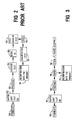
- FIG 1 shows the bathtub reliability curve.
- Burn-in curve 30 approaches the normal life failure rate 30 much faster than components which have received no burn-in on curve 20. In this way, manufacturer's warrant periods can be shortened and projected warranty costs can be estimated more accurately over the shorter warranty period. With burn-in, most of the failures can be induced by burn-in during the period the product is still with the manufacturer.
- the point 60 is the time it takes to find all of the infant mortalities without burn-in.
- the point 50 marks approximately the time period, within one time constant, it takes to find all of the infant mortalities. It is generally expensive and usually impractical to exercise a component or product for the length of time it would take to find all of the infant mortalities before sending the product to the customer.
- the length of time required to exercise the component or product in order to find all of the infant mortalities is reduced and can be reduced to such an extent that it is feasible and practical to burn-in the product and find most if not all infant mortalities.
- the time period to come within one time constant of finding all of the infant mortalities varies.
- Prior burn-in procedures have taken from 1000 hours to several hundred hours.
- Bambi (80) takes from about 1 hour to 20 hours depending the number of components to be tested, implementation, test coverage, and the product environment being tested for. Bambi significantly reduces the time required to find substantially all of the infant failures.
- Figure 2 shows the prior art process sequence.
- the component is fabricated at step 100.
- all of the components are tested and sorted into functional and non-functional components to avoid the expense of packaging non-functional components.
- Typical yields can be 10- to 901 depending on the size and complexity of the component.
- the functional components are sent on to packaging 103.
- package 103 the components are subjected to a package test to sort out good components from bad components.
- package test includes tests which could not have been done accurately at wafer sort die test 102.
- Typical package test yields are 901 to 1001.
- After package test 104, a burn-in is done to induce infant mortalities; functional parts that will soon fail because of an inherent weakness in its fabrication not normally found.
- This burn-in has been a batch processing, sometimes hundreds of parts are put into an environmentally controlled chamber. As discussed in the background, the burn-in can also be monitored and a test during burn-in can also be incorporated. After burn-in 106, even if monitored or a test during burn-in incorporated, typically a post burn-in test 108 is done. After post burn-in test 108, the components are put into stock, shipped to the product manufacturer, or directly assembled into the product.
- a component qualification test 112 is done just before the component is assembled into the product.
- the reason for a qualification test is to further improve the reliability of the component for the particular product it will go into. This may be because the product has peculiar stress and component requirements for which it has not been previously tested or screened. It may be because the product manufacturer wants better reliability than what the component manufacturer can deliver and it is worth it to the product manufacturer to make further tests.
- Stress testing can be done at the qualification test 112. Typically this has also been a batch test with a single component at a time post qualification burn-in test. However, a one step gualification test doing one component at a time has been developed and used in the prior art. This method is for D.C. parametric and D.C. functional testing electronic components using an HP 5045 tester for post burn-in test to reduce infant mortality rates and provide for a cost effective timely procedure to sort out bad components and pass good components.
- the test comprises the steps of: 1) establishing a go/no go criteria using empirically derived test limits established by trial and error from characterizing a particular group of components which fall within pass limits at normal operating temperature; 2) stabilizing the component at a temperature below test operating temperature; 3) placing component in a test means having a test site heater for testing component; 4) heating the component package by an airflow and by the test site heater at a rate of 100 to 300 degree centigrade per minute; 5) heating the component by performing multiple tests using normal operating voltages and applying normal operating bias voltages to the component; 6) multiple testing of the component until the package is within a predetermined thermal time constant of the internal die at the test operating temperature; 7) determining whether component is a good component using the go/no go criteria; 8) sorting the component so that a good component goes into a pass sort group and a bad component goes into a fail sort group.
- This process combined the single-component-at-a-time used at the package test with the stress conditions used at the burn-in step.
- This test was limited because it only provided a gross screen for D.C. parameter and D.C. functionals and sorting was done with respect to historical data of ostensibly good parts and not relative to the individual component value and its projected value under stress conditions. This sort would pass bad parts (Type II error) for at least these reasons, the components were not tested for A.C. parameter and A.C.
- the components were not tested at high frequency, the components were not subjected to a voltage stress in combination with the environmental stress of temperature and humidity, temperature cycle/shock, and the component stress values were not compared to the initial values of the component, but only compared to an historical range derived from values obtained from previous testing.
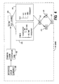
- Figure 3 shows one implementation of the invention which allows the consolidation of package test 104, burn-in 106, post burn-in test 108, and product manufacturer qualification test 112.
- This process uses the Schlumberger Sentry-15 tester to perform A.C. parameter and A.C. functional test, D.C. parameter and D.C. functional test, voltage stress, and high frequency test. Any equivalent tester could be used, for example, the HP 82000, Teradyne, or Megatest. All the tests can be performed while various stresses of temperature and voltage are superimposed.
- Bambi is a single component at a time process.
- Bambi is a serial test for one component, but multiple Bambi processes can be done with multiple components in parallel. Since Bambi is not a batch process, it can be automated. This reduces handling and reduces failures induced by handling and manual processing.
- Bambi can also be implemented at the wafer level test called wafer sort test die 102.
- wafer sort test die 102 At the wafer level, the die is not yet packaged and is still in wafer form. Typically, there are hundreds to thousands of identical die on each wafer. The number of die per wafer depends on the size of the wafer and the size of the individual die. The wafer level tester would test each die using the Bambi method. This allows the rejection of low reliability die before the expense of packaging the die is incurred. The costs of assembly and packaging the die can be 50-751 of the cost of the component.
- a burn-in method which can be implemented at the wafer level, before packaging, can provide significant savings depending on the reliability required for the component and the proportion of reliability failures that would be packaged if not found at the wafer level.
- Figure 4 shows each step in an embodiment of the test method.
- the integrated circuit component 400 is loaded into an IC handler/loader 402 designed to heat the component to just below the final test temperature and queue the component into the test site.
- the IC handler/loader loads the component into the test chamber 406.
- the component is repeatedly tested 410 for D.C. parameter and D.C. functionals, A.C. parameter and A.C. functionals, and high frequency, during which stresses are applied 408. Stresses are applied 408; the temperature is being ramped up, generally between 100 to 300 degrees centigrade per minute, and voltage and high frequency step stresses are periodically introduced. Sorting 412 can take place even during the test/stress process.
- the resulting test values are correlated with respect to the stress being experienced by the component. These are compared to expected values calculated as a function of the initial values of the test and the value of the stress being experienced by the component. This comparison can be done with intermediate test values while the test/stress is generating subsequent values. In fact, the comparison may result in a sort fail 416 before a complete test is done if an intermediate value fails the comparison. After testing, the component exits 418 the test chamber and is separated into pass and fail bins depending on the compo,'ent performance during the testing and comparison to expected values.
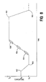
- Figure 5 compares the temperature rise of the die 500 to the package 502 when both parts of the component start at the same temperature, the temperature soak 450 at the loader/handler 402.
- the die 500 heats up faster than the package because of the multiple electrical tests and stresses being directly imposed upon the die.
- the package heats up from the air flow heat of the test system and by conduction from the die 500.
- equilibrium 504 is reached when the die and package are at the same temperature.
- the multiple test/stress continues until the equilibrium 504 or until the temperature of the package is within a predetermined thermal time constant 506 from the equilibrium point 504.
- the temperature rise that is, the slope of 500 during the test, is 100 to 300 degrees centigrade per minute.
- Figure 6 is a specific example how a comparison between measured values and expected values is done.
- Two sorting schemes are shown: go/no go limits are shown by the range 600 to 610 and the relative comparison scheme is shown by 602 and 604.
- Thecurve 600,610 is generated by historical data of known good parts.
- the curves 602 and 604 are generated from the points P0 and C0 respectively and a model of the stress being applied and the parameter being measured.
- This example shows two sets of potential parameter values, set P and set C.
- Set P shows what can happen as one stress condition, temperature, changes during the test.
- a first test is done and an initial parameter value P0 is obtained. From P0, a mathematical surface is generated as a function of the stress involved and the relationship to the test P.
- Test C shows that a fail can occur at any time during the stress conditions. With BAMBI sorting technique, it is not necessary to wait until a value is obtained which is outside of the specification limits 600, 610. If C2 is obtained, even though it is within the specification limits the component presents a reliability risk since C2 lies outside of the mathematical curve 604 generated by C0. The test can end at the intermediate value C2. No further measurements at T3 and T4 need to be taken.
- FIG. 7 shows another implementation of Bambi.
- Bambi could be put into an incoming quality assurance (QA).
- QA quality assurance
- the components are processed through Bambi.
- the components are split up and only a sample from the lot are put through either a Highly Accelerated Stress Test (HAST) 702 or a Temperature Cycle (TC) 704 for twenty hours.
- the HAST test is a moisture resistance test, performed at various humidities and temperatures while the component is under static bias. Another way of viewing HAST is to consider it an accelerated 85/85 (85 degrees centigrade at 851 relative humidity) moisture resistance test.
- TC is cycling the component between two temperature extremes (generally very hot, 150 degrees centigrade and very cold, minus 55 degrees centigrade) without the component under bias, all pins are floating. After this, the components are processed through Bambi 116 again.
- Figure 8 illustrates a version of the Bambi process where the first test temperature 800 is below the normal operating test temperature of the component and below room temperature 802.
- the initial temperature soak 402 before going into the test chamber is a cooling temperature ramp.
- the Bambi process steps 408 through 412 are done.
- Another set of stress/tests 408 through 412 can be done for other periods, 806 and 808.
- This example shows three such periods. Any multiple of periods could be done including having one period which extended over most of the temperature rise. Each period would be a complete stress/test and multiple values could be taken within each period. The sort would take place within a period 804, and not necessarily between two periods 804 and 806.
- Bambi may employ more than one of these temperature cycles.
- the component could be placed into the temperature soak again in order for the component to reach temperature point 800. The component would then be ready to start another series of 804 through 808.
- Loader/handlers/temperature soaks 402 and testers 406 could be aligned in series so multiple cycles could proceed uninterrupted by manual processing. Also, loaders 402 and testers 406 can be aligned in parallel in order to increase capacity.
- Figure 9 shows the benefits of Bambi in detecting oxide defects.
- V1 to V2 oxide defects are accelerated to a greater extent than by using temperature T1 to T2 alone.
- the activation energy in the Arrhenius equation [time- temperature-independent constant*exponential(activation energy/ Boltzmann's constant*absolute temperature)] for oxide defects is small with respect to temperature increases as compared to voltage increases. The combination of temperature, voltage, and high frequency stress even further accelerates infant failures due to oxide defects.
Landscapes
- Physics & Mathematics (AREA)
- General Physics & Mathematics (AREA)
- Testing Of Individual Semiconductor Devices (AREA)
- Tests Of Electronic Circuits (AREA)
Applications Claiming Priority (2)
| Application Number | Priority Date | Filing Date | Title |
|---|---|---|---|
| US07/362,898 US5030905A (en) | 1989-06-06 | 1989-06-06 | Below a minute burn-in |
| US362898 | 1989-06-06 |
Publications (3)
| Publication Number | Publication Date |
|---|---|
| EP0407029A2 true EP0407029A2 (de) | 1991-01-09 |
| EP0407029A3 EP0407029A3 (en) | 1991-09-11 |
| EP0407029B1 EP0407029B1 (de) | 1995-06-28 |
Family
ID=23427956
Family Applications (1)
| Application Number | Title | Priority Date | Filing Date |
|---|---|---|---|
| EP90305830A Expired - Lifetime EP0407029B1 (de) | 1989-06-06 | 1990-05-29 | Verfahren zum Einbrennen in weniger als einer Minute |
Country Status (3)
| Country | Link |
|---|---|
| US (1) | US5030905A (de) |
| EP (1) | EP0407029B1 (de) |
| DE (1) | DE69020442T2 (de) |
Cited By (2)
| Publication number | Priority date | Publication date | Assignee | Title |
|---|---|---|---|---|
| WO1994009378A1 (en) * | 1992-10-13 | 1994-04-28 | Cree Research, Inc. | System and method for accelerated degradation testing of semiconductor devices |
| WO2004038437A1 (en) * | 2002-10-23 | 2004-05-06 | Intel Corporation | Voltage and thermal resistance classification of ics |
Families Citing this family (28)
| Publication number | Priority date | Publication date | Assignee | Title |
|---|---|---|---|---|
| US5646540A (en) * | 1989-04-19 | 1997-07-08 | Interuniversitair Micro-Elektronic Centrum Vzw | Apparatus and method for measuring electromagnetic ageing parameter of a circuit element and predicting its values |
| US5391984A (en) * | 1991-11-01 | 1995-02-21 | Sgs-Thomson Microelectronics, Inc. | Method and apparatus for testing integrated circuit devices |
| US5361032A (en) * | 1992-01-27 | 1994-11-01 | Motorola, Inc. | Method of troubleshooting electronic circuit board assemblies using temperature isolation |
| EP0568294B1 (de) * | 1992-04-27 | 1998-06-24 | Fujitsu Limited | Testverfahren für integrierte Halbleiter-Schaltung |
| US5677853A (en) * | 1994-11-16 | 1997-10-14 | Delco Electronics Corp. | Product testing by statistical profile of test variables |
| US5583875A (en) * | 1994-11-28 | 1996-12-10 | Siemens Rolm Communications Inc. | Automatic parametric self-testing and grading of a hardware system |
| US5570027A (en) * | 1995-04-19 | 1996-10-29 | Photocircuits Corporation | Printed circuit board test apparatus and method |
| US5721496A (en) * | 1996-01-23 | 1998-02-24 | Micron Technology, Inc. | Method and apparatus for leak checking unpackaged semiconductor dice |
| US5742169A (en) * | 1996-02-20 | 1998-04-21 | Micron Technology, Inc. | Apparatus for testing interconnects for semiconductor dice |
| US5744975A (en) * | 1996-06-06 | 1998-04-28 | International Business Machines Corporation | Enhanced defect elimination process for electronic assemblies via application of sequentially combined multiple stress processes |
| US5760595A (en) * | 1996-09-19 | 1998-06-02 | International Business Machines Corporation | High temperature electromigration stress test system, test socket, and use thereof |
| US5954832A (en) * | 1997-03-14 | 1999-09-21 | International Business Machines Corporation | Method and system for performing non-standard insitu burn-in testings |
| US6329831B1 (en) * | 1997-08-08 | 2001-12-11 | Advanced Micro Devices, Inc. | Method and apparatus for reliability testing of integrated circuit structures and devices |
| US6125336A (en) * | 1998-02-03 | 2000-09-26 | Micron Electronics, Inc. | Apparatus for device qualification |
| US6122600A (en) * | 1998-02-03 | 2000-09-19 | Micron Electronics, Inc. | Method device qualification |
| US6326800B1 (en) * | 1999-06-10 | 2001-12-04 | International Business Machines Corporation | Self-adjusting burn-in test |
| US7149673B1 (en) * | 1999-09-09 | 2006-12-12 | Cingular Wireless Ii, Llc | Method for estimating changes in product life for a redesigned product |
| US6598182B1 (en) * | 1999-09-29 | 2003-07-22 | International Business Machines Corporation | Electromigration and extrusion monitor and control system |
| US6445206B1 (en) * | 2000-05-31 | 2002-09-03 | Agere Systems Guardian Corp. | Method and apparatus for determining yield impacting tests at wafer level package level for semiconductor devices |
| US6820029B2 (en) | 2000-12-22 | 2004-11-16 | United Microelectronics Corp. | Method for determining failure rate and selecting best burn-in time |
| DE10115280C2 (de) * | 2001-03-28 | 2003-12-24 | Infineon Technologies Ag | Verfahren zum Klassifizieren von Bauelementen |
| US6980016B2 (en) | 2001-07-02 | 2005-12-27 | Intel Corporation | Integrated circuit burn-in systems |
| US7120566B1 (en) | 2001-07-06 | 2006-10-10 | Cingular Wireless Ii, Llc | Method for estimating changes in product life resulting from HALT using exponential acceleration model |
| US7260509B1 (en) * | 2001-07-06 | 2007-08-21 | Cingular Wireless Ii, Llc | Method for estimating changes in product life resulting from HALT using quadratic acceleration model |
| US7265561B2 (en) * | 2003-09-30 | 2007-09-04 | International Business Machines Corporation | Device burn in utilizing voltage control |
| US7127371B2 (en) * | 2003-10-08 | 2006-10-24 | Ge Medical Systems Information | Customized medical equipment preventative maintenance method and system |
| US9152517B2 (en) | 2011-04-21 | 2015-10-06 | International Business Machines Corporation | Programmable active thermal control |
| US10132860B2 (en) | 2016-10-28 | 2018-11-20 | Nxp Usa, Inc. | Systems and methods for testing package assemblies |
Family Cites Families (10)
| Publication number | Priority date | Publication date | Assignee | Title |
|---|---|---|---|---|
| US3748579A (en) * | 1971-11-12 | 1973-07-24 | Bell Telephone Labor Inc | Method for determining concentration profiles of deep levels on both sides of a p-n junction |
| US3943442A (en) * | 1974-11-11 | 1976-03-09 | Nasa | Method and apparatus for measurement of trap density and energy distribution in dielectric films |
| DE3037192A1 (de) * | 1980-10-02 | 1982-05-06 | Licentia Gmbh | Testverfahren fuer halbleiteranordnungen |
| US4420722A (en) * | 1980-11-14 | 1983-12-13 | Rca Corporation | Testing semiconductor furnaces for heavy metal contamination |
| US4483629A (en) * | 1983-01-05 | 1984-11-20 | Syracuse University | Dynamic testing of electrical conductors |
| USRE32625E (en) * | 1983-01-05 | 1988-03-15 | Syracuse University | Dynamic testing of electrical conductors |
| JPS6168569A (ja) * | 1984-09-10 | 1986-04-08 | インタ−ナショナル ビジネス マシ−ンズ コ−ポレ−ション | 電子装置を鑑別するための最大温度の決定方法 |
| US4739258A (en) * | 1986-07-11 | 1988-04-19 | Syracuse University | Dynamic testing of thin-film conductor |
| IT1201837B (it) * | 1986-07-22 | 1989-02-02 | Sgs Microelettronica Spa | Sistema per la verifica della funzionalita' e delle caratteristiche di dispositivi a semiconduttore di tipo eprom durante il "burn-in" |
| US4855672A (en) * | 1987-05-18 | 1989-08-08 | Shreeve Robert W | Method and process for testing the reliability of integrated circuit (IC) chips and novel IC circuitry for accomplishing same |
-
1989
- 1989-06-06 US US07/362,898 patent/US5030905A/en not_active Expired - Lifetime
-
1990
- 1990-05-29 EP EP90305830A patent/EP0407029B1/de not_active Expired - Lifetime
- 1990-05-29 DE DE69020442T patent/DE69020442T2/de not_active Expired - Fee Related
Cited By (6)
| Publication number | Priority date | Publication date | Assignee | Title |
|---|---|---|---|---|
| WO1994009378A1 (en) * | 1992-10-13 | 1994-04-28 | Cree Research, Inc. | System and method for accelerated degradation testing of semiconductor devices |
| US5381103A (en) * | 1992-10-13 | 1995-01-10 | Cree Research, Inc. | System and method for accelerated degradation testing of semiconductor devices |
| WO2004038437A1 (en) * | 2002-10-23 | 2004-05-06 | Intel Corporation | Voltage and thermal resistance classification of ics |
| US7109737B2 (en) | 2002-10-23 | 2006-09-19 | Intel Corporation | Arrangements having IC voltage and thermal resistance designated on a per IC basis |
| US7112979B2 (en) | 2002-10-23 | 2006-09-26 | Intel Corporation | Testing arrangement to distribute integrated circuits |
| US7233162B2 (en) | 2002-10-23 | 2007-06-19 | Intel Corporation | Arrangements having IC voltage and thermal resistance designated on a per IC basis |
Also Published As
| Publication number | Publication date |
|---|---|
| DE69020442T2 (de) | 1995-11-16 |
| EP0407029B1 (de) | 1995-06-28 |
| US5030905A (en) | 1991-07-09 |
| EP0407029A3 (en) | 1991-09-11 |
| DE69020442D1 (de) | 1995-08-03 |
Similar Documents
| Publication | Publication Date | Title |
|---|---|---|
| US5030905A (en) | Below a minute burn-in | |
| JP7105977B2 (ja) | 検査システム、ならびに検査システムの故障解析・予知方法 | |
| US7710137B2 (en) | Method and apparatus for relative testing of integrated circuit devices | |
| US5589765A (en) | Method for final testing of semiconductor devices | |
| US6175812B1 (en) | Method and system for dynamic duration burn-in | |
| KR100429116B1 (ko) | 반도체 ic 소자의 검사 공정 손실 요인 자동 분석 및관리 시스템과 그 방법 | |
| US6429677B1 (en) | Method and apparatus for characterization of gate dielectrics | |
| CN115146968A (zh) | 一种卫星用裸芯片质量评价的方法 | |
| US8928346B2 (en) | Method for an improved checking of repeatability and reproducibility of a measuring chain for semiconductor device testing | |
| US7983778B2 (en) | Method and apparatus for reducing setups during test, mark and pack operations | |
| US7617427B2 (en) | Method and apparatus for detecting defects in integrated circuit die from stimulation of statistical outlier signatures | |
| US6230293B1 (en) | Method for quality and reliability assurance testing of integrated circuits using differential Iddq screening in lieu of burn-in | |
| US6101458A (en) | Automatic ranging apparatus and method for precise integrated circuit current measurements | |
| Gralian | Next generation burn-in development | |
| Lee et al. | IC handler throughput evaluation for test process optimization | |
| JP2002156404A (ja) | 半導体測定方法及び半導体測定装置 | |
| Bordogna et al. | New R&R Methodology in Semiconductor Manufacturing Electrical Testing | |
| Titu-Marius | Environmental Stress Screening and Burn-in. | |
| Băjenescu | Environmental Stress Screening and Burn-in | |
| JP2002131372A (ja) | 半導体デバイスの検査方法及び検査装置 | |
| Appello et al. | An innovative and low-cost industrial flow for reliability characterization of SoCs | |
| Titu-Marius | Environmental Stress Screening (ESS) and Burn-in | |
| JP2001074808A (ja) | 電子部品試験装置および電子部品の試験方法 | |
| Beck | Practical application of statistical process control in semiconductor manufacturing | |
| Kuokka | Use of stress screening in electrical system production quality control |
Legal Events
| Date | Code | Title | Description |
|---|---|---|---|
| PUAI | Public reference made under article 153(3) epc to a published international application that has entered the european phase |
Free format text: ORIGINAL CODE: 0009012 |
|
| AK | Designated contracting states |
Kind code of ref document: A2 Designated state(s): DE FR GB |
|
| PUAL | Search report despatched |
Free format text: ORIGINAL CODE: 0009013 |
|
| AK | Designated contracting states |
Kind code of ref document: A3 Designated state(s): DE FR GB |
|
| 17P | Request for examination filed |
Effective date: 19911127 |
|
| 17Q | First examination report despatched |
Effective date: 19921207 |
|
| GRAA | (expected) grant |
Free format text: ORIGINAL CODE: 0009210 |
|
| AK | Designated contracting states |
Kind code of ref document: B1 Designated state(s): DE FR GB |
|
| REF | Corresponds to: |
Ref document number: 69020442 Country of ref document: DE Date of ref document: 19950803 |
|
| ET | Fr: translation filed | ||
| PLBE | No opposition filed within time limit |
Free format text: ORIGINAL CODE: 0009261 |
|
| STAA | Information on the status of an ep patent application or granted ep patent |
Free format text: STATUS: NO OPPOSITION FILED WITHIN TIME LIMIT |
|
| 26N | No opposition filed | ||
| REG | Reference to a national code |
Ref country code: GB Ref legal event code: 732E |
|
| REG | Reference to a national code |
Ref country code: FR Ref legal event code: TP |
|
| REG | Reference to a national code |
Ref country code: GB Ref legal event code: IF02 |
|
| PGFP | Annual fee paid to national office [announced via postgrant information from national office to epo] |
Ref country code: DE Payment date: 20070702 Year of fee payment: 18 |
|
| PGFP | Annual fee paid to national office [announced via postgrant information from national office to epo] |
Ref country code: GB Payment date: 20070525 Year of fee payment: 18 |
|
| PGFP | Annual fee paid to national office [announced via postgrant information from national office to epo] |
Ref country code: FR Payment date: 20070517 Year of fee payment: 18 |
|
| GBPC | Gb: european patent ceased through non-payment of renewal fee |
Effective date: 20080529 |
|
| REG | Reference to a national code |
Ref country code: FR Ref legal event code: ST Effective date: 20090119 |
|
| PG25 | Lapsed in a contracting state [announced via postgrant information from national office to epo] |
Ref country code: DE Free format text: LAPSE BECAUSE OF NON-PAYMENT OF DUE FEES Effective date: 20081202 Ref country code: FR Free format text: LAPSE BECAUSE OF NON-PAYMENT OF DUE FEES Effective date: 20080602 |
|
| PG25 | Lapsed in a contracting state [announced via postgrant information from national office to epo] |
Ref country code: GB Free format text: LAPSE BECAUSE OF NON-PAYMENT OF DUE FEES Effective date: 20080529 |