EP0405553B1 - Optisches Zeitbereichsreflektometer mit einem optischen Element, das drei Steuerarten für Schwingung, Dämpfung und Verstärkung enthält - Google Patents
Optisches Zeitbereichsreflektometer mit einem optischen Element, das drei Steuerarten für Schwingung, Dämpfung und Verstärkung enthält Download PDFInfo
- Publication number
- EP0405553B1 EP0405553B1 EP90112358A EP90112358A EP0405553B1 EP 0405553 B1 EP0405553 B1 EP 0405553B1 EP 90112358 A EP90112358 A EP 90112358A EP 90112358 A EP90112358 A EP 90112358A EP 0405553 B1 EP0405553 B1 EP 0405553B1
- Authority
- EP
- European Patent Office
- Prior art keywords
- light
- laser
- optical
- optical fiber
- mode
- Prior art date
- Legal status (The legal status is an assumption and is not a legal conclusion. Google has not performed a legal analysis and makes no representation as to the accuracy of the status listed.)
- Expired - Lifetime
Links
- 230000003287 optical effect Effects 0.000 title claims description 39
- 230000010355 oscillation Effects 0.000 title claims description 22
- 230000003321 amplification Effects 0.000 title claims description 18
- 238000003199 nucleic acid amplification method Methods 0.000 title claims description 18
- 239000013307 optical fiber Substances 0.000 claims description 31
- 239000004065 semiconductor Substances 0.000 claims description 18
- 238000002310 reflectometry Methods 0.000 claims description 9
- 230000002238 attenuated effect Effects 0.000 claims description 4
- 230000005284 excitation Effects 0.000 description 15
- 239000000835 fiber Substances 0.000 description 12
- 229910052761 rare earth metal Inorganic materials 0.000 description 11
- 230000005540 biological transmission Effects 0.000 description 10
- 150000002910 rare earth metals Chemical class 0.000 description 9
- 230000006870 function Effects 0.000 description 8
- 238000000034 method Methods 0.000 description 8
- 238000010586 diagram Methods 0.000 description 4
- 230000010287 polarization Effects 0.000 description 4
- 229920006395 saturated elastomer Polymers 0.000 description 4
- 230000008569 process Effects 0.000 description 3
- 230000004044 response Effects 0.000 description 3
- 230000002269 spontaneous effect Effects 0.000 description 3
- 230000007704 transition Effects 0.000 description 3
- 229910052691 Erbium Inorganic materials 0.000 description 2
- 238000001069 Raman spectroscopy Methods 0.000 description 2
- UYAHIZSMUZPPFV-UHFFFAOYSA-N erbium Chemical compound [Er] UYAHIZSMUZPPFV-UHFFFAOYSA-N 0.000 description 2
- 239000003921 oil Substances 0.000 description 2
- 238000010521 absorption reaction Methods 0.000 description 1
- 230000004913 activation Effects 0.000 description 1
- 230000001427 coherent effect Effects 0.000 description 1
- 239000012141 concentrate Substances 0.000 description 1
- 238000002347 injection Methods 0.000 description 1
- 239000007924 injection Substances 0.000 description 1
- 230000007935 neutral effect Effects 0.000 description 1
- 230000002093 peripheral effect Effects 0.000 description 1
- 238000009738 saturating Methods 0.000 description 1
- 239000000243 solution Substances 0.000 description 1
- 230000003595 spectral effect Effects 0.000 description 1
- 239000000758 substrate Substances 0.000 description 1
Images




Classifications
-
- G—PHYSICS
- G01—MEASURING; TESTING
- G01M—TESTING STATIC OR DYNAMIC BALANCE OF MACHINES OR STRUCTURES; TESTING OF STRUCTURES OR APPARATUS, NOT OTHERWISE PROVIDED FOR
- G01M11/00—Testing of optical apparatus; Testing structures by optical methods not otherwise provided for
- G01M11/30—Testing of optical devices, constituted by fibre optics or optical waveguides
- G01M11/31—Testing of optical devices, constituted by fibre optics or optical waveguides with a light emitter and a light receiver being disposed at the same side of a fibre or waveguide end-face, e.g. reflectometers
- G01M11/3109—Reflectometers detecting the back-scattered light in the time-domain, e.g. OTDR
-
- G—PHYSICS
- G01—MEASURING; TESTING
- G01M—TESTING STATIC OR DYNAMIC BALANCE OF MACHINES OR STRUCTURES; TESTING OF STRUCTURES OR APPARATUS, NOT OTHERWISE PROVIDED FOR
- G01M11/00—Testing of optical apparatus; Testing structures by optical methods not otherwise provided for
- G01M11/30—Testing of optical devices, constituted by fibre optics or optical waveguides
- G01M11/31—Testing of optical devices, constituted by fibre optics or optical waveguides with a light emitter and a light receiver being disposed at the same side of a fibre or waveguide end-face, e.g. reflectometers
- G01M11/319—Reflectometers using stimulated back-scatter, e.g. Raman or fibre amplifiers
Definitions
- the present invention relates generally to an optical time domain reflectometer (hereinafter, referred to as "OTDR"), and more particularly to an OTDR using an optical element with three control modes of oscillation, attenuation and amplification.
- OTDR optical time domain reflectometer
- this invention relates to an OTDR for measuring transmission characteristics of an optical fiber and, for example, identifying the location of a fault in an optical fiber transmission path.
- an optical element when a test light pulse is generated, an optical element is used as a light source.
- the optical element When a pulse reflected from an optical fiber is received, the optical element is used as a light amplifier or a light attenuator.
- saturation of a light receiver due to Fresnel reflection can be prevented, and Rayleigh scattering light can be measured.
- an acoustic/optical element with small loss is provided between an light source, an optical fiber, and a receiver, thereby changing the light path.
- This A/O element is expensive, and optical alignment between a transmission path and a reception path is difficult.
- U. S. Patent No. 4,070,118 discloses an OTDR wherein an optical element (e.g. laser) is employed as an oscillator or an amplifier, without providing an A/O element.
- an optical element e.g. laser
- This OTDR will now be described with reference to Fig. 1.
- a laser 61 When a laser 61 is supplied with a current pulse, exceeding an oscillation limit value, it generates a test pulse.
- the test pulse 65 is applied to a light transmission body 62.
- a light pulse 66 is generated from the laser 61 and is applied to a light receiver 64 thereby marking a zero point on a time scale.
- the laser 61 lowers its operation current slightly below the oscillation limit value, in order to perform an amplification function.
- a reflected pulse 67 reflected from a fault point of the light transmission body 62 is optically amplified by the laser 61 when it passes through the laser 61.
- the amplified pulse 67 is applied to the light receiver 64.
- the light pulses 66 and 67 input to the light receiver 64 are converted to electric signals, and the electric signals reach outputs A.
- the signals output from the light receiver 64 are observed by an oscilloscope (not shown in Fig. 1) or are recorded on a recording device.
- the conventional OTDR shown in Fig. 1 has the problem, as is explained by referring to Fig. 2.
- the conventional OTDR shown in Fig. 1 is designed mainly to measure Fresnel reflection light, and is not designed to measure Rayleigh scattering light.
- this conventional OTDR is employed to measure both Fresnel reflection light and Rayleigh scattering light, the Rayleigh scattering light (indicated by a broken line D in Fig. 2) is masked (as shown by a solid line C in Fig. 2) and cannot be measured.
- the laser 61 and the light transmission body 62 are coupled by a connector (not shown).
- the reflected light passing through the laser 61 includes a Fresnel's reflection light component (denoted by B in Fig. 2), a Fresnel's reflection light component (denoted by C in Fig. 2) and a Rayleigh scattering light component occurring at the fault point 63.
- the Fresnel's reflection light has a high power and is amplified through the laser 61, thus saturating the light receiver 64. Once the light receiver 64 is saturated, it takes a considerable amount of time for the light receiver 64 to be restored to the normal state. Consequently, the OTDR shown in Fig. 1 fails to observe a peculiar point existing just after the connector or the fault point 63 (e.g. component D in Fig. 2, or a slight loss due to a welded point for connection of an extended light transmission body).
- an object of the present invention to provide a new and improved optical time domain reflectometer with three control modes of oscillation, attenuation and amplification for an optical element.
- This optical time domain reflector can prevent the saturation of a light-receiver due to Fresnel's reflection This object is met by an optical time domain reflector according to claim 1.
- an optical time domain reflectometer (OTDR) of the present invention comprises a laser, which may function as a light source (third mode) at the time of generating light pulses and may function as a light amplifier (second mode) or a light attenuator (first mode) at the time of receiving reflected light travelling through an optical fiber, and a control unit for setting the optical element to a desired one of the three modes.
- a laser which may function as a light source (third mode) at the time of generating light pulses and may function as a light amplifier (second mode) or a light attenuator (first mode) at the time of receiving reflected light travelling through an optical fiber, and a control unit for setting the optical element to a desired one of the three modes.
- the optical element which may function as a light source at the time of generating test light pulses and may function as a light amplifier or a light attenuator at the time of receiving reflected light travelling through an optical fiber to be tested.
- Figs. 3A and 3B are a transverse cross-sectional view and a longitudinal cross-sectional view of a so-called SLA semiconductor laser.
- Figs. 4A to 4D illustrate the transition process in a semiconductor.
- Fig. 5 shows an excitation current versus light gain characteristic of the SLA.
- the SLA shown in Figs. 3A and 3B is constituted such that first, second and third n-InP layers are successively formed on an n-InP substrate, an InGaAsP (active layer) is formed in the first to third n-InP layers, and finally a P-InGaAsP electrode is formed.
- the excited electrons return to the original valence band, and excessive energy is emitted as light (Fig. 4C). This state is called a spontaneous emission.
- Fig. 4C This state is called a spontaneous emission.
- Fig. 4D In the state of the inverted distribution, when light having energy greater than Eg is input from the outside, light in phase with the input light is emitted and the electrons fall to the valence band (Fig. 4D). This phenomenon is called stimulated emission.
- the SLA amplifies light.
- the stimulated emission light has a coherent amplification characteris tic in relation to the input light.
- R1 and R2 are input and output facet reflectivities, respectively
- ⁇ is the frequency of input light
- ⁇ ⁇ is the free spectral range (FSR) of the SLA
- ⁇ o is the Fabry-Perot resonance frequency.
- the SLA takes the three modes (regions) of attenuation, amplification and oscillation, in accordance with the injected current. Referring to the characteristic diagram of Fig. 5, the three modes will now be described, with the above equations being employed.
- Fig. 6 is a block diagram showing a first embodiment of the present invention
- Fig. 7 is a timing chart relating to the first embodiment.
- the semiconductor laser functions as a light source, a light amplifier, or a light attenuator in the above-described SLA.
- the mode of operation of the SLA 11 depends on the intensity of the current applied to a current input terminal.
- a first light terminal of the SLA 11 is connected to an optical connector 19, and a second light terminal thereof is connected to a light-receiver 12.
- the light-receiver 11 converts a light signal from the SLA 11 to an electric signal, and sends the electric signal to a signal processor 13.
- the signal processor 13 includes an amplifier, an A/D converter, a memory unit, etc.
- the signal processor 12 processes a signal from the light-receiver 12 and sends the processed signal to a display 15.
- a controller 16 includes a CPU and its peripheral circuit and functions to generate control signals a and b .
- the controller 16 outputs a control signal c .
- the control signals generated from the controller 16 are input to a current generator 15.
- the current generator 15 Based on the control signals from the controller 16, the current generator 15 generates a current which enables the SLA 11 to operate in a desired mode.
- the output from the current generator 15 is applied to the optical element 11.
- the optical connector 19 is coupled to an optical fiber 21.
- Numeral 22 denotes a broken point or the like (including a welded point for connection of an extended fiber, a line connection point using a connector, etc.).
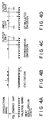
- the current generator 15 When the current generator 15 receives the control signal a from the controller 16, it generates a current I0 and sets the SLA 11 in the oscillation mode (third mode). Namely, the SLA 11 generates light pulses and applies them to the optical fiber 21 and the light-receiver 12. In this case, the output from the light-receiver 12 has a displayed waveform A, as shown in Fig. 7.
- the current generator 15 When the current generator 15 receives the control signal b from the controller 16, it generates a current I L thereby setting the SLA 11 in the attenuation mode (second mode). When Fresnel's reflection light from the optical connector 19 passes through the SLA 11, the reflection light is attenuated by the light-receiver 12, as is indicated by a displayed waveform B in Fig. 7. Subsequently, the current generator 15 generates a current I A which enables the optical element 11 to operate in the amplification mode.
- the controller 16 generates the control signal c in response to the command applied to its terminal 18.
- the control signal c may be generated at a given time point on a time-base axis. If necessary, a plurality of control signals c may be generated.
- the current generator 15 Upon receiving the control signal c , the current generator 15 generates the current I L which enables the SLA 11 to operate in the attenuation mode.
- the SLA 11 attenuates the reflection light thereby preventing the saturation of the light-receiver 12.
- the output from the light-receiver 12 is as is shown by a displayed waveform C in Fig. 7.
- a peculiar point existing just after the broken point 22 of the optical fiber 21 can be exactly observed, as is shown by a displayed waveform D in Fig. 7.
- the signal processor 13 in fact, comprises a first amplifier, a second amplifier, a variable-resistance attenuator, an A/D converter, a data processing unit, a memory unit, an operating unit, etc.
- the oscillation output is applied also to the light-receiver 12, and the light-receiver 12 may be saturated.
- One technique of solving this problem is that the reflectivity R1 of that end portion of the SLA, which faces the light-receiver 12, is made higher than the reflectivity R2 of that end portion of the SLA, which faces the tested optical fiber.
- This technique enables that a light output from a facet of SLA near the light-receiver side is suppressed lower than a light output from a facet of SLA near the fiver-side.
- this technique is disclosed in the Technical Report (OQE82-125, pp. 51-57) of the Institute of Electronics, Information and Communications Engineering.
- a two-part SLA may be used as the optical element 20.
- the controller 16 applies a current Ip higher than an oscillation threshold to an electrode B of the SLA which is closer to the tested optical fiber and enables the electrode B to oscillate.
- a current Is is not applied from the controller 16 to an electrode A of the SLA closer to the light-receiver 12; therefore, light output to the light-receiving element employed in the light-receiver is absorbed, and the light-receiving element is not saturated.
- Fig. 9 is a timing chart of currents Ip and Is generated in the second embodiment shown in Fig. 8.
- a light path disconnecting unit such as an acousto-optical deflector may be provided between the optical element 11 and the light-receiver 12, thereby to shut off the light pass in response to the control signal a .
- Fig. 10 shows an example of the structure of the controller 16 and the current generator 15 employed in the above embodiments.
- a memory 161 stores a control program and a control pattern.
- the control pattern corresponds, for example, the control signals shown in Fig. 6.
- a control signal output from the memory 161 is input to a CPU 162, and is converted to a command in the CPU 162.
- the CPU 162 may be a general-purpose microprocessor.
- the command output from the CPU 162 is applied to a D/A converter 151 through a bus 163 and is converted to an analog signal.
- the D/A converter 151 may be constituted, for example, by an RTI-602 D/A converter board (manufactured by ANALOG DEVICES). Since the resultant analog signal is a voltage signal, it is applied to an V/I converter and is converted to a current signal.
- the V/I converter 152 is constituted, for example, by a V/I converter 0A08 (manufactured by ANALOG DEVICES).
- a maximum output current of the V/I converter 0A08 is 20 mA, and it is insufficient to directly control a light amplifier.
- a driver 153 must be provided.
- the driver 153 may be a general-purpose middle/large power transistor.
- the structure of the controller 16 and the current generator 15 is not limited to this example.
- the gain at the saturation point can be automatically reduced, and the operator's work load is greatly reduced.
- the laser is not limited to the SLA, and it may be replaced with other types of light amplifier, for example, a fiber Raman amplifier or a rare-earth doped fiber laser amplifier as disclosed in the Technical Report (OQE89-18, pp. 55-60) of the Institute of Electronics, Information and Communications Engineering.
- the aforementioned excitation current is replaced with excitation light.
- the light amplifiers, including the SLA may be of the travelling wave type (the reflectivities of both facets of the amplifier are low) or of the resonance type (the reflectivities are high).
- optical fiber type light amplifier (30) is employed as the optical element 30.
- fiber type light amplifiers are classified into the Raman type, the Brillouin type, the rare-earth doped type, etc.
- any one of the fiber type light amplifiers can be used.
- a rare-earth doped optical fiber type light amplifier is employed, for example, in the description that follows. Referring to Fig. 11, there is shown a rare-earth doped optical fiber type light amplifier 30.
- the light amplifier 30 comprises a dichroic beamsplitter 31, an excitation light source 32 connected to a port 2 of the dichroic beamsplitter 31, a rare-earth doped optical fiber 33 connected to a port 3 of the dichroic beamsplitter 31, and a light filter 34 connected to the fiber 33.
- the dichroic beamsplitter 31 has a wavelength selection function.
- the path between the ports 1 and 3 has a low loss property with respect to the desired wavelength for amplification, and the path between the ports 2 and 3 has a low loss property with respect to the excitation wavelength.
- a rare-earth element to be added to the rare-earth doped optical fiber 33 is determined in accordance with the wavelength for amplification.
- erbium (Er) is doped.
- a semiconductor laser which is easy to handle, is widely used as the excitation source 32.
- the oscillation wavelength of the semiconductor laser is determined by the rare-earth element doped to the optical fiber. In the case of use of erbium, the oscillation wavelength is 1.48 ⁇ m or 0.98 ⁇ m.
- the operation of the third embodiment will now be described.
- the inside of the rare-earth-doped optical fiber has an inverted electron distribution as shown in Fig. 4B.
- the signal light is amplified by virtue of the stimulated emission as shown in Fig. 4D.
- the output from the light amplifier 30 includes, in addition to an amplified light component, an excitation light component and a spontaneous emission light component (see Fig. 4C) emitted from the fiber itself.
- the excitation light component and the spontaneous emission light component are not necessary and are removed by the light filter 34 as noise, as compared to the signal light.
- the 12 shows an excitation light power versus gain characteristic of the light amplifier 30.
- An attenuation region is obtained when the light power is lower than P1
- an amplification region is obtained in a range between P1 to P2
- an oscillation region is obtained when the light power is higher than P2.
- the semiconductor laser is used as the excitation light source 32
- a proportional relationship is found in the current versus light output characteristic of the semiconductor laser, as shown in Fig. 13.
- the current versus gain characteristic of the light amplifier 30 is similar to that shown in Fig. 5. Therefore, the semiconductor laser is easily applicable to the present invention.
- the reflectivities R1 and R2, appearing in equation (2) correspond to the reflectances of both end portions of the rare-earth doped optical fiber serving as an amplification medium.
- the values of the reflectances are determined by the difference in refractive index between the rare-earth doped optical fiber and a conventional optical fiber connected thereto.
- the optical time domain reflectometer comprises a laser functioning as a light source when light pulses are generated, and functioning as a light amplifier or a light attenuator when reflected light from an optical fiber is received, and a controller for controlling the mode of operation of the optical element. While reflected light is received, the optical element is used in the light amplification mode. In this time period, the optical element is operated in the attenuation mode at a desired time just after the generation of a light pulse, in which mode the reflected light from the optical fiber is masked. Thus, Fresnel's reflection light occurring at the fault point of the fiber is attenuated, and a peculiar point existing just after the fault point can be exactly observed.
- the use of the two-part semiconductor laser can prevent the light-receiver from being saturated at the time of light pulse generation.
Landscapes
- Physics & Mathematics (AREA)
- Optics & Photonics (AREA)
- Chemical & Material Sciences (AREA)
- Analytical Chemistry (AREA)
- General Physics & Mathematics (AREA)
- Lasers (AREA)
- Semiconductor Lasers (AREA)
- Testing Of Optical Devices Or Fibers (AREA)
Claims (4)
- Optisches Zeitbereichsreflektometer, das folgendes aufweist:
einen Laser (11), um einen Lichtimpuls an eine zu prüfende Lichtleitfaser (21) abzugeben, wobei der Laser (11) in drei Betriebsarten, umfassend Lichtschwingung, Lichtverstärkung und Lichtdämpfung, in Abhängigkeit von dem Wert eines ihm zugeführten Steuerparameters zu betreiben ist, wobei der Laser (11) einen ersten Lichtanschluß hat, von dem in der Schwingungs-Betriebsart ein Lichtimpuls an die zu prüfende Lichtleitfaser (21) abgegeben wird, und einen zweiten Lichtanschluß hat, durch den von der Lichtleitfaser (21) reflektiertes Licht nach Durchgang durch den Halbleiterlaser (11) geleitet wird;
eine Lichtempfangseinrichtung (12), um das reflektierte Licht von dem zweiten Lichtanschluß zu empfangen und das reflektierte Licht in ein elektrisches Signal umzuwandeln;
eine Signalverarbeitungseinrichtung (13), um das von der Lichtempfangseinrichtung (12) abgegebene elektrische Signal einem vorbestimmten Signalverarbeitungsschritt zu unterwerfen, um die Lichtleitfaser (21) zu prüfen; und
eine Steuereinrichtung (15, 16), um den Steuerparameter zur Steuerung des Lasers (11) abzugeben,
dadurch gekennzeichnet,
daß die Steuereinrichtung (15, 16) ausgebildet ist, um an den Laser (11) einen ersten Wert (IO) des Steuerparameters abzugeben, um zuzulassen, daß der Laser (11) in einem ersten Zeitintervall (A) in der Schwingungs-Betriebsart arbeitet, einen zweiten Wert (IL) des Steuerparameters abzugeben, um zuzulassen, daß der Laser (11) in einem zweiten Zeitintervall (B), das unmittelbar auf die Schwingungs-Betriebsart folgt, in der Dämpfungs-Betriebsart arbeitet, während welcher reflektiertes Licht einschließlich Fresnelsche Reflexion gedämpft wird, und einen dritten Wert (IA) des Steuerparameters abzugeben, um zuzulassen, daß der Laser (11) in einem dritten Zeitintervall (C), das unmittelbar auf die Dämpfungs-Betriebsart folgt, in der Verstärkungs-Betriebsart arbeitet, während welcher Reflexionslicht ohne Fresnelsche Reflexion verstärkt wird. - Optisches Zeitbereichsreflektometer nach Anspruch 1, dadurch gekennzeichnet, daß der Laser einen zweiteiligen Halbleiter-Laser (20) aufweist.
- Optisches Zeitbereichsreflektometer nach Anspruch 1, dadurch gekennzeichnet, daß das Reflektometer ferner eine Befehlseinrichtung (18) aufweist, um an die Steuereinrichtung (15, 16) einen Befehl anzulegen, um den zweiten Wert (IL) des Steuerparameters an den Laser (11) ein zweites Mal abzugeben, wodurch der Halbleiter-Laser (11) zu einem gegebenen Zeitpunkt während des dritten Zeitintervalls (C) in der Dämpfungs-Betriebsart betrieben wird.
- Optisches Zeitbereichsreflektometer nach Anspruch 1, dadurch gekennzeichnet, daß das Reflexionsvermögen desjenigen Bereichs des Halbleiter-Lasers (11), der der Lichtempfangseinrichtung (12) zugewandt ist, höher als das Reflexionsvermögen desjenigen Bereichs des Halbleiter-Lasers (11) ist, der der zu prüfenden Lichtleitfaser (21) zugewandt ist.
Applications Claiming Priority (2)
| Application Number | Priority Date | Filing Date | Title |
|---|---|---|---|
| JP169186/89 | 1989-06-30 | ||
| JP16918689 | 1989-06-30 |
Publications (3)
| Publication Number | Publication Date |
|---|---|
| EP0405553A2 EP0405553A2 (de) | 1991-01-02 |
| EP0405553A3 EP0405553A3 (en) | 1992-10-14 |
| EP0405553B1 true EP0405553B1 (de) | 1995-01-11 |
Family
ID=15881828
Family Applications (1)
| Application Number | Title | Priority Date | Filing Date |
|---|---|---|---|
| EP90112358A Expired - Lifetime EP0405553B1 (de) | 1989-06-30 | 1990-06-28 | Optisches Zeitbereichsreflektometer mit einem optischen Element, das drei Steuerarten für Schwingung, Dämpfung und Verstärkung enthält |
Country Status (4)
| Country | Link |
|---|---|
| US (1) | US5028775A (de) |
| EP (1) | EP0405553B1 (de) |
| JP (1) | JPH0387627A (de) |
| DE (1) | DE69015895T2 (de) |
Families Citing this family (16)
| Publication number | Priority date | Publication date | Assignee | Title |
|---|---|---|---|---|
| WO1991012509A1 (en) * | 1990-02-15 | 1991-08-22 | British Telecommunications Public Limited Company | Optical test apparatus |
| US5013907A (en) * | 1990-03-27 | 1991-05-07 | Tektronix, Inc. | Optical time domain testing instrument |
| JPH04274724A (ja) * | 1991-03-02 | 1992-09-30 | Fujikura Ltd | Otdr装置 |
| US5291267A (en) * | 1992-01-22 | 1994-03-01 | Hewlett-Packard Company | Optical low-coherence reflectometry using optical amplification |
| US5446278A (en) * | 1993-12-23 | 1995-08-29 | The United States Of America As Represented By The United States Department Of Energy | Fiber optic sensor employing successively destroyed coupled points or reflectors for detecting shock wave speed and damage location |
| US5491548A (en) * | 1994-03-18 | 1996-02-13 | Tektronix, Inc. | Optical signal measurement instrument and wide dynamic range optical receiver for use therein |
| US5589933A (en) * | 1994-10-24 | 1996-12-31 | Photon Kinetics, Inc. | Optical fiber test instrument with mechanically positioned attenuator |
| US5566263A (en) * | 1995-03-22 | 1996-10-15 | Minnesota Mining And Manufacturing Company | System for tuning an integrated optical switch element |
| US6724524B1 (en) * | 2000-08-18 | 2004-04-20 | Corning Incorporated | Gain control in Raman amplifiers |
| US6784987B2 (en) * | 2001-01-19 | 2004-08-31 | Dbm Optics, Incorporated | Non-linear ranging to control linear ranging measurement device |
| EP1432149B1 (de) * | 2002-12-16 | 2007-08-08 | Aston Photonic Technologies Ltd. | Optisches Wellenleiter-Gitter Abfragesystem und Sensorsystem |
| EP1632766A1 (de) * | 2004-09-03 | 2006-03-08 | Alcatel | Verfahren zum reflektometrischen Über-prüfen einer optischen Übertragungs-leitung, sowie optische Einrichtung und optische Sende- und Empfangseinrichtung |
| US20080266570A1 (en) * | 2007-04-26 | 2008-10-30 | Sezerman Omur M | Detection and location of breaks in distributed brillouin fiber sensors |
| GB2493959B (en) * | 2011-08-25 | 2015-10-14 | Optasense Holdings Ltd | A fibre optic distributed sensor |
| JP6653617B2 (ja) * | 2016-05-09 | 2020-02-26 | 日本電信電話株式会社 | 光パルス試験装置および光パルス試験方法 |
| CN109682308A (zh) * | 2018-12-21 | 2019-04-26 | 河海大学 | 基于光时域反射的塑料光纤裂缝监测装置及监测方法 |
Family Cites Families (5)
| Publication number | Priority date | Publication date | Assignee | Title |
|---|---|---|---|---|
| DE2457930A1 (de) * | 1974-12-07 | 1976-06-10 | Licentia Gmbh | Verfahren zur fehlerortung bei glasfaserlichtleitern |
| DE2850430A1 (de) * | 1978-11-21 | 1980-05-29 | Siemens Ag | Justieren miteinander zu verbindender enden zweier lichtleitfasern |
| US4243320A (en) * | 1979-03-20 | 1981-01-06 | Northern Telecom Limited | Methods for testing optical fibres |
| JPS6086438A (ja) * | 1983-10-18 | 1985-05-16 | Nippon Telegr & Teleph Corp <Ntt> | 光フアイバの試験方法および装置 |
| IT1179209B (it) * | 1984-06-13 | 1987-09-16 | Bordoni Ugo Fondazione | Metodo per la rivelazione di rotture in un cavo in fibra ottica |
-
1990
- 1990-06-26 US US07/543,971 patent/US5028775A/en not_active Expired - Fee Related
- 1990-06-28 EP EP90112358A patent/EP0405553B1/de not_active Expired - Lifetime
- 1990-06-28 DE DE69015895T patent/DE69015895T2/de not_active Expired - Fee Related
- 1990-06-29 JP JP2169987A patent/JPH0387627A/ja active Pending
Also Published As
| Publication number | Publication date |
|---|---|
| DE69015895D1 (de) | 1995-02-23 |
| EP0405553A2 (de) | 1991-01-02 |
| DE69015895T2 (de) | 1995-09-07 |
| JPH0387627A (ja) | 1991-04-12 |
| EP0405553A3 (en) | 1992-10-14 |
| US5028775A (en) | 1991-07-02 |
Similar Documents
| Publication | Publication Date | Title |
|---|---|---|
| US5028775A (en) | Optical time domain reflectometer using optical element with three control modes of oscillation, attenuation and amplification | |
| Stewart et al. | An investigation of an optical fibre amplifier loop for intra-cavity and ring-down cavity loss measurements | |
| US7719666B2 (en) | Distributed optical fiber sensor | |
| US8693512B2 (en) | Frequency referencing for tunable lasers | |
| EP0348235B1 (de) | Verfahren und Vorrichtung zum Beurteilen einer optischen Faser mit Brillouin Verstärkung | |
| Hall et al. | Femtosecond index nonlinearities in InGaAsP optical amplifiers | |
| JP3203611B2 (ja) | 雑音指数測定方法および装置 | |
| US5340979A (en) | Technique for determining the amplified spontaneous emission noise of an optical circuit in the presence of an optical signal | |
| CA2247293A1 (en) | Distributed sensing apparatus | |
| US6016213A (en) | Method and apparatus for optical amplifier gain and noise figure measurement | |
| EP0586103B1 (de) | Messung eines Parameters eines optischen Verstärkers | |
| US5511086A (en) | Low noise and narrow linewidth external cavity semiconductor laser for coherent frequency and time domain reflectometry | |
| JP2007240351A (ja) | 分布型光ファイバセンサ | |
| Fatome et al. | Measurement of nonlinear and chromatic dispersion parameters of optical fibers using modulation instability | |
| US5894488A (en) | Light source with stabilized broadband and associated optical fiber gyroscope | |
| JP3353243B2 (ja) | 雑音指数測定方法 | |
| US6728025B2 (en) | Semiconductor optical amplifier characteristic evaluation method and apparatus | |
| EP0138623B1 (de) | Verfahren zum Testen von optischen Fasern und Apparat zur Ausführung des Verfahrens | |
| US5014015A (en) | Ultra-short optical pulse source | |
| EP0343610B1 (de) | Verfahren zum Charakterisieren von bistabilen Halbleiterlasern | |
| JPS61102081A (ja) | 半導体レ−ザの周波数安定化方法 | |
| JP3344877B2 (ja) | パルスレーザ装置及びotdr装置 | |
| Griffin et al. | Coherence and noise properties of gain-switched Fabry-Perot semiconductor lasers | |
| JP3232546B2 (ja) | Otdr装置 | |
| Ferrari et al. | Subkilohertz fluctuations and mode hopping in high-power grating-stabilized 980-nm pumps |
Legal Events
| Date | Code | Title | Description |
|---|---|---|---|
| PUAI | Public reference made under article 153(3) epc to a published international application that has entered the european phase |
Free format text: ORIGINAL CODE: 0009012 |
|
| 17P | Request for examination filed |
Effective date: 19900628 |
|
| AK | Designated contracting states |
Kind code of ref document: A2 Designated state(s): DE FR GB |
|
| PUAL | Search report despatched |
Free format text: ORIGINAL CODE: 0009013 |
|
| AK | Designated contracting states |
Kind code of ref document: A3 Designated state(s): DE FR GB |
|
| 17Q | First examination report despatched |
Effective date: 19930728 |
|
| GRAA | (expected) grant |
Free format text: ORIGINAL CODE: 0009210 |
|
| AK | Designated contracting states |
Kind code of ref document: B1 Designated state(s): DE FR GB |
|
| REF | Corresponds to: |
Ref document number: 69015895 Country of ref document: DE Date of ref document: 19950223 |
|
| ET | Fr: translation filed | ||
| PLBE | No opposition filed within time limit |
Free format text: ORIGINAL CODE: 0009261 |
|
| STAA | Information on the status of an ep patent application or granted ep patent |
Free format text: STATUS: NO OPPOSITION FILED WITHIN TIME LIMIT |
|
| 26N | No opposition filed | ||
| PGFP | Annual fee paid to national office [announced via postgrant information from national office to epo] |
Ref country code: FR Payment date: 19961108 Year of fee payment: 8 |
|
| PGFP | Annual fee paid to national office [announced via postgrant information from national office to epo] |
Ref country code: GB Payment date: 19970619 Year of fee payment: 8 |
|
| PGFP | Annual fee paid to national office [announced via postgrant information from national office to epo] |
Ref country code: DE Payment date: 19970729 Year of fee payment: 8 |
|
| PG25 | Lapsed in a contracting state [announced via postgrant information from national office to epo] |
Ref country code: GB Free format text: LAPSE BECAUSE OF NON-PAYMENT OF DUE FEES Effective date: 19980628 |
|
| GBPC | Gb: european patent ceased through non-payment of renewal fee |
Effective date: 19980628 |
|
| PG25 | Lapsed in a contracting state [announced via postgrant information from national office to epo] |
Ref country code: FR Free format text: LAPSE BECAUSE OF NON-PAYMENT OF DUE FEES Effective date: 19990226 |
|
| PG25 | Lapsed in a contracting state [announced via postgrant information from national office to epo] |
Ref country code: DE Free format text: LAPSE BECAUSE OF NON-PAYMENT OF DUE FEES Effective date: 19990401 |
|
| REG | Reference to a national code |
Ref country code: FR Ref legal event code: ST |