EP0404561A2 - Electrophotographic developing apparatus - Google Patents
Electrophotographic developing apparatus Download PDFInfo
- Publication number
- EP0404561A2 EP0404561A2 EP90306778A EP90306778A EP0404561A2 EP 0404561 A2 EP0404561 A2 EP 0404561A2 EP 90306778 A EP90306778 A EP 90306778A EP 90306778 A EP90306778 A EP 90306778A EP 0404561 A2 EP0404561 A2 EP 0404561A2
- Authority
- EP
- European Patent Office
- Prior art keywords
- developing roller
- roller
- developing
- toner particles
- rotation
- Prior art date
- Legal status (The legal status is an assumption and is not a legal conclusion. Google has not performed a legal analysis and makes no representation as to the accuracy of the status listed.)
- Granted
Links
Images


Classifications
-
- G—PHYSICS
- G03—PHOTOGRAPHY; CINEMATOGRAPHY; ANALOGOUS TECHNIQUES USING WAVES OTHER THAN OPTICAL WAVES; ELECTROGRAPHY; HOLOGRAPHY
- G03G—ELECTROGRAPHY; ELECTROPHOTOGRAPHY; MAGNETOGRAPHY
- G03G15/00—Apparatus for electrographic processes using a charge pattern
- G03G15/06—Apparatus for electrographic processes using a charge pattern for developing
- G03G15/065—Arrangements for controlling the potential of the developing electrode
-
- G—PHYSICS
- G03—PHOTOGRAPHY; CINEMATOGRAPHY; ANALOGOUS TECHNIQUES USING WAVES OTHER THAN OPTICAL WAVES; ELECTROGRAPHY; HOLOGRAPHY
- G03G—ELECTROGRAPHY; ELECTROPHOTOGRAPHY; MAGNETOGRAPHY
- G03G15/00—Apparatus for electrographic processes using a charge pattern
- G03G15/06—Apparatus for electrographic processes using a charge pattern for developing
- G03G15/08—Apparatus for electrographic processes using a charge pattern for developing using a solid developer, e.g. powder developer
- G03G15/0806—Apparatus for electrographic processes using a charge pattern for developing using a solid developer, e.g. powder developer on a donor element, e.g. belt, roller
- G03G15/0812—Apparatus for electrographic processes using a charge pattern for developing using a solid developer, e.g. powder developer on a donor element, e.g. belt, roller characterised by the developer regulating means, e.g. structure of doctor blade
-
- G—PHYSICS
- G03—PHOTOGRAPHY; CINEMATOGRAPHY; ANALOGOUS TECHNIQUES USING WAVES OTHER THAN OPTICAL WAVES; ELECTROGRAPHY; HOLOGRAPHY
- G03G—ELECTROGRAPHY; ELECTROPHOTOGRAPHY; MAGNETOGRAPHY
- G03G2215/00—Apparatus for electrophotographic processes
- G03G2215/06—Developing structures, details
- G03G2215/0602—Developer
- G03G2215/0604—Developer solid type
- G03G2215/0614—Developer solid type one-component
-
- G—PHYSICS
- G03—PHOTOGRAPHY; CINEMATOGRAPHY; ANALOGOUS TECHNIQUES USING WAVES OTHER THAN OPTICAL WAVES; ELECTROGRAPHY; HOLOGRAPHY
- G03G—ELECTROGRAPHY; ELECTROPHOTOGRAPHY; MAGNETOGRAPHY
- G03G2215/00—Apparatus for electrophotographic processes
- G03G2215/06—Developing structures, details
- G03G2215/0634—Developing device
- G03G2215/0636—Specific type of dry developer device
Definitions
- the present invention relates to electrophotographic developing apparatus.
- An electrophotographic printer generally carries out the processes of: producing a uniform distribution of electrical charges on a surface of an electrostatic latent image carrying body such as an electrophotographic photoreceptor; forming an electrostatic latent image on the electrically charged surface of the electrophotographic photoreceptor by optically writing an image thereon, using a laser beam scanner, an LED (light emitting diode) array, an LCS (liquid crystal shutter) array or the like; visually developing the electrostatic latent image with a developer, i.e. , toner, which is electrically charged to be electrostatically adhered to the electostatic latent image zone; electrostatically transferring the developed visible image to a paper; and fixing the transferred image on the paper.
- the electrophotographic photoreceptor is formed as a photosensitive drum having a cylindrical conductive substrate and a photoconductive insulating film bonded to a cylindrical surface thereof.
- a two-component developer composed of a toner component (colored fine synthetic resin particles) and a magnetic component (magnetic fine carriers) is widely used, as it enables a stable development of the latent image.
- the toner particles typically have an average diameter of about 10 ⁇ m, and the magnetic fine carriers have a diameter ten times larger than the average diameter of the toner particles.
- a developing device using the two-component developer includes a vessel for holding the two-component developer, wherein the developer is agitated by an agitator provided therein. This agitation causes the toner particles and the magnetic carriers to be subjected to triboelectrification, whereby the toner particles are electrostatically adhered to each of the magnetic carriers.
- the developing device also includes a magnetic roller, provided in the vessel as a developing roller, in such a manner that a portion of the magnetic roller is exposed therefrom and faces the surface of the photosensitive drum.
- the magnetic carriers with the toner particles are magnetically adhered to the surface of the magnetic roller to form a magnetic brush therearound, and by rotating the magnetic roller carrying the magnetic brush, the toner particles are brought to the surface of the photosensitive drum for the development of the electrostatic latent image formed theron.
- the developing device In this developing device, a ratio between the toner and magnetic components of the developer body held in the vessel must fall within a predetermined range, to continuously maintain a stable development process. Accordingly, the developing device is provided with a toner supplier from which a toner component is supplied to the two-component developer held in the vessel, to supplement the toner component as it is consumed during the development process, whereby the component ratio of the two-component developer held by the vessel is kept within the predetermined range.
- This use of a two-component developer is advantageous in that a stable development process is obtained thereby, but the developing device per se has the disadvantages of a cumbersome control of a suitable component ratio of the two-component developer, and an inability to reduce the size of the developing device due to the need to incorporate the toner supplier therein.
- a one-component developer is also known in this field, and a developing device using same does not suffer from the above-mentioned disadvantages of the developing device using the two-component developer, because the one-component developer is composed of only a toner component (colored fine synthetic resin particles).
- Two types of the one-component developer are known; a magnetic type and a non-magnetic type.
- a developing device using the magnetic type one-component developer can be constructed in substantially the same manner as that using the two-component developer. Namely, the magnetic type one-component developer also can be brought to the surface of the photosensitive drum by a rotating magnetic roller as in the developing device using the two-component developer.
- the magnetic type one-component developer is suitable for achromatic color (black) printing, but is not suitable for chromatic color printing. This is because each of the toner particles composing the magnetic type one-component developer includes fine magnetic powders having a dark color. In particular, the chromatic color printing obtained from the magnetic type one-component developer appears dark and dull, due to the fine magnetic powders included therein. Conversely, the non-magnetic type one-component developer is particularly suitable for chromatic color printing because it does not include a substance having a dark color, but the non-magnetic type one-component developer cannot be brought to the surface of the photosensitive drum by the magnetic roller as mentioned above.
- a developing device using the non-magnetic type one-component developer is also known, as disclosed in U.S. Patents No. 3,152,012 and No. 3,754,963, Japanese Examined Patent Publication (Kokoku) No.60-12627, and Japanese Unexamined Patent Publications (Kokai) No. 62-976, No. 62-118372, No. 63- 100482, and No. 63-189876.
- These developing devices include a vessel for holding the non-magnetic type one-component developer, and a conductive elastic roller provided within the vessel as a developing roller in such a manner that a portion of the elastic roller is exposed therefrom and can be pressed against the surface of the photosensitive drum.
- the conductive elastic developing roller may be formed of a conductive silicone rubber material or a conductive polyurethane rubber material or the like.
- the toner particles composing the non-magnetic type one-component developer are frictionally entrained by the surface of the conductive rubber developing roller to form a developer layer therearound, whereby the toner particles can be brought to the surface of the photosensitive drum for the development of the electrostatic latent image formed thereon.
- the development process is carried out in such a manner that, at the area of contact between the photosensitive drum and the conductive rubber developing roller carrying the developer layer, the charged toner particles are electrostatically attracted and adhered to the latent image due to a bias voltage supplied to the conductive solid rubber developing roller.
- the developing device further includes a blade member which is resiliently pressed against the surface of the developing roller, to uniformly regulate a thickness of the developer layer formed therearound so that an even development of the latent image can be carried out.
- the blade member may be also used to electrically charge the toner particles by a triboelectrification therebetween and/or by a charge-injection effect resulting from supply of voltage to the conductive blade member.
- the blade member is formed of a conductor such as a conductive rubber material, aluminum, stainless steel, brass or the like.
- the supply of voltage to the blade member also serves to prevent an electrostatical adhesion of the toner particles to the blade member during the regulation of a thickness of the developer layer formed around the developing roller.
- the developing device may be also provided with a toner-developing roller which is rotated in contact with the developing roller so that remaining toner particles not used for the development of the latent image are mechanically removed from the developing roller, whereby a fresh developer layer can be continuously formed on the surface of the developing roller.
- the developer layer formed of the remaining toner particles not used for the development of the latent image should be once removed from the developing roller because it is subjected to physical and electrical affects during the developing process, and thus prevents a physical and electrical even formation of the developer layer around the developing roller.
- the toner-removing roller can be formed of a conductive porous rubber material, so that the remaining toner particles not used during the development of the latent image can be also electrostatically removed from the developing roller.
- a voltage is supplied to the conductive toner-removing roller so that the charged toner particles are electrostatically attracted from the developing roller to the toner-removing roller, whereby not only the mechanical removal of the remaining toner particles but also the electrostatic removal thereof can be carried out.
- the voltages are supplied to the developing roller, the blade member, and the toner-removing roller, and thus a high electrical current flows at localized contacting zones between the developing roller and the blade member and toner-removing roller, resulting in a fusion of the developing roller at the localized contacting zones due to the generation of Joule heat.
- the surface of the developing roller is damaged, the quality of a developed image (and thus a printed image) is deteriorated.
- the developing device when the developing device is in a non-operative condition, the developer layer formed around the developing roller is left as it is. Accordingly, the toner particles existing between the photosensitive drum and the developing roller may be adhered not only to each other but also to the surface of the photosensitive drum, because the developing roller is resiliently pressed against the photosensitive drum, and thus when the developing device is again operated the quality of a printed image is deteriorated.
- An embodiment of the present invention can provide a developing device using a one-component developer composed of toner particles, which device comprises a vessel for holding the developer, and a developing roller rotatably provided within and supported by the vessel in such a manner that a portion of the developing roller is exposed therefrom.
- the exposed portion of the developing roller is pressed against a surface of an electrostatic latent image carrying body, and the developing roller is formed of a conductive elastic (elastomeric) aerial by which the toner particles are entrained to form a developer layer therearound and are carried to the surface of the electrostatic latent image carrying body for development of an electrostatic latent image formed thereon.
- the developing roller is rotated by a drive motor which is driven by a motor drive circuit.
- a blade member is provided within the vessel and is pressed against the developing roller for regulating a thickness of the developer layer formed therearound.
- a developing bias voltage is supplied from a first power source to the developing roller, and a voltage is supplied from a second power source to the blade member to inject an electric charge to the toner particles of the developer layer and/or to prevent an electrostatic adhesion of the toner particles to the blade member.
- the first and second power sources and the motor drive circuit are controlled in such a manner that the supply of the voltages to the developing roller and the blade member is carried out after the developing roller is rotated by the drive motor.
- the first and second power sources and the motor drive circuit are controlled in such a manner that the supply of the voltage to the blade member is prematurely stopped before the supply of the voltage to the developing roller and the rotation of the developing roller are stopped.
- the developing device may comprise a toner-removing roller rotatably provided within and supported by the vessel in such a manner that it is resiliently pressed against the developing roller, the toner-removing roller being formed of a conductive elastic material and being rotated so that remaining toner particles not used for the development of the latent image are mechanically removed from the developing roller, and a third power source for supplying a voltage to the toner-removing roller to electrostatically remove the remaining toner particles from the developing roller.
- the first, second, and third power sources and the motor drive circuit are controlled in such a manner that the supply of the voltages to the developing roller, blade member, and toner-removing roller is carried out after the developing roller is rotated by the drive motor.
- the first, second, and third power sources and the motor drive circuit are controlled in such a manner that the supply of the voltage to the blade member is prematurely stopped before the supply of the voltages to the developing roller and toner-removing roller and the rotation of the developing roller are stopped.
- the second power source for the blade member may be constituted so that one of first and second voltages is selectively supplied to the blade member, the first voltage having a polarity opposite to that of the second voltage.
- the first voltage is supplied to the blade member to inject an electric charge to the toner particles of the developer layer and/or to prevent an electrostatic adhesion of the toner particles to the blade member during the development of the latent image
- the second voltage is supplied to the blade member to electrostatically remove the toner particles of the developer layer from the developing roller after the development of the latent image is completed.
- the first and second power sources and the motor drive circuit are controlled in such a manner that a change of the supply of the first voltage to the supply of the second voltage is carried out before the supply of the voltage to the developing roller and the rotation of the developing roller are stopped.
- the first and second power sources and the motor drive circuit are controlled in such a manner that a change of the supply of the first voltage to the supply of the second voltage is carried out before the supply of the voltage to the developing roller and the rotation of the developing roller are stopped.
- the developing roller is formed of a conductive open-cell foam material so that pore openings are formed over a surface of the developing roller, the pore openings having a diameter which is at most twice an average diameter of the toner particles.
- the conductive open-cell foam material of the developing roller may be selected from the group consisting of a conductive polyurethane open-cell foam rubber material, a conductive silicone foam rubber material, and a conductive acrylonitorile-butadiene open-cell foam rubber material.
- the toner- removing roller is preferably formed of a conductive open-cell foam rubber material.
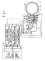
- FIG. 1 is a schematic diagram of a developing device 10 using a non-magnetic type one-component developer and incorporated into an electrophotgraphic printer (not shown).
- the developing device 10 comprises a casing 12 supported by a frame structure of the electrophotographic printing machine in such a manner that the casing 12 is movable toward and away from a photosensitive drum 14 forming a part of the electrophotgraphic printer.
- the photosensitive drum 14 comprises a sleeve substrate 14a made of a conductive material such as aluminum, and a photoconductive material film 14b formed therearound.
- the photoconductive material film 14b of the photosensitive drum 14 may be composed of an organic photoconductor (OPC), a selenium photoconductor or the like.
- OPC organic photoconductor
- a uniform distribution of electrical charges is produced on a surface of the photoconductive material film 14b of the photosensitive drum 14 by a suitable discharger (not shown), such as a corona discharger, and an electrostatic latent image is then optically written on the charged surface of the photoconductive material film 14b by an optical writing means (not shown) such as a laser beam scanner, an LED (light emitting diode) array, a liquid crystal shutter array or the like.
- an optical writing means such as a laser beam scanner, an LED (light emitting diode) array, a liquid crystal shutter array or the like.
- the charges are released from the illuminated zone through the grounded sleeve substrate 14a, so that a potential difference between the illuminated zone and the remaining zone forms the electrostatic latent image.
- the casing 12 includes a vessel 16 for holding a nonmagnetic type one-component developer D composed of colored fine toner particles of a suitable synthetic resin such as polyester or styrene acrylic resin, and having an average diameter of about 10 ⁇ m
- the developing device 10 also comprises an elastic (elastomeric) developing roller 18 rotatably provided within the vessel 16, a portion of which is exposed therefrom.
- the casing 12 is resiliently biased in a direction indicated by an arrow A1, by a suitable resilient element (not shown) such as a coil or leaf spring, so that the exposed portion of the developing roller 18 is resiliently pressed against the surface of the photosensitive drum 14.
- a suitable resilient element such as a coil or leaf spring
- the photosensitive drum 14 and the developing roller 18 are rotated in the directions indicated by arrows A2 and A3, and the developing roller 18 entrains the toner particles to form a developer layer therearound, whereby the toner particles are brought to the surface of the photosensitive drum 14 for the development of the latent image formed thereon.
- the photosensitive drum 14 may have a diameter of 60 mm and a peripheral speed of 70 mm/s.
- the developing roller 18 may have a diameter of 20 mm and a peripheral speed of from 1 to 4 times that of the photosensitive drum
- the developing roller 18 comprises a shaft 18a rotatably supported by the walls of the vessel 16, and a roller element 18b mounted thereon.
- the roller element 18b may be preferably formed of a conductive open-cell foam elastic material such as a conductive open-cell foam polyurethane rubber material, a conductive open-cell foam silicone rubber material, or a conductive open-cell foam acrylonitrile-butadiene rubber material. This is because an elasticity or hardness of the roller element 18b is an important parameter for a proper development of the latent image by the developing rubber roller 18.
- the development quality and the development toner density are greatly affected by a contact or nip width between the photosensitive drum 14 and the developing roller 18 pressed thereagainst, and thus the developing roller 18 must be pressed against the photosensitive drum 14 so that a given nip width by which a proper development is obtained is established therebetween.
- the roller element 18b is formed as a conductive solid rubber roller, it may have a relatively high hardness. For example, when measured by an Asker C-type hardness meter, the solid rubber developing roller showed an Asker C-hardness of about 58°.
- the solid rubber developing roller must be pressed against the photosensitive drum 14 with a relatively high pressure to obtain the required nip width therebetween; but the higher the pressure exerted upon the photosensitive drum 14 by the solid rubber developing roller, the greater the premature wear of the photosensitive drum 14.
- the developing roller 18 is preferably constituted in such a manner that pore openings in the conductive open-cell foam rubber roller element 18b have a diameter which is at most twice the average diameter of the toner particles, whereby a penetration of the toner particles into the porous rubber roller element 18b can be prevented.
- pore openings in the conductive open-cell foam rubber roller element 18b have a diameter which is at most twice the average diameter of the toner particles, whereby a penetration of the toner particles into the porous rubber roller element 18b can be prevented.
- the pore openings in the conductive open-cell foam rubber roller element 18b have a diameter which is at most twice the average diameter of the toner particles, a softness of the roller element 18b can be maintained since it is not hardened by the penetration of the toner particles therein, whereby along operating life of the developing roller can be ensured and a proper development process can be maintained.
- the conductive open-cell foam rubber roller element 18b preferably has a volume resistivity of about 104 to 1010 ⁇ ⁇ m, most preferably 106 ⁇ ⁇ m, and an Asker-C hardness of about 10 to 50°, most preferably 10°.
- the developing roller 18 may be pressed against the photosensitive drum 14 at a linear pressure of about 22 to 50 g/cm, most preferably 43 g/cm, so that a contact or nip width of about 1 to 3.5 mm can be obtained between the developing roller 18 and the photosensitive drum 14. Note, the nip width of about 1 to 3.5 mm is necessary to achieve the proper development of the latent image.
- the developing roller 18 is connected to a DC power source 19 by which a developing bias voltage is supplied thereto.
- the developing device 10 further comprises a blade member 20 engaged with the surface of the developing roller 18 to uniformalize a thickness of the developer layer formed therearound, whereby an even development of the latent image is ensured.
- the blade member 20 is pivotably mounted on a pivot pin 20a supported by the vessel 16, and is resiliently biased in a direction indicated by an arrow A4 so that the blade member 20 is resiliently pressed against the developing roller 18 at a linear pressure of about 26 g/mm, to regulate the thickness of the developer layer formed therearound.
- the vessel 16 is provided with a partition 21 disposed therein adjacent to the blade member 20, and a stopper member 22 made of a foam rubber material or sponge material is disposed between the partition 21 and the blade member 20, so that the developer D is prevented from entering a space therebetween.
- the blade member 20 may be formed of a conductive rubber material, but preferably is coated with Teflon, and may be further formed of a suitable metal material such as aluminum, stainless steel, brass or the like. As shown in Fig. 1, the blade member 20 is connected to a DC power source 23 by which a voltage is supplied thereto so that an electric charge is injected to the toner particles of the developer layer formed around the developing roller 18, and by which an electrostatic adhesion of the toner particles to the blade member 20 is prevented during the regulation of a thickness of the developer layer formed around the developing roller 18.
- the developing device 10 further comprises a toner-removing roller 24 rotatably provided within the vessel 16 and in contact with the developing roller 18 in such a manner that a contact or nip width of about 1 mm is obtained therebetween, and by which remaining toner particles not used for the development of the latent image are removed from the developing roller 18.
- the toner-removing roller 24 is formed of a conductive open-cell foam rubber material; preferably a conductive open-cell foam polyurethane rubber material having a volume resistivity of about 106 ⁇ ⁇ m, and an Asker-C hardness of about 10 to 70°, most preferably 30°.
- the toner-removing roller 24 is rotated in the same direction as the developing roller 18, as indicated by an arrow A5, whereby the remaining toner particles are mechanically removed from the developing roller 18.
- the toner-removing roller 24 may have a diameter of 11 mm and a peripheral speed of from 0.5 to 2 times that of the developing roller 18.
- the toner-removing roller 24 is connected to a DC power source 25 by which a voltage is supplied thereto so that the remaining toner particles also can be electrostatically removed from the developing roller 18.
- the toner-removing roller 24 is partially received in a recess formed in a bottom portion of the vessel 16, whereby a leakage of the toner particles from a space between the developing roller 18 and the vessel bottom can be prevented.
- the developing device 10 comprises a paddle roller 26 for moving the toner particles toward the developing roller 18, and an agitator 28 for agitating the developer D to eliminate a dead stock thereof from the vessel 16.
- the paddle roller 26 and the agitator 28 are rotated in the directions indicated by arrows A6 and A7.
- the developing device 10 is also provided with a drive motor 30 mounted on the casing 12, by which the developing roller 10, the toner-removing roller 24, the paddle roller 26, and the agitator 28 are driven through the intermediary of a gear train (not shown).
- the drive motor 30 is connected to a motor drive circuit 31 by which the motor 30 is driven.
- FIG. 1 also shows a control circuit 32 of the electrophotgraphic printer into which the developing device 10 is incorporated, and by which an ON/OFF control of the DC power sources 19, 23, and 25 and the motor drive circuit 31 is carried out.
- the control circuit 32 also commands the overall operation of the electrophotgraphic printer.
- the control circuit 32 may be constructed by a microcomputer which comprises a central processing unit (CPU) 32a, a read-only memory (ROM) 32b for storing routines, constants, etc., a random access memory (RAM) 32c for storing temporary data, and an input/output interface (I/O) 32d.
- CPU central processing unit
- ROM read-only memory
- RAM random access memory
- I/O input/output interface
- Figure 3 shows a power ON/OFF control routine for the DC power sources 19, 23, and 15 and the motor drive circuit 31, which routine is executed by interruptions output at intervals of 4 ms.
- Figure 4 shows a time chart with relation to the routine of Fig. 2.
- step 201 it is determined whether a flag F1 is "0" or "1". Since the Flag F1 is initially made “0”, the control proceeds to step 202 and it is determined whether or not the printer is ready for writing image data (latent image) on the photosensitive drum 14 by the optical writing means (not shown). If the printer is not ready for the image data writing, the routine is terminated. Although the routine is repeatedly executed at intervals of 4 ms, the control does not proceed from step 202 to step 203 until the printer is ready for the image data writing.
- step 203 in which an ON/OFF signal output from the control circuit 32 to the motor drive circuit 31 rises, as shown in Fig. 3, so that the drive motor 30 is driven to rotate the developing roller 18, the toner-removing roller 24, the paddle roller 26, and the agitator 28.
- step 204 a counter C1 is incremented by 1, and at step 205, it is determined whether or not the count number of the counter C1 is larger than 250. If C1 ⁇ 250, the routine is terminated. Although the routine is repeatedly executed at intervals of 4 ms, the counter C1 is only incremented by 1 until the count number thereof reaches 250.
- the flag F1 is made "1"; at step 210, a flag F2 is made "0"; and at step 211, the counter C1 is reset.
- the developing device 10 carries out a developing process wherein the written image data (latent image) is developed.
- the toner particles are entrained by the developing roller 18 to form a developer layer therearound, and a thickness of the developer layer is uniformly regulated by the blade member 20 while the toner particles of the developer layer are electrically charged by the charge-injection effect resulting from the supply of the voltage of -400 volts to the blade member 20.
- the remaining toner particles not used for the development are mechanically removed from the developing roller 18 by the toner-removing roller 24, but the remaining toner particles also can be electrostatically removed from the developing roller 18 by the supply of a voltage of -250 volts to the toner-removing roller 24 having a higher potential than the developing bias voltage -300 volts of the developing roller 18.
- the DC power source 23 for the blade member 20 is prematurely made OFF, so that the toner particles entrained by the developing roller 18 are electrostatically removed therefrom by the blade member 20; because the negative toner particles are electrostatically attracted to the blade member 20 having the potential (0 volts) higher than that (-300 volts) of the developing roller 18.
- the toner particles can be eliminated from the contacting area between the photosensitive drum 14 and the developing roller 18.
- Figure 4 shows a modification of the embodiment shown in Fig. 1, in which a DC power source 23′ for the blade member 20 is constituted such that an output thereof can be changed from one of two levels of -400 and +200 volts to the other level.
- the photosensitive drum is formed of a selenium photoconductor or an amorphous silicone photoconductor, on which a distribution of positive charges is produced, the toner particles are positively charged and positive voltages are supplied to the developing roller, the blade member, and the toner-removing roller.
- the embodiments of the present invention are explained in relation to a photosensitive drum, they can be also applied to a dielectric drum on which the electrostatic latent image can be formed. Further, although the developing device according to the present invention is used for the non-magnetic type one-component developer, the magnetic type one-compnent developer may be also used, if necessary.
- the developing device is provided with the toner-removing roller, it may be omitted therefrom, if necessary.
Abstract
Description
- The present invention relates to electrophotographic developing apparatus.
- An electrophotographic printer generally carries out the processes of: producing a uniform distribution of electrical charges on a surface of an electrostatic latent image carrying body such as an electrophotographic photoreceptor; forming an electrostatic latent image on the electrically charged surface of the electrophotographic photoreceptor by optically writing an image thereon, using a laser beam scanner, an LED (light emitting diode) array, an LCS (liquid crystal shutter) array or the like; visually developing the electrostatic latent image with a developer, i.e., toner, which is electrically charged to be electrostatically adhered to the electostatic latent image zone; electrostatically transferring the developed visible image to a paper; and fixing the transferred image on the paper. Typically, the electrophotographic photoreceptor is formed as a photosensitive drum having a cylindrical conductive substrate and a photoconductive insulating film bonded to a cylindrical surface thereof.
- In the developing process, a two-component developer composed of a toner component (colored fine synthetic resin particles) and a magnetic component (magnetic fine carriers) is widely used, as it enables a stable development of the latent image. Note, typically the toner particles have an average diameter of about 10 µm, and the magnetic fine carriers have a diameter ten times larger than the average diameter of the toner particles. Usually, a developing device using the two-component developer includes a vessel for holding the two-component developer, wherein the developer is agitated by an agitator provided therein. This agitation causes the toner particles and the magnetic carriers to be subjected to triboelectrification, whereby the toner particles are electrostatically adhered to each of the magnetic carriers. The developing device also includes a magnetic roller, provided in the vessel as a developing roller, in such a manner that a portion of the magnetic roller is exposed therefrom and faces the surface of the photosensitive drum. The magnetic carriers with the toner particles are magnetically adhered to the surface of the magnetic roller to form a magnetic brush therearound, and by rotating the magnetic roller carrying the magnetic brush, the toner particles are brought to the surface of the photosensitive drum for the development of the electrostatic latent image formed theron.
- In this developing device, a ratio between the toner and magnetic components of the developer body held in the vessel must fall within a predetermined range, to continuously maintain a stable development process. Accordingly, the developing device is provided with a toner supplier from which a toner component is supplied to the two-component developer held in the vessel, to supplement the toner component as it is consumed during the development process, whereby the component ratio of the two-component developer held by the vessel is kept within the predetermined range. This use of a two-component developer is advantageous in that a stable development process is obtained thereby, but the developing device per se has the disadvantages of a cumbersome control of a suitable component ratio of the two-component developer, and an inability to reduce the size of the developing device due to the need to incorporate the toner supplier therein.
- A one-component developer is also known in this field, and a developing device using same does not suffer from the above-mentioned disadvantages of the developing device using the two-component developer, because the one-component developer is composed of only a toner component (colored fine synthetic resin particles). Two types of the one-component developer are known; a magnetic type and a non-magnetic type. A developing device using the magnetic type one-component developer can be constructed in substantially the same manner as that using the two-component developer. Namely, the magnetic type one-component developer also can be brought to the surface of the photosensitive drum by a rotating magnetic roller as in the developing device using the two-component developer. The magnetic type one-component developer is suitable for achromatic color (black) printing, but is not suitable for chromatic color printing. This is because each of the toner particles composing the magnetic type one-component developer includes fine magnetic powders having a dark color. In particular, the chromatic color printing obtained from the magnetic type one-component developer appears dark and dull, due to the fine magnetic powders included therein. Conversely, the non-magnetic type one-component developer is particularly suitable for chromatic color printing because it does not include a substance having a dark color, but the non-magnetic type one-component developer cannot be brought to the surface of the photosensitive drum by the magnetic roller as mentioned above.
- A developing device using the non-magnetic type one-component developer is also known, as disclosed in U.S. Patents No. 3,152,012 and No. 3,754,963, Japanese Examined Patent Publication (Kokoku) No.60-12627, and Japanese Unexamined Patent Publications (Kokai) No. 62-976, No. 62-118372, No. 63- 100482, and No. 63-189876. These developing devices include a vessel for holding the non-magnetic type one-component developer, and a conductive elastic roller provided within the vessel as a developing roller in such a manner that a portion of the elastic roller is exposed therefrom and can be pressed against the surface of the photosensitive drum. The conductive elastic developing roller may be formed of a conductive silicone rubber material or a conductive polyurethane rubber material or the like. When the conductive rubber roller is rotated within the body of the non-magnetic type one-component developer held by the vessel, the toner particles composing the non-magnetic type one-component developer are frictionally entrained by the surface of the conductive rubber developing roller to form a developer layer therearound, whereby the toner particles can be brought to the surface of the photosensitive drum for the development of the electrostatic latent image formed thereon. In this developing device, the development process is carried out in such a manner that, at the area of contact between the photosensitive drum and the conductive rubber developing roller carrying the developer layer, the charged toner particles are electrostatically attracted and adhered to the latent image due to a bias voltage supplied to the conductive solid rubber developing roller.
- The developing device further includes a blade member which is resiliently pressed against the surface of the developing roller, to uniformly regulate a thickness of the developer layer formed therearound so that an even development of the latent image can be carried out. The blade member may be also used to electrically charge the toner particles by a triboelectrification therebetween and/or by a charge-injection effect resulting from supply of voltage to the conductive blade member. Of course, when the charge-injection effect is utilized, the blade member is formed of a conductor such as a conductive rubber material, aluminum, stainless steel, brass or the like. The supply of voltage to the blade member also serves to prevent an electrostatical adhesion of the toner particles to the blade member during the regulation of a thickness of the developer layer formed around the developing roller.
- The developing device may be also provided with a toner-developing roller which is rotated in contact with the developing roller so that remaining toner particles not used for the development of the latent image are mechanically removed from the developing roller, whereby a fresh developer layer can be continuously formed on the surface of the developing roller. Note, the developer layer formed of the remaining toner particles not used for the development of the latent image should be once removed from the developing roller because it is subjected to physical and electrical affects during the developing process, and thus prevents a physical and electrical even formation of the developer layer around the developing roller. The toner-removing roller can be formed of a conductive porous rubber material, so that the remaining toner particles not used during the development of the latent image can be also electrostatically removed from the developing roller. In particular, a voltage is supplied to the conductive toner-removing roller so that the charged toner particles are electrostatically attracted from the developing roller to the toner-removing roller, whereby not only the mechanical removal of the remaining toner particles but also the electrostatic removal thereof can be carried out.
- Conventionally, when a drive moter is driven for the rotation of the developing roller, the voltages are simultaneously supplied to the developing roller, the blade member, and the toner-removing roller, respectively. Nevertheless, the rotation of the developing roller cannot be started at exactly the same time as voltages are supplied to the developing roller, the blade member, and the toner-removing roller, due to a backlash of a gear train provided between the drive motor and the developing roller. Namely, before the rotation of the developing roller is started, the voltages are supplied to the developing roller, the blade member, and the toner-removing roller, and thus a high electrical current flows at localized contacting zones between the developing roller and the blade member and toner-removing roller, resulting in a fusion of the developing roller at the localized contacting zones due to the generation of Joule heat. Of course, when the surface of the developing roller is damaged, the quality of a developed image (and thus a printed image) is deteriorated.
- Also conventionally, when the developing device is in a non-operative condition, the developer layer formed around the developing roller is left as it is. Accordingly, the toner particles existing between the photosensitive drum and the developing roller may be adhered not only to each other but also to the surface of the photosensitive drum, because the developing roller is resiliently pressed against the photosensitive drum, and thus when the developing device is again operated the quality of a printed image is deteriorated.
- It is desirable to provide a developing device, of the type mentioned above, in which a high electrical current cannot flow at localized contacting zones between the developing roller and the blade member and toner-removing roller.
- It is also desirable to provide a developing device, of the type mentioned above, such that toner particles do not remain between the photosensitive drum and developing roller at the end of a development cycle.
- An embodiment of the present invention can provide a developing device using a one-component developer composed of toner particles, which device comprises a vessel for holding the developer, and a developing roller rotatably provided within and supported by the vessel in such a manner that a portion of the developing roller is exposed therefrom. The exposed portion of the developing roller is pressed against a surface of an electrostatic latent image carrying body, and the developing roller is formed of a conductive elastic (elastomeric) aerial by which the toner particles are entrained to form a developer layer therearound and are carried to the surface of the electrostatic latent image carrying body for development of an electrostatic latent image formed thereon. The developing roller is rotated by a drive motor which is driven by a motor drive circuit. A blade member is provided within the vessel and is pressed against the developing roller for regulating a thickness of the developer layer formed therearound. A developing bias voltage is supplied from a first power source to the developing roller, and a voltage is supplied from a second power source to the blade member to inject an electric charge to the toner particles of the developer layer and/or to prevent an electrostatic adhesion of the toner particles to the blade member. When the developing device is operated, the first and second power sources and the motor drive circuit are controlled in such a manner that the supply of the voltages to the developing roller and the blade member is carried out after the developing roller is rotated by the drive motor. Alternatively or in addition, when the operation of the developing device is interrupted or stopped, the first and second power sources and the motor drive circuit are controlled in such a manner that the supply of the voltage to the blade member is prematurely stopped before the supply of the voltage to the developing roller and the rotation of the developing roller are stopped.
- The developing device may comprise a toner-removing roller rotatably provided within and supported by the vessel in such a manner that it is resiliently pressed against the developing roller, the toner-removing roller being formed of a conductive elastic material and being rotated so that remaining toner particles not used for the development of the latent image are mechanically removed from the developing roller, and a third power source for supplying a voltage to the toner-removing roller to electrostatically remove the remaining toner particles from the developing roller. In this case, when the developing device is operated, the first, second, and third power sources and the motor drive circuit are controlled in such a manner that the supply of the voltages to the developing roller, blade member, and toner-removing roller is carried out after the developing roller is rotated by the drive motor. When the operation of the developing device is interrupted or stopped, the first, second, and third power sources and the motor drive circuit are controlled in such a manner that the supply of the voltage to the blade member is prematurely stopped before the supply of the voltages to the developing roller and toner-removing roller and the rotation of the developing roller are stopped.
- The second power source for the blade member may be constituted so that one of first and second voltages is selectively supplied to the blade member, the first voltage having a polarity opposite to that of the second voltage. The first voltage is supplied to the blade member to inject an electric charge to the toner particles of the developer layer and/or to prevent an electrostatic adhesion of the toner particles to the blade member during the development of the latent image, the second voltage is supplied to the blade member to electrostatically remove the toner particles of the developer layer from the developing roller after the development of the latent image is completed. In this case, when the developing device is operated, the first and second power sources and the motor drive circuit are controlled in such a manner that a change of the supply of the first voltage to the supply of the second voltage is carried out before the supply of the voltage to the developing roller and the rotation of the developing roller are stopped. When the operation of the developing device is interrupted or stopped, the first and second power sources and the motor drive circuit are controlled in such a manner that a change of the supply of the first voltage to the supply of the second voltage is carried out before the supply of the voltage to the developing roller and the rotation of the developing roller are stopped.
- Preferably, the developing roller is formed of a conductive open-cell foam material so that pore openings are formed over a surface of the developing roller, the pore openings having a diameter which is at most twice an average diameter of the toner particles. The conductive open-cell foam material of the developing roller may be selected from the group consisting of a conductive polyurethane open-cell foam rubber material, a conductive silicone foam rubber material, and a conductive acrylonitorile-butadiene open-cell foam rubber material. Also, the toner- removing roller is preferably formed of a conductive open-cell foam rubber material.
- Reference will now be made, by way of example, to the accompanying drawings, in which:
- Figure 1 is a schematic diagram of a developing device embodying the present invention;
- Figure 2 is a flow chart for explaining an operation of the developing device of Fig. 1;
- Figure 3 is a time chart corresponding to the flow chart of Fig. 2;
- Figure 4 is a partial schematic diagram of a modification of the embodiment shown in Fig. 1;
- Figure 5 is a partial flow chart for explaining an operation of the modified embodiment of Fig. 4; and
- Figure 6 is a time chart corresponding to the flow chart of Fig. 5;
- Figure 1 is a schematic diagram of a developing
device 10 using a non-magnetic type one-component developer and incorporated into an electrophotgraphic printer (not shown). The developingdevice 10 comprises acasing 12 supported by a frame structure of the electrophotographic printing machine in such a manner that thecasing 12 is movable toward and away from aphotosensitive drum 14 forming a part of the electrophotgraphic printer. Thephotosensitive drum 14 comprises a sleeve substrate 14a made of a conductive material such as aluminum, and aphotoconductive material film 14b formed therearound. Thephotoconductive material film 14b of thephotosensitive drum 14 may be composed of an organic photoconductor (OPC), a selenium photoconductor or the like. A uniform distribution of electrical charges is produced on a surface of thephotoconductive material film 14b of thephotosensitive drum 14 by a suitable discharger (not shown), such as a corona discharger, and an electrostatic latent image is then optically written on the charged surface of thephotoconductive material film 14b by an optical writing means (not shown) such as a laser beam scanner, an LED (light emitting diode) array, a liquid crystal shutter array or the like. In particular, when the charged area of thephotoconductive material film 14b is illuminated by the optical writing means, the charges are released from the illuminated zone through the grounded sleeve substrate 14a, so that a potential difference between the illuminated zone and the remaining zone forms the electrostatic latent image. Thecasing 12 includes avessel 16 for holding a nonmagnetic type one-component developer D composed of colored fine toner particles of a suitable synthetic resin such as polyester or styrene acrylic resin, and having an average diameter of about 10 µm. - The developing
device 10 also comprises an elastic (elastomeric) developingroller 18 rotatably provided within thevessel 16, a portion of which is exposed therefrom. Thecasing 12 is resiliently biased in a direction indicated by an arrow A₁, by a suitable resilient element (not shown) such as a coil or leaf spring, so that the exposed portion of the developingroller 18 is resiliently pressed against the surface of thephotosensitive drum 14. During an operation of the developing device, thephotosensitive drum 14 and the developingroller 18 are rotated in the directions indicated by arrows A₂ and A₃, and the developingroller 18 entrains the toner particles to form a developer layer therearound, whereby the toner particles are brought to the surface of thephotosensitive drum 14 for the development of the latent image formed thereon. For example, thephotosensitive drum 14 may have a diameter of 60 mm and a peripheral speed of 70 mm/s. Further, the developingroller 18 may have a diameter of 20 mm and a peripheral speed of from 1 to 4 times that of thephotosensitive drum 14. - The developing
roller 18 comprises ashaft 18a rotatably supported by the walls of thevessel 16, and aroller element 18b mounted thereon. Theroller element 18b may be preferably formed of a conductive open-cell foam elastic material such as a conductive open-cell foam polyurethane rubber material, a conductive open-cell foam silicone rubber material, or a conductive open-cell foam acrylonitrile-butadiene rubber material. This is because an elasticity or hardness of theroller element 18b is an important parameter for a proper development of the latent image by the developingrubber roller 18. In particular, the development quality and the development toner density are greatly affected by a contact or nip width between thephotosensitive drum 14 and the developingroller 18 pressed thereagainst, and thus the developingroller 18 must be pressed against thephotosensitive drum 14 so that a given nip width by which a proper development is obtained is established therebetween. If theroller element 18b is formed as a conductive solid rubber roller, it may have a relatively high hardness. For example, when measured by an Asker C-type hardness meter, the solid rubber developing roller showed an Asker C-hardness of about 58°. Accordingly, the solid rubber developing roller must be pressed against thephotosensitive drum 14 with a relatively high pressure to obtain the required nip width therebetween; but the higher the pressure exerted upon thephotosensitive drum 14 by the solid rubber developing roller, the greater the premature wear of thephotosensitive drum 14. - Furthermore, the developing
roller 18 is preferably constituted in such a manner that pore openings in the conductive open-cell foamrubber roller element 18b have a diameter which is at most twice the average diameter of the toner particles, whereby a penetration of the toner particles into the porousrubber roller element 18b can be prevented. This is because, for example, when the two toner particles having the 10 µm diameter are captured by the pore opening having the 20 µm diameter, these toner particles interfere with each other in such a manner they are prevented from penetrating into the open-cell foam structure of theroller element 18b. Namely, when the pore openings in the conductive open-cell foamrubber roller element 18b have a diameter which is at most twice the average diameter of the toner particles, a softness of theroller element 18b can be maintained since it is not hardened by the penetration of the toner particles therein, whereby along operating life of the developing roller can be ensured and a proper development process can be maintained. - The conductive open-cell foam
rubber roller element 18b preferably has a volume resistivity of about 10⁴ to 10¹⁰ Ω · m, most preferably 10⁶ Ω · m, and an Asker-C hardness of about 10 to 50°, most preferably 10°. The developingroller 18 may be pressed against thephotosensitive drum 14 at a linear pressure of about 22 to 50 g/cm, most preferably 43 g/cm, so that a contact or nip width of about 1 to 3.5 mm can be obtained between the developingroller 18 and thephotosensitive drum 14. Note, the nip width of about 1 to 3.5 mm is necessary to achieve the proper development of the latent image. As shown in Fig. 1, the developingroller 18 is connected to aDC power source 19 by which a developing bias voltage is supplied thereto. - The developing
device 10 further comprises ablade member 20 engaged with the surface of the developingroller 18 to uniformalize a thickness of the developer layer formed therearound, whereby an even development of the latent image is ensured. Theblade member 20 is pivotably mounted on apivot pin 20a supported by thevessel 16, and is resiliently biased in a direction indicated by an arrow A₄ so that theblade member 20 is resiliently pressed against the developingroller 18 at a linear pressure of about 26 g/mm, to regulate the thickness of the developer layer formed therearound. Thevessel 16 is provided with apartition 21 disposed therein adjacent to theblade member 20, and astopper member 22 made of a foam rubber material or sponge material is disposed between thepartition 21 and theblade member 20, so that the developer D is prevented from entering a space therebetween. Theblade member 20 may be formed of a conductive rubber material, but preferably is coated with Teflon, and may be further formed of a suitable metal material such as aluminum, stainless steel, brass or the like. As shown in Fig. 1, theblade member 20 is connected to aDC power source 23 by which a voltage is supplied thereto so that an electric charge is injected to the toner particles of the developer layer formed around the developingroller 18, and by which an electrostatic adhesion of the toner particles to theblade member 20 is prevented during the regulation of a thickness of the developer layer formed around the developingroller 18. - The developing
device 10 further comprises a toner-removingroller 24 rotatably provided within thevessel 16 and in contact with the developingroller 18 in such a manner that a contact or nip width of about 1 mm is obtained therebetween, and by which remaining toner particles not used for the development of the latent image are removed from the developingroller 18. The toner-removingroller 24 is formed of a conductive open-cell foam rubber material; preferably a conductive open-cell foam polyurethane rubber material having a volume resistivity of about 10⁶ Ω · m, and an Asker-C hardness of about 10 to 70°, most preferably 30°. The toner-removingroller 24 is rotated in the same direction as the developingroller 18, as indicated by an arrow A₅, whereby the remaining toner particles are mechanically removed from the developingroller 18. For example, the toner-removingroller 24 may have a diameter of 11 mm and a peripheral speed of from 0.5 to 2 times that of the developingroller 18. As shown in Fig. 1, the toner-removingroller 24 is connected to aDC power source 25 by which a voltage is supplied thereto so that the remaining toner particles also can be electrostatically removed from the developingroller 18. Note, the toner-removingroller 24 is partially received in a recess formed in a bottom portion of thevessel 16, whereby a leakage of the toner particles from a space between the developingroller 18 and the vessel bottom can be prevented. - Furthermore, the developing
device 10 comprises apaddle roller 26 for moving the toner particles toward the developingroller 18, and anagitator 28 for agitating the developer D to eliminate a dead stock thereof from thevessel 16. Thepaddle roller 26 and theagitator 28 are rotated in the directions indicated by arrows A₆ and A₇. The developingdevice 10 is also provided with adrive motor 30 mounted on thecasing 12, by which the developingroller 10, the toner-removingroller 24, thepaddle roller 26, and theagitator 28 are driven through the intermediary of a gear train (not shown). Thedrive motor 30 is connected to amotor drive circuit 31 by which themotor 30 is driven. - Figure 1 also shows a
control circuit 32 of the electrophotgraphic printer into which the developingdevice 10 is incorporated, and by which an ON/OFF control of theDC power sources motor drive circuit 31 is carried out. Note, as is obvious, thecontrol circuit 32 also commands the overall operation of the electrophotgraphic printer. As illustrated, thecontrol circuit 32 may be constructed by a microcomputer which comprises a central processing unit (CPU) 32a, a read-only memory (ROM) 32b for storing routines, constants, etc., a random access memory (RAM) 32c for storing temporary data, and an input/output interface (I/O) 32d. - The operation of the developing
device 10 will be now explained with reference to Figures 2 and 3. The operation may be carried out, for example, under the following conditions: - (1) The
photosensitive film 14b of thephotosensitive drum 14 is formed of an organic photoconductor (OPC), and a distribution of a negative charge is produced thereon, a charged area of which may have a potential of about -650 volts. In this case, the latent image zone formed on thedrum 14 by the optical writing means may have a potential of about -50 volts. On the other hand, the toner particles are given a negative charge. - (2) The developing
roller 18 is rotated at a peripheral speed of 175 mm/s, and a developing bias voltage of -300 volts is supplied by theDC power source 19 to the developingroller 18. - (3) A voltage of -400 volts is supplied by the
DC power source 23 to theblade member 20. - (4) A voltage of -250 volts is supplied by the
DC power source 25 to the toner-removingroller 24. - Figure 3 shows a power ON/OFF control routine for the
DC power sources motor drive circuit 31, which routine is executed by interruptions output at intervals of 4 ms. Figure 4 shows a time chart with relation to the routine of Fig. 2. - At
step 201, it is determined whether a flag F₁ is "0" or "1". Since the Flag F₁ is initially made "0", the control proceeds to step 202 and it is determined whether or not the printer is ready for writing image data (latent image) on thephotosensitive drum 14 by the optical writing means (not shown). If the printer is not ready for the image data writing, the routine is terminated. Although the routine is repeatedly executed at intervals of 4 ms, the control does not proceed fromstep 202 to step 203 until the printer is ready for the image data writing. - For example, when the printer is ready for the image data writing at a time of T₁ (Fig. 3), the control proceeds to step 203, in which an ON/OFF signal output from the
control circuit 32 to themotor drive circuit 31 rises, as shown in Fig. 3, so that thedrive motor 30 is driven to rotate the developingroller 18, the toner-removingroller 24, thepaddle roller 26, and theagitator 28. Then, at step 204, a counter C₁ is incremented by 1, and atstep 205, it is determined whether or not the count number of the counter C₁ is larger than 250. If C₁< 250, the routine is terminated. Although the routine is repeatedly executed at intervals of 4 ms, the counter C₁ is only incremented by 1 until the count number thereof reaches 250. - At
step 205, when the count number of the counter C₁ reaches 250, i.e., 1 second has elapsed, the control successively proceeds tosteps control circuit 32 to theDC power sources roller 18, theblade member 20, and the toner-removingroller 24, respectively. Then, atstep 209, the flag F₁ is made "1"; at step 210, a flag F₂ is made "0"; and at step 211, the counter C₁ is reset. - Thereafter, even if the routine is repeatedly executed at intervals of 4 ms, the control is only returned through
steps 201 and 212 (F₁ = 1) until the image data writing is completed. During this period, the developingdevice 10 carries out a developing process wherein the written image data (latent image) is developed. In particular, the toner particles are entrained by the developingroller 18 to form a developer layer therearound, and a thickness of the developer layer is uniformly regulated by theblade member 20 while the toner particles of the developer layer are electrically charged by the charge-injection effect resulting from the supply of the voltage of -400 volts to theblade member 20. Note, an electrostatic adhesion of the negative toner particles to the blade member is prevented because the blade member has a lower potential (-400 volts) than that (-300 volts) of the developingroller 18. Then, when the developer layer having the regulated thickness is carried to the surface of thephotosensitive drum 14, the toner particles are electrostatically attracted only to the latent image zone having the potential of about -50 volts, due to the supply of the developing bias voltage of -300 volts to the developingroller 18, as if the latent image zone were charged with the negative toner particles, and thus the toner development of the latent image is carried out. The remaining toner particles not used for the development are mechanically removed from the developingroller 18 by the toner-removingroller 24, but the remaining toner particles also can be electrostatically removed from the developingroller 18 by the supply of a voltage of -250 volts to the toner-removingroller 24 having a higher potential than the developing bias voltage -300 volts of the developingroller 18. - When the routine is executed after the image data writing is completed at, for example, a time of T₃, as shown in Fig. 3, the control proceeds from
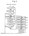
step 212 to step 213, in which it is determined whether the flag F₂ is "0" or "1". Since the flag F₂ = 0, the control proceeds to step 214 in which a counter C₂ is incremented by 1, and atstep 215, it is determined whether or not the count number of the counter C₂ is larger than 125. If C₂< 125, the routine is once completed. Although the routine is repeatedly executed at intervals of 4 ms, the counter C₂ is only incremented by 1 until the count number thereof reaches 125. - At
step 215, when the count number of the counter C₂ reaches 125, i.e., 0.5 second has elapsed, the control proceeds to step 216, at which the power ON/OFF signal PSB falls at a time of T₄ (T₃ - T₄ = 0.5 sec.), as shown in Fig. 3, so that thepower source 23 for theblade member 20 is made OFF. During this time of 0.5 second, the last written image data (latent image) is developed. Then, at step 217, the flag F₂ is made "1", and atstep 218, the counter C₂ is reset. - Subsequently, the control proceeds to step 219 in which a counter C₃ is incremented by 1, and at
step 220, it is determined whether or not the count number of the counter C₃ is larger than 125. If C₃< 125, the routine is once completed. Although the routine is repeatedly executed at intervals of 4 ms, the counter C₃ is only incremented by 1 until the count number thereof reaches 125 (Note, F₂ = 1). - At
step 220, when the count number of the counter C₃ reaches 125, i.e., 0.5 second has elapsed, the control successively proceeds tosteps power sources motor drive circuit 31 are made OFF. Then, at step 224, the flag F₁ is made "0", and at step 225, the counter C₃ is reset. - As apparent from the above description, since the supply of the voltages to the developing
roller 18, theblade member 20, and the toner-removingroller 24 is carried out after the time of 1 second has elapsed (i.e., after the rotation of the developingroller 18 is started), a high electrical current flow cannot occur at localized contacting zones between the developingroller 18 and theblade member 20 and toner-removingroller 24. Also, when a developing operation of the developingdevice 10 is interrupted or stopped, theDC power source 23 for theblade member 20 is prematurely made OFF, so that the toner particles entrained by the developingroller 18 are electrostatically removed therefrom by theblade member 20; because the negative toner particles are electrostatically attracted to theblade member 20 having the potential (0 volts) higher than that (-300 volts) of the developingroller 18. As a result, during the non-operative condition of the developingdevice 10, the toner particles can be eliminated from the contacting area between thephotosensitive drum 14 and the developingroller 18. - Figure 4 shows a modification of the embodiment shown in Fig. 1, in which a
DC power source 23′ for theblade member 20 is constituted such that an output thereof can be changed from one of two levels of -400 and +200 volts to the other level. - The operation of the modified embodiment of Fig. 4 will be now explained with reference to Figures 5 and 6. Note, the routine of Figure 5 is partially shown, but the whole thereof can be seen with reference to Fig. 2. Figure 6 is a time chart with relation to the routine of Fig. 5.
- As explained with reference to Fig. 2, in this operation, an ON/OFF signal DS output from the
control circuit 32 to themotor drive circut 31 also rises at a time of T₁ (Fig. 6) when the printer is ready for the image data writing, so that thedrive motor 30 is driven to rotate the developingroller 18, the toner-removingroller 24, thepaddle roller 26, and theagitator 28, and then power ON/OFF signals PSB, PST, and PSD output from thecontrol circuit 32 to theDC power sources roller 18, theblade member 20, and the toner-removingroller 24, respectively. - When the routine is executed after the image data writing is completed at a time of T₃, as shown in Fig. 6, the control proceeds from
step 212 to step 501, in which it is determined whether the flag F₂ is"0" or "1". Since the flag F₂ = 0, the control proceeds to step 502 in which a counter C₂ is incremented by 1, and atstep 503, it is determined whether or not the count number of the counter C₂ is larger than 125. If C₂ < 125, the routine is once completed. Although the routine is repeatedly executed at intervals of 4 ms, the counter C₂ is only incremented by 1 until the count number thereof reaches 125. - At
step 503, when the count number of the counter C₂ reaches 125, i.e., 0.5 second has elapsed, the control proceeds to step 504, at which a change signal CS output from thecontrol circuit 32 to theDC power source 23′ rises at a time of T₄ (T₃ - T₄ = 0.5 sec.), as shown in Fig. 6, so that the output level of theDC power source 23′ is changed from -400 volts to +200 volts. During this time of 0.5 second, the last written image data (latent image) is developed. Then, atstep 504, the flag F₂ is made "1", and atstep 506, the counter C₂ is reset. - Subsequently, the control proceeds to step 507 in which a counter C₃ is incremented by 1, and at
step 508, it is determined whether or not the count number of the counter C₃ is larger than 125. If C₃< 125, the routine is once completed. Although the routine is repeatedly executed at intervals of 4 ms, the counter C₃ is only incremented by 1 until the count number thereof reaches 125 (Note, F₂ = 1). - At
step 508, when the count number of the counter C₃ reaches 125, i.e., 0.5 second has elapsed, the control successively proceeds tosteps power sources motor drive circuit 31. are made OFF. Then, atstep 514, the flag F₁ is made "0", and atstep 515, the counter C₃ is reset. - In the modified embodiment of Fig. 4, when a developing operation of the developing
device 10 is stopped, the positive voltage of +200 volts is supplied to theblade member 20 so that the negative toner particles can be removed from the developingroller 18 with a larger electrostatic attraction. - When the photosensitive drum is formed of a selenium photoconductor or an amorphous silicone photoconductor, on which a distribution of positive charges is produced, the toner particles are positively charged and positive voltages are supplied to the developing roller, the blade member, and the toner-removing roller.
- Although the embodiments of the present invention are explained in relation to a photosensitive drum, they can be also applied to a dielectric drum on which the electrostatic latent image can be formed. Further, although the developing device according to the present invention is used for the non-magnetic type one-component developer, the magnetic type one-compnent developer may be also used, if necessary.
- Also, in the embodiments as mentioned above, although the developing device is provided with the toner-removing roller, it may be omitted therefrom, if necessary.
- Finally, it will be understood by those skilled in the art that the foregoing description is of preferred embodiments of the present invention, and that various changes and modifications can be made thereto without departing from the spirit and scope thereof.
Claims (10)
characterised in that operation of the said control means is such that the application of the said bias voltages is delayed for a preset period of time (T₂-T₁) after initiation of the said rotation, thereby to reduce the danger of localised damage due to electrical current flow between the said blade member and the developing roller prior to attainment of its normal speed of rotation.
characterised in that operation of the said control means is such that when the said rotation is to be stopped, by termination of a drive signal (DS) maintaining that rotation, the application of the said second bias voltage is terminated at a first instant (T₄) whereafter the said drive signal is terminated at a second instant (T₅), a predetermined short period of time after the said first instant, the application of the said developing bias voltage being maintained until the said second instant, thereby to encourage separation of toner particles from the roller during the said predetermined short period.
Applications Claiming Priority (4)
| Application Number | Priority Date | Filing Date | Title |
|---|---|---|---|
| JP159319/89 | 1989-06-21 | ||
| JP1159319A JPH0324569A (en) | 1989-06-21 | 1989-06-21 | Developing device |
| JP167642/89 | 1989-06-29 | ||
| JP1167642A JP2863201B2 (en) | 1989-06-29 | 1989-06-29 | Developing device |
Publications (3)
| Publication Number | Publication Date |
|---|---|
| EP0404561A2 true EP0404561A2 (en) | 1990-12-27 |
| EP0404561A3 EP0404561A3 (en) | 1992-04-15 |
| EP0404561B1 EP0404561B1 (en) | 1994-01-12 |
Family
ID=26486161
Family Applications (1)
| Application Number | Title | Priority Date | Filing Date |
|---|---|---|---|
| EP90306778A Expired - Lifetime EP0404561B1 (en) | 1989-06-21 | 1990-06-21 | Electrophotographic developing apparatus |
Country Status (5)
| Country | Link |
|---|---|
| US (1) | US5164773A (en) |
| EP (1) | EP0404561B1 (en) |
| KR (1) | KR930011437B1 (en) |
| AU (1) | AU619686B2 (en) |
| DE (1) | DE69005920T2 (en) |
Cited By (3)
| Publication number | Priority date | Publication date | Assignee | Title |
|---|---|---|---|---|
| EP0522813A2 (en) * | 1991-07-06 | 1993-01-13 | Fujitsu Limited | Electrophotographic recording apparatus |
| EP0547238A1 (en) * | 1991-07-06 | 1993-06-23 | Fujitsu Limited | Developing device using a one-pack developing agent |
| EP2998796A1 (en) * | 2014-09-22 | 2016-03-23 | Oki Data Corporation | Image forming apparatus |
Families Citing this family (16)
| Publication number | Priority date | Publication date | Assignee | Title |
|---|---|---|---|---|
| JPH0363677A (en) * | 1989-08-01 | 1991-03-19 | Fujitsu Ltd | Developing device with one-component toner |
| JP2848547B2 (en) * | 1991-11-06 | 1999-01-20 | 富士通株式会社 | Image forming apparatus roller and image forming apparatus using the same |
| JP2987254B2 (en) * | 1992-05-29 | 1999-12-06 | 株式会社東芝 | Developing device and image forming device |
| EP0590768B1 (en) * | 1992-09-28 | 1999-03-03 | Fujitsu Limited | Image formation apparatus and conductive rubber roller for use therein |
| JP2991317B2 (en) * | 1993-03-19 | 1999-12-20 | 富士通株式会社 | Image forming device |
| JP3070899B2 (en) * | 1994-09-09 | 2000-07-31 | 沖電気工業株式会社 | Electrophotographic developing device |
| JP3389472B2 (en) * | 1997-09-04 | 2003-03-24 | シャープ株式会社 | One-component toner developing device |
| US6353720B1 (en) | 1999-10-07 | 2002-03-05 | Sharp Kabushiki Kaisha | Image developing device using a toner as a developer |
| KR100449987B1 (en) * | 2002-11-19 | 2004-09-24 | 삼성전자주식회사 | developer-supplying apparatus of image forming device |
| US7013104B2 (en) | 2004-03-12 | 2006-03-14 | Lexmark International, Inc. | Toner regulating system having toner regulating member with metallic coating on flexible substrate |
| US7236729B2 (en) | 2004-07-27 | 2007-06-26 | Lexmark International, Inc. | Electrophotographic toner regulating member with induced strain outside elastic response region |
| JP2009098631A (en) * | 2007-09-26 | 2009-05-07 | Oki Data Corp | Image forming apparatus |
| US8005381B2 (en) * | 2007-09-26 | 2011-08-23 | Oki Data Corporation | Image forming apparatus |
| JP5274162B2 (en) * | 2008-09-05 | 2013-08-28 | キヤノン株式会社 | Image forming apparatus |
| EP3317727B1 (en) | 2015-12-22 | 2021-07-28 | Hp Indigo B.V. | Photoconductor refreshing cycles |
| US10534291B2 (en) * | 2017-10-26 | 2020-01-14 | Hewlett-Packard Development Company, L.P. | Image forming system with developer retainer |
Citations (5)
| Publication number | Priority date | Publication date | Assignee | Title |
|---|---|---|---|---|
| US4286543A (en) * | 1978-05-16 | 1981-09-01 | Ricoh Company, Ltd. | Apparatus for developing electrostatic image |
| GB2163371A (en) * | 1984-08-07 | 1986-02-26 | Ricoh Kk | Developing electrostatic latent images |
| JPS61173273A (en) * | 1985-01-29 | 1986-08-04 | Fuji Xerox Co Ltd | Developing device |
| US4745429A (en) * | 1986-09-30 | 1988-05-17 | Kabushiki Kaisha Toshiba | Developing apparatus for an electrostatic photocopier |
| US4755847A (en) * | 1985-08-23 | 1988-07-05 | Ricoh Company, Ltd. | Electrostatic latent image developing apparatus |
Family Cites Families (28)
| Publication number | Priority date | Publication date | Assignee | Title |
|---|---|---|---|---|
| JPS53138349A (en) * | 1977-05-10 | 1978-12-02 | Ricoh Co Ltd | Powder toner feeding member |
| JPS54137346A (en) * | 1978-04-18 | 1979-10-25 | Ricoh Co Ltd | Development of electrostatic latent image |
| JPS5577764A (en) * | 1978-12-07 | 1980-06-11 | Toshiba Corp | Pressure developing device |
| JPS57120947A (en) * | 1981-01-20 | 1982-07-28 | Canon Inc | Method for development |
| GB2138565B (en) * | 1983-03-25 | 1986-10-22 | Central Electr Generat Board | Apparatus for monitoring particulate matter |
| DE3321836A1 (en) * | 1983-06-15 | 1984-12-20 | Siemens AG, 1000 Berlin und 8000 München | ENCLOSED, PRESSURE GAS INSULATED HIGH VOLTAGE SWITCHGEAR |
| US4743937A (en) * | 1983-12-12 | 1988-05-10 | Xerox Corporation | Apparatus for charging toner particles |
| JPH0619630B2 (en) * | 1984-08-08 | 1994-03-16 | 株式会社リコー | Development device |
| US4760422A (en) * | 1985-01-16 | 1988-07-26 | Ricoh Company, Ltd. | Developing device using single component toner |
| US4788570A (en) * | 1985-04-15 | 1988-11-29 | Ricoh Company, Ltd. | Thin film developing device |
| JPS62976A (en) * | 1985-06-27 | 1987-01-06 | Ricoh Co Ltd | Developing device |
| JPS6267569A (en) * | 1985-09-19 | 1987-03-27 | Konishiroku Photo Ind Co Ltd | Developing device |
| JPH0746246B2 (en) * | 1985-10-23 | 1995-05-17 | 株式会社リコー | Development device |
| JPH07104635B2 (en) * | 1985-10-24 | 1995-11-13 | 株式会社リコー | Development device |
| JPH0731454B2 (en) * | 1985-11-19 | 1995-04-10 | 株式会社リコー | Development device |
| JP2542373B2 (en) * | 1986-02-19 | 1996-10-09 | 株式会社リコー | Toner carrier |
| JPS6344678A (en) * | 1986-08-13 | 1988-02-25 | Ricoh Co Ltd | Developing device for electrostatic latent image |
| US4791882A (en) * | 1986-10-08 | 1988-12-20 | Minolta Camera Kabushiki Kaisha | Loosely mounted outer sleeve member with biasing means |
| JPS63103280A (en) * | 1986-10-20 | 1988-05-07 | Ricoh Co Ltd | Electrostatic latent image developing device |
| JP2743271B2 (en) * | 1987-02-02 | 1998-04-22 | 株式会社リコー | Elastic urethane rubber roll |
| JPS63231469A (en) * | 1987-03-20 | 1988-09-27 | Oki Electric Ind Co Ltd | Developing device |
| JP2644225B2 (en) * | 1987-04-28 | 1997-08-25 | 株式会社リコー | Developing device |
| US4893151A (en) * | 1987-11-26 | 1990-01-09 | Kabushiki Kaisha Toshiba | Image developing apparatus |
| US4967231A (en) * | 1987-12-29 | 1990-10-30 | Kabushiki Kaisha Toshiba | Apparatus for forming an electrophotographic latent image |
| US5076201A (en) * | 1989-03-16 | 1991-12-31 | Fujitsu Limited | Developing device used in electrophotographic field and method of producing developing roller incorporated therein |
| US5057871A (en) * | 1989-03-16 | 1991-10-15 | Fujitsu Limited | Developing device having a conductive porous toner-removing roller |
| JP3014052B2 (en) * | 1989-05-11 | 2000-02-28 | 富士通株式会社 | One-component developing device |
| US5068691B1 (en) * | 1989-06-01 | 1995-01-24 | Fujitsu Ltd | Developing device with a controllable pressure release for the developing roller |
-
1990
- 1990-06-18 AU AU57550/90A patent/AU619686B2/en not_active Expired
- 1990-06-20 US US07/540,728 patent/US5164773A/en not_active Expired - Lifetime
- 1990-06-21 KR KR1019900009216A patent/KR930011437B1/en not_active IP Right Cessation
- 1990-06-21 EP EP90306778A patent/EP0404561B1/en not_active Expired - Lifetime
- 1990-06-21 DE DE90306778T patent/DE69005920T2/en not_active Expired - Lifetime
Patent Citations (5)
| Publication number | Priority date | Publication date | Assignee | Title |
|---|---|---|---|---|
| US4286543A (en) * | 1978-05-16 | 1981-09-01 | Ricoh Company, Ltd. | Apparatus for developing electrostatic image |
| GB2163371A (en) * | 1984-08-07 | 1986-02-26 | Ricoh Kk | Developing electrostatic latent images |
| JPS61173273A (en) * | 1985-01-29 | 1986-08-04 | Fuji Xerox Co Ltd | Developing device |
| US4755847A (en) * | 1985-08-23 | 1988-07-05 | Ricoh Company, Ltd. | Electrostatic latent image developing apparatus |
| US4745429A (en) * | 1986-09-30 | 1988-05-17 | Kabushiki Kaisha Toshiba | Developing apparatus for an electrostatic photocopier |
Non-Patent Citations (1)
| Title |
|---|
| PATENT ABSTRACTS OF JAPAN vol. 10, no. 382 (P-529)(2439), 20 December 1986; & JP - A - 61173273 (FUJI XEROX) 04.08.1986 * |
Cited By (8)
| Publication number | Priority date | Publication date | Assignee | Title |
|---|---|---|---|---|
| EP0522813A2 (en) * | 1991-07-06 | 1993-01-13 | Fujitsu Limited | Electrophotographic recording apparatus |
| EP0547238A1 (en) * | 1991-07-06 | 1993-06-23 | Fujitsu Limited | Developing device using a one-pack developing agent |
| EP0522813A3 (en) * | 1991-07-06 | 1993-08-04 | Fujitsu Limited | Electrophotographic recording apparatus |
| EP0547238A4 (en) * | 1991-07-06 | 1994-02-16 | Fujitsu Limited | |
| US5412458A (en) * | 1991-07-06 | 1995-05-02 | Fujitsu Limited | Developing apparatus having leaf spring member for regulating mono-component developer layer |
| US6175710B1 (en) | 1991-07-06 | 2001-01-16 | Fujitsu Limited | Electrophotographic recording apparatus using developing device with one-component type developer and having combination of charge injection effect and conductive contact type charger |
| EP2998796A1 (en) * | 2014-09-22 | 2016-03-23 | Oki Data Corporation | Image forming apparatus |
| US9417555B2 (en) | 2014-09-22 | 2016-08-16 | Oki Data Corporation | Image forming apparatus |
Also Published As
| Publication number | Publication date |
|---|---|
| DE69005920T2 (en) | 1994-05-05 |
| KR910001487A (en) | 1991-01-31 |
| AU619686B2 (en) | 1992-01-30 |
| US5164773A (en) | 1992-11-17 |
| AU5755090A (en) | 1991-01-03 |
| EP0404561A3 (en) | 1992-04-15 |
| DE69005920D1 (en) | 1994-02-24 |
| KR930011437B1 (en) | 1993-12-08 |
| EP0404561B1 (en) | 1994-01-12 |
Similar Documents
| Publication | Publication Date | Title |
|---|---|---|
| EP0404561B1 (en) | Electrophotographic developing apparatus | |
| EP0388191B1 (en) | Developing device used in electrophotographic field | |
| EP0397501B1 (en) | Developing device for use in the electrophotographic field | |
| EP0522813B1 (en) | Electrophotographic recording apparatus | |
| US5519472A (en) | Developing apparatus using elastic blade | |
| US4788570A (en) | Thin film developing device | |
| EP0613065B1 (en) | Developing devices for use in electrophotographic apparatus | |
| JP3444017B2 (en) | Developing device using one-component developer | |
| AU622038B2 (en) | Developing device used in electrophotographic field | |
| US6026266A (en) | Developing apparatus using one-component toner | |
| JP2001337521A (en) | Device and method for developing and image forming device | |
| US5140373A (en) | Electrostatic latent image developing apparatus with bristle height adjusting member | |
| JPS6224283A (en) | Developing device | |
| JP4189616B2 (en) | Development device | |
| JPH0844209A (en) | Developing device | |
| JP2889616B2 (en) | Developing device | |
| JPH0695484A (en) | Developing device | |
| JPH06118785A (en) | Developing device | |
| JPH08160750A (en) | One-component developing device | |
| JPH09179402A (en) | Developing device | |
| JPH08202160A (en) | One-component developing device | |
| JPH06110307A (en) | Developing device | |
| JPH0594082A (en) | Image forming device | |
| JPH07114263A (en) | Image forming device | |
| JPH05127510A (en) | Developing device |
Legal Events
| Date | Code | Title | Description |
|---|---|---|---|
| PUAI | Public reference made under article 153(3) epc to a published international application that has entered the european phase |
Free format text: ORIGINAL CODE: 0009012 |
|
| AK | Designated contracting states |
Kind code of ref document: A2 Designated state(s): DE ES FR GB IT NL |
|
| PUAL | Search report despatched |
Free format text: ORIGINAL CODE: 0009013 |
|
| AK | Designated contracting states |
Kind code of ref document: A3 Designated state(s): DE ES FR GB IT NL |
|
| 17P | Request for examination filed |
Effective date: 19920622 |
|
| 17Q | First examination report despatched |
Effective date: 19930524 |
|
| GRAA | (expected) grant |
Free format text: ORIGINAL CODE: 0009210 |
|
| AK | Designated contracting states |
Kind code of ref document: B1 Designated state(s): DE ES FR GB IT NL |
|
| PG25 | Lapsed in a contracting state [announced via postgrant information from national office to epo] |
Ref country code: NL Effective date: 19940112 Ref country code: ES Free format text: THE PATENT HAS BEEN ANNULLED BY A DECISION OF A NATIONAL AUTHORITY Effective date: 19940112 Ref country code: IT Free format text: LAPSE BECAUSE OF FAILURE TO SUBMIT A TRANSLATION OF THE DESCRIPTION OR TO PAY THE FEE WITHIN THE PRESCRIBED TIME-LIMIT;WARNING: LAPSES OF ITALIAN PATENTS WITH EFFECTIVE DATE BEFORE 2007 MAY HAVE OCCURRED AT ANY TIME BEFORE 2007. THE CORRECT EFFECTIVE DATE MAY BE DIFFERENT FROM THE ONE RECORDED. Effective date: 19940112 |
|
| REF | Corresponds to: |
Ref document number: 69005920 Country of ref document: DE Date of ref document: 19940224 |
|
| ET | Fr: translation filed | ||
| NLV1 | Nl: lapsed or annulled due to failure to fulfill the requirements of art. 29p and 29m of the patents act | ||
| PLBE | No opposition filed within time limit |
Free format text: ORIGINAL CODE: 0009261 |
|
| STAA | Information on the status of an ep patent application or granted ep patent |
Free format text: STATUS: NO OPPOSITION FILED WITHIN TIME LIMIT |
|
| 26N | No opposition filed | ||
| REG | Reference to a national code |
Ref country code: GB Ref legal event code: IF02 |
|
| REG | Reference to a national code |
Ref country code: GB Ref legal event code: 732E |
|
| REG | Reference to a national code |
Ref country code: FR Ref legal event code: TP |
|
| PGFP | Annual fee paid to national office [announced via postgrant information from national office to epo] |
Ref country code: GB Payment date: 20090617 Year of fee payment: 20 Ref country code: DE Payment date: 20090529 Year of fee payment: 20 |
|
| PGFP | Annual fee paid to national office [announced via postgrant information from national office to epo] |
Ref country code: FR Payment date: 20091119 Year of fee payment: 20 |
|
| REG | Reference to a national code |
Ref country code: GB Ref legal event code: PE20 Expiry date: 20100620 |
|
| PG25 | Lapsed in a contracting state [announced via postgrant information from national office to epo] |
Ref country code: GB Free format text: LAPSE BECAUSE OF EXPIRATION OF PROTECTION Effective date: 20100620 |
|
| PG25 | Lapsed in a contracting state [announced via postgrant information from national office to epo] |
Ref country code: DE Free format text: LAPSE BECAUSE OF EXPIRATION OF PROTECTION Effective date: 20100621 |