EP0404486A2 - Wärmebildsystem - Google Patents
Wärmebildsystem Download PDFInfo
- Publication number
- EP0404486A2 EP0404486A2 EP90306627A EP90306627A EP0404486A2 EP 0404486 A2 EP0404486 A2 EP 0404486A2 EP 90306627 A EP90306627 A EP 90306627A EP 90306627 A EP90306627 A EP 90306627A EP 0404486 A2 EP0404486 A2 EP 0404486A2
- Authority
- EP
- European Patent Office
- Prior art keywords
- frame
- field
- analogue
- converter
- digital
- Prior art date
- Legal status (The legal status is an assumption and is not a legal conclusion. Google has not performed a legal analysis and makes no representation as to the accuracy of the status listed.)
- Withdrawn
Links
Images
Classifications
-
- H—ELECTRICITY
- H04—ELECTRIC COMMUNICATION TECHNIQUE
- H04N—PICTORIAL COMMUNICATION, e.g. TELEVISION
- H04N1/00—Scanning, transmission or reproduction of documents or the like, e.g. facsimile transmission; Details thereof
- H04N1/40—Picture signal circuits
-
- H—ELECTRICITY
- H04—ELECTRIC COMMUNICATION TECHNIQUE
- H04N—PICTORIAL COMMUNICATION, e.g. TELEVISION
- H04N23/00—Cameras or camera modules comprising electronic image sensors; Control thereof
- H04N23/20—Cameras or camera modules comprising electronic image sensors; Control thereof for generating image signals from infrared radiation only
- H04N23/23—Cameras or camera modules comprising electronic image sensors; Control thereof for generating image signals from infrared radiation only from thermal infrared radiation
Definitions
- This invention relates to a thermal imaging system.
- the resolution of video image frame stores and time base converters used in thermal imaging sensor applications is limited by the number of pixels which can be stored in one line period.
- the present invention provides a system which achieves an apparent increase in resolution without the need to increase either the sampling frequency or the number of storage locations per video line.
- the invention provides a thermal imaging system, comprising an infra-red sensor providing a video signal output to a video display device displaying images corresponding to said signal, and a video signal processing device connected to the sensor and to the video display device for receiving and processing said video signal output and passing the processed signal to the video display device, characterised in that the processing device comprises an analogue-to-digital converter and a storage means for storing in digital form at least one frame of the video signal input to the converter, said frame consisting of a plurality of interlaced fields, the converter being arranged to sample each field after the first field in any given frame out of phase with the preceding field in said frame, whereby the resolution of the displayed images is enhanced.
- each frame of the video signal consists of two interlaced fields and the second field of each frame is sampled 180° out of phase with the first.
- an appropriate delay is preferably introduced into the or each field after the first in each frame to ensure spatial alignment of the fields constituting the frame.
- the delay may be introduced when data representing the or each field after the first field in a frame is read out of the storage device.
- the delay may be introduced after the digital data read out from the storage device is re-converted to an analogue signal.
- half of each pixel in each field of the reconverted analogue signal is preferably blanked so as to increase perceived resolution in the picture when displayed on a monitor.
- the invention provides a low cost enhancement for any thermal imaging system whose detector is producing usable video information at frequencies higher than the video sampling rate (which is related to store size) can reconstitute.
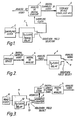
- an analogue video signal is fed to an analogue-to-digital converter controlled by a sampling clock 2 via a switching circuit 3 comprising two branches, in one of which a delay equal to half the clock period is arranged.
- a selector switching between the branches is controlled by the field synchronisation pulse element of the video signal so as to switch from one branch to the other according to whether it is in an odd or an even field of the frame.
- the digital sampled video signal is sent to a storage device 4 which may be a RAM or CCD, for example. For a two field interlaced frame system, sampling of alternate fields is 180° out of phase.
- Figures 2 and 3 show alternative embodiments of the read out stages of the device.
- the digital sampled video signal is read out of the storage device 4 and is passed to a digital-to-analogue converter 5, in which the signal is reconverted to analogue video.
- This signal then passes through a selective delay stage 6 comprising two branches, one of which contains a delay equivalent to the half clock period of the original sampling clock.
- a selector 8 switches between the two branches according to the field synchronisation pulse.
- a delay is introduced so that the pixels in the two frames of the resulting video frame are spatially aligned.
- an address counter 9 controls output from the storage device 4, which is a RAM.
- the address counter is controlled by a read clock 10 via a selective delay arrangement comprising two branches in one of which is a half clock period delay 12.
- a selector 13 selects between the two branches according the field to be selected.
- the digital data output from the RAM 4 is converted in a digital-to-analogue converter 5 and output as analogue video.
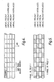
- Figure 4 illustrates the pixel distribution which would be generated by such a device on a standard monitor.
- the method of the invention has two advantages. Firstly the horizontal spatial resolution is increased, as the nyquist frequency has effectively been doubled.
- the second advantage is a reduction in aliasing. Previously, video information at frequencies higher than half sampling rate would be aliased back into the pass band as an additional noise component of the sampled signal. With the higher effective sampling rates afforded by the method of the invention, the effect of aliasing will be considerably reduced.
Landscapes
- Engineering & Computer Science (AREA)
- Multimedia (AREA)
- Signal Processing (AREA)
- Health & Medical Sciences (AREA)
- Toxicology (AREA)
- Television Systems (AREA)
- Transforming Light Signals Into Electric Signals (AREA)
- Closed-Circuit Television Systems (AREA)
Applications Claiming Priority (2)
| Application Number | Priority Date | Filing Date | Title |
|---|---|---|---|
| GB8914226 | 1989-06-21 | ||
| GB8914226A GB2233528B (en) | 1989-06-21 | 1989-06-21 | Thermal imaging system |
Publications (2)
| Publication Number | Publication Date |
|---|---|
| EP0404486A2 true EP0404486A2 (de) | 1990-12-27 |
| EP0404486A3 EP0404486A3 (de) | 1991-04-03 |
Family
ID=10658800
Family Applications (1)
| Application Number | Title | Priority Date | Filing Date |
|---|---|---|---|
| EP19900306627 Withdrawn EP0404486A3 (de) | 1989-06-21 | 1990-06-18 | Wärmebildsystem |
Country Status (2)
| Country | Link |
|---|---|
| EP (1) | EP0404486A3 (de) |
| GB (1) | GB2233528B (de) |
Cited By (1)
| Publication number | Priority date | Publication date | Assignee | Title |
|---|---|---|---|---|
| WO1995031064A1 (en) * | 1994-05-05 | 1995-11-16 | Imperial Chemical Industries | Thermal transfer printing |
Family Cites Families (11)
| Publication number | Priority date | Publication date | Assignee | Title |
|---|---|---|---|---|
| DE1903964B2 (de) * | 1969-01-28 | 1976-09-30 | Licentia Patent-Verwaltungs-Gmbh, 6000 Frankfurt | Digitales verfahren zum abtasten eines bildhaft darstellbaren geschehens oder symbols |
| DE2461719A1 (de) * | 1974-01-03 | 1975-07-10 | Emi Ltd | Datenanzeigeeinrichtung |
| US4068265A (en) * | 1974-11-25 | 1978-01-10 | Eli S. Jacobs | Method and apparatus for sampling and reproducing television information |
| DE2843232A1 (de) * | 1978-10-04 | 1980-04-17 | Bosch Gmbh Robert | Verfahren zur erzeugung von waermebildern |
| JPS58137377A (ja) * | 1982-02-09 | 1983-08-15 | Victor Co Of Japan Ltd | デイジタルビデオ信号伝送装置 |
| US4771275A (en) * | 1983-11-16 | 1988-09-13 | Eugene Sanders | Method and apparatus for assigning color values to bit map memory display locations |
| DE3437210A1 (de) * | 1984-10-10 | 1986-05-15 | Arnold & Richter Cine Technik GmbH & Co Betriebs KG, 8000 München | Anordnung zur verbesserung eines videosignals |
| JPS61253993A (ja) * | 1985-05-07 | 1986-11-11 | Nippon Hoso Kyokai <Nhk> | 立体テレビジョン画像信号の伝送方法 |
| GB8616616D0 (en) * | 1986-07-08 | 1986-08-13 | Philips Nv | Transmission system |
| FR2613166B1 (fr) * | 1987-03-24 | 1989-06-23 | Labo Electronique Physique | Dispositif de transmission d'images a haute definition par un canal a bande passante relativement etroite |
| JPS63245085A (ja) * | 1987-03-31 | 1988-10-12 | Pioneer Electronic Corp | サブサンプル内挿方法 |
-
1989
- 1989-06-21 GB GB8914226A patent/GB2233528B/en not_active Expired - Fee Related
-
1990
- 1990-06-18 EP EP19900306627 patent/EP0404486A3/de not_active Withdrawn
Cited By (1)
| Publication number | Priority date | Publication date | Assignee | Title |
|---|---|---|---|---|
| WO1995031064A1 (en) * | 1994-05-05 | 1995-11-16 | Imperial Chemical Industries | Thermal transfer printing |
Also Published As
| Publication number | Publication date |
|---|---|
| EP0404486A3 (de) | 1991-04-03 |
| GB8914226D0 (en) | 1989-12-28 |
| GB2233528A (en) | 1991-01-09 |
| GB2233528B (en) | 1994-01-05 |
Similar Documents
| Publication | Publication Date | Title |
|---|---|---|
| JP2673386B2 (ja) | 映像表示装置 | |
| US5977989A (en) | Method and apparatus for synchronizing video and graphics data in a multimedia display system including a shared frame buffer | |
| KR100414159B1 (ko) | 다채널 입력의 고화질 다중 화면 분할 장치 및 방법 | |
| NL8204684A (nl) | Met interlinieringsvrije dubbelaftasting werkend televisietoestel. | |
| JPH06217229A (ja) | 高画質tvのピクチャインピクチャ信号処理方法及びその装置 | |
| US5130814A (en) | Video recording and reproducing apparatus including dual offset ccd image arrays | |
| MY110080A (en) | Video memory system with double multiplexing of video and motion samples in a field memory for motion adaptivecompensation of processed video signals. | |
| US5381182A (en) | Flat panel image reconstruction interface for producing a non-interlaced video signal | |
| US5168359A (en) | Video scan rate conversion method and apparatus for achieving same | |
| EP0270269A2 (de) | Bildabtastverfahren | |
| EP0404486A2 (de) | Wärmebildsystem | |
| KR100420744B1 (ko) | 라인수변환방법및화상디스플레이장치 | |
| US4644398A (en) | Superinterlacing imaging systems | |
| EP0395429B1 (de) | Bildwiedergabevorrichtung | |
| EP0762737A2 (de) | Verbesserungen bei Anzeigevorrichtungen | |
| KR0123769B1 (ko) | 16 : 9 화면에서의 픽쳐 인 픽쳐 표시회로 | |
| JP3612760B2 (ja) | 映像信号処理方法 | |
| JPH0683419B2 (ja) | テレビジョン信号受信装置 | |
| JPH06311426A (ja) | 画像処理装置 | |
| JP2839061B2 (ja) | 画像処理装置 | |
| JPH0693774B2 (ja) | 走査線数の縮小方法 | |
| EP0762749A2 (de) | System zum Verarbeiten eines Videosignals für ein Videoanzeigesystem | |
| JPS63307698A (ja) | X線診断装置 | |
| JPS5952971A (ja) | テレビジヨン信号処理方式 | |
| JPH0744685B2 (ja) | Cctv監視システム |
Legal Events
| Date | Code | Title | Description |
|---|---|---|---|
| PUAI | Public reference made under article 153(3) epc to a published international application that has entered the european phase |
Free format text: ORIGINAL CODE: 0009012 |
|
| AK | Designated contracting states |
Kind code of ref document: A2 Designated state(s): DE FR IT NL |
|
| PUAL | Search report despatched |
Free format text: ORIGINAL CODE: 0009013 |
|
| AK | Designated contracting states |
Kind code of ref document: A3 Designated state(s): DE FR IT NL |
|
| 17P | Request for examination filed |
Effective date: 19910702 |
|
| 17Q | First examination report despatched |
Effective date: 19930820 |
|
| STAA | Information on the status of an ep patent application or granted ep patent |
Free format text: STATUS: THE APPLICATION IS DEEMED TO BE WITHDRAWN |
|
| 18D | Application deemed to be withdrawn |
Effective date: 19931231 |