EP0403992A2 - Chip-Trägergehäuse und Verfahren zur Herstellung - Google Patents
Chip-Trägergehäuse und Verfahren zur Herstellung Download PDFInfo
- Publication number
- EP0403992A2 EP0403992A2 EP90111407A EP90111407A EP0403992A2 EP 0403992 A2 EP0403992 A2 EP 0403992A2 EP 90111407 A EP90111407 A EP 90111407A EP 90111407 A EP90111407 A EP 90111407A EP 0403992 A2 EP0403992 A2 EP 0403992A2
- Authority
- EP
- European Patent Office
- Prior art keywords
- electrical conductors
- layer
- electrical
- mils
- chip carrier
- Prior art date
- Legal status (The legal status is an assumption and is not a legal conclusion. Google has not performed a legal analysis and makes no representation as to the accuracy of the status listed.)
- Withdrawn
Links
Images
Classifications
-
- H—ELECTRICITY
- H10—SEMICONDUCTOR DEVICES; ELECTRIC SOLID-STATE DEVICES NOT OTHERWISE PROVIDED FOR
- H10W—GENERIC PACKAGES, INTERCONNECTIONS, CONNECTORS OR OTHER CONSTRUCTIONAL DETAILS OF DEVICES COVERED BY CLASS H10
- H10W70/00—Package substrates; Interposers; Redistribution layers [RDL]
- H10W70/01—Manufacture or treatment
- H10W70/05—Manufacture or treatment of insulating or insulated package substrates, or of interposers, or of redistribution layers
-
- H—ELECTRICITY
- H10—SEMICONDUCTOR DEVICES; ELECTRIC SOLID-STATE DEVICES NOT OTHERWISE PROVIDED FOR
- H10W—GENERIC PACKAGES, INTERCONNECTIONS, CONNECTORS OR OTHER CONSTRUCTIONAL DETAILS OF DEVICES COVERED BY CLASS H10
- H10W70/00—Package substrates; Interposers; Redistribution layers [RDL]
- H10W70/60—Insulating or insulated package substrates; Interposers; Redistribution layers
- H10W70/67—Insulating or insulated package substrates; Interposers; Redistribution layers characterised by their insulating layers or insulating parts
- H10W70/68—Shapes or dispositions thereof
- H10W70/685—Shapes or dispositions thereof comprising multiple insulating layers
-
- Y—GENERAL TAGGING OF NEW TECHNOLOGICAL DEVELOPMENTS; GENERAL TAGGING OF CROSS-SECTIONAL TECHNOLOGIES SPANNING OVER SEVERAL SECTIONS OF THE IPC; TECHNICAL SUBJECTS COVERED BY FORMER USPC CROSS-REFERENCE ART COLLECTIONS [XRACs] AND DIGESTS
- Y10—TECHNICAL SUBJECTS COVERED BY FORMER USPC
- Y10T—TECHNICAL SUBJECTS COVERED BY FORMER US CLASSIFICATION
- Y10T29/00—Metal working
- Y10T29/49—Method of mechanical manufacture
- Y10T29/49002—Electrical device making
- Y10T29/49117—Conductor or circuit manufacturing
- Y10T29/49124—On flat or curved insulated base, e.g., printed circuit, etc.
- Y10T29/4913—Assembling to base an electrical component, e.g., capacitor, etc.
- Y10T29/49139—Assembling to base an electrical component, e.g., capacitor, etc. by inserting component lead or terminal into base aperture
- Y10T29/4914—Assembling to base an electrical component, e.g., capacitor, etc. by inserting component lead or terminal into base aperture with deforming of lead or terminal
-
- Y—GENERAL TAGGING OF NEW TECHNOLOGICAL DEVELOPMENTS; GENERAL TAGGING OF CROSS-SECTIONAL TECHNOLOGIES SPANNING OVER SEVERAL SECTIONS OF THE IPC; TECHNICAL SUBJECTS COVERED BY FORMER USPC CROSS-REFERENCE ART COLLECTIONS [XRACs] AND DIGESTS
- Y10—TECHNICAL SUBJECTS COVERED BY FORMER USPC
- Y10T—TECHNICAL SUBJECTS COVERED BY FORMER US CLASSIFICATION
- Y10T29/00—Metal working
- Y10T29/49—Method of mechanical manufacture
- Y10T29/49002—Electrical device making
- Y10T29/49117—Conductor or circuit manufacturing
- Y10T29/49124—On flat or curved insulated base, e.g., printed circuit, etc.
- Y10T29/49147—Assembling terminal to base
- Y10T29/49151—Assembling terminal to base by deforming or shaping
-
- Y—GENERAL TAGGING OF NEW TECHNOLOGICAL DEVELOPMENTS; GENERAL TAGGING OF CROSS-SECTIONAL TECHNOLOGIES SPANNING OVER SEVERAL SECTIONS OF THE IPC; TECHNICAL SUBJECTS COVERED BY FORMER USPC CROSS-REFERENCE ART COLLECTIONS [XRACs] AND DIGESTS
- Y10—TECHNICAL SUBJECTS COVERED BY FORMER USPC
- Y10T—TECHNICAL SUBJECTS COVERED BY FORMER US CLASSIFICATION
- Y10T29/00—Metal working
- Y10T29/49—Method of mechanical manufacture
- Y10T29/49002—Electrical device making
- Y10T29/49117—Conductor or circuit manufacturing
- Y10T29/49169—Assembling electrical component directly to terminal or elongated conductor
Definitions
- the present invention is directed to a novel chip carrier package and an improved method for interconnecting conductive layers in a chip carrier package.
- circuit boards which are used in relatively complicated pieces of equipment such as main frame computers, must be of a relatively high standard of quality in order to function in an efficient manner for a long period of time without deteriorating or breaking down, and thus causing an interruption in the function of the machine.
- This high quality of material and design is opposed to pieces of equipment requiring a lower standard of quality such as those used in personal computers, high quality television equipment, radios etc.
- Circuit boards are prepared by laminating conducting sheets, e.g. copper sheets, with sheets of electrical insulating materials, such as glass fiber reinforced polyester resin sheets or nonreinforced polyimides.
- electrical circuit boards may be either rigid or flexible, and are further classified as single-sided (metal foil on one side of the insulating material only), double-sided (metal foil on both sides of the insulating material), or multilayered. Further for those circuit boards which are multilayered, the conductive layers within the package must be interconnected, for example with plated through holes as well as interconnected to other circuit boards or electrical components. Further still, there are multilayered circuit boards which contain a semiconductor chip, called chip carrier packages.
- U.S. Patent 4,517,050 discloses the method by which a conductive through-hole hole is formed through a dielectric sandwiched between conductors by forming a noncircular hole in a conductor, etching a hole through the dielectric and by deforming the conductor which has been undercut during the etching.
- This method does not permit for high dense packing of lines, as the holes formed in the conductive layer and the annular ring of conductor around such holes take up space needed for the circuit lines. This method can take up 22.5 mils on the conductive layer for interconnection purposes.
- U.S. Patent 3,969,815 discloses a process for providing electrical interconnection of two metal layers positioned on opposite sides of a substrate.
- a hole is initially drilled or bored completely through the two metal layers and the intermediate insulating layer.
- the hole in the insulating layer is enlarged by a selective etching process which only etches the insulating layer to form an enlarged annular hole in the insulating layer which undercuts the metal layer portions.
- These overhanging metal portions on opposite sides of the insulating layer are deformed by pressure to contact or almost contact one another.
- the deformed metal portions are coated by galvanic metal which is overcoated by a thin layer, preferably tin, to form a conductive path. This process requires much tooling and set up work for the manufacture of the circuit board.
- a further object of this invention is to provide a method of interconnecting conductive layers in which circuit line densities on a conductive layer are not limited by the interconnection between the conductive layers. Interconnection of circuit lines from layer to layer, as taught by prior art methods, consumes much space on the layer thus reducing the amount of space available for circuit lines. Distances between circuit line centers can be as small as 6 mil in this invention, so that the density of circuit lines on a layer is increased.
- Another object of this invention is to provide a method of interconnecting conductive layers at the inner and/or outer edges of the conductive layers of a chip carrier package.
- Many prior art methods teach interconnection of conductive layers interior to an electrical package.
- Another object of this invention is to provide for an electrical multilayer conductive package which partitions the power supply system of the package from the signal transmission system as much as practical in order to optimize the performance of both.
- Still another object of the invention is to provide for an electrical multiconductive layer package in which the interconnection from a first conductive layer to a second conductive layer is flexible and yet very reliable so that the total package has excellent resistance to failure from thermal cycling mechanical stress.
- the present invention is directed to a chip carrier package comprising
- the present invention is particularly adapted for forming interconnections between conductive layers separated by dielectric layers in a chip carrier package. More particularly, the present invention relates to the formation of an unsupported terminus of the circuit lines on an uppermost conductive layer and the subsequent interconnection of the unsupported terminus to bonding pads sites located on an adjacent conductive layer below.
- a laminate of an electrically conductive composite consisting of a metal conductive layer and a dielectric layer with for example an adhesive layer therebetween, are conventional starting materials for forming multilayer boards such as chip carrier packages and are suitable herein.
- the dielectric layer will be at least one mil in thickness and the conductive layer will be 0.7 to 2.8 mils thick, e.g., copper foil, although both thinner and thicker layers can be used.
- the materials of construction of the dielectric insulating layer are not critical except that they have the appropriate electrical properties and can be etched using plasma, chemical or laser etching.
- dielectric layer examples include polyimide thermosetting resin polymers, and perfluorinated polymers, such as polytetrafluoroethylene (TFE), copolymers of tetrafluoroethylene and hexafluoropropylene and copolymers of tetrafluoroethylene and perfluoro(propyl vinyl ether) and the like.
- TFE polytetrafluoroethylene
- dielectric materials which are supported such as polyaramids in either form of woven or nonwoven fabric such as made from continuous fibers are suitable in this invention so long as the support can also be etched.
- Metals suitable for the metal conductive layer include copper, silver and gold, with copper being preferred.
- a particularly preferred laminate is a copper clad polyimide film.
- circuit lines for the package application On each of the conductive layers the desired circuit patterns are formed of circuit lines for the package application. This includes the conductive layer which uppermost on the package and which has the terminus of circuit lines for attachment to an adjacent conductive layer.
- the circuit lines are signal lines, but they can be ground or power lines or pads.
- the circuit lines are formed preferably by chemical etching which is well known in the formation of printed circuits.
- An example of such chemical etching involves lamination of a negative acting photosensitive film, for example Riston® 218R photoresist to the conductor surface which does not face the dielectric layer, exposing the photosensitive polymer to actinic radiation through a photomask, developing and removing unexposed photosensitive polymer to expose portions of the metal layer and thereafter chemically etching completely through the thickness of the exposed conductive layer.
- the chemical etching step removes little or no material from the dielectric polymer layer.
- a suitable process is disclosed in Celeste U.S. Patent No. 3,469,982. Positive working photopolymers with processing techniques well known in the art can likewise be used, e.g., Cohen and Heiart U.S. Patent No. 4,193,797.
- the formation of the terminus of the circuit lines for the uppermost conductive layer on the circuit side of a metal, adhesive, dielectric laminate structure is accomplished by conventional etching methods.
- a metal mask is placed over the dielectric layer of the laminate structure so that various circuit lines having a longer length extend into the center of an etched pattern of signal lines and power and ground lines or pads on the conductive layer where a chip cavity will eventually exist.
- the laminate structure with mask so positioned is then etched to undercut and remove the dielectric underlayer of the metal circuit lines extending into cavity area. This etching step also forms a central cavity as the dielectric is completely removed and no metal, other than that of the extended circuit lines remains in the area.
- An example of an etching technique which etches completely through the dielectric layer and laterally to undercut the conductive layer and is suitable herein is liquid chemical etching.
- the etching technique used is dependent upon the type of dielectric material to be removed by the etching process. Particularly preferred method is liquid chemical etching.
- Liquid etching techniques by which a liquid can etch selectively through a polymeric dielectric are well-known in the art.
- the etchant will not cause a substantial removal of the conductive material.
- Suitable etchants include those disclosed in U.S. Patent 3,969,815, and Kreuz and Hawkins U.S. Patent 4,426,253, e.g.
- a sulfuric acid solution can be used for polyester and epoxide resins while a caustic alcoholic solution is suitable for a polyimide.
- etching includes use of solvents capable of removing areas of the dielectric not masked by the conductive matal without any deleterious effect on the metal may be used. Examples of solvents are tetrachloroethylene, methyl chloroform, mixture of 90% tetrachloroethylene and 10% isobutyl alcohol (by volume) and chromic acid.
- etching techniques which etch completely through the dielectric layer are laser etching and plasma etching.
- This method uses an excimer laser, which produces ultraviolet light.
- Factors which control the capability and efficiency of the laser are the energy density of the laser pulse, the ablation rate which is the etch depth in the dielectric per pulse and the pulse power.
- Suitable setting for laser etching a polyimide are 800 to 900 millijoules/cm2 for energy density, ablation rate of 0.2 microns/pulse, and average pulse power of 200 millijoules per pulse.
- the dielectric is ablated by the laser by either a step and repeat or a scan area method. Frequently a char residue remains where the laser has etched the dielectric. The char residue is easily removed by various techniques. In plasma etching technique however, a separate metal mask with the window cut out where the cavity will be is placed on the dielectric layer of the uppermost conductive layer. Also during plasma etching, the lines of the circuit pattern on the metal conductive layer can be appropriately formed to serve as a mask for the dielectric since the plasma attacks the dielectric where the dielectric layer is not protected by the metal pattern or mask. The metal is substantially unaffected by the plasma or, at least, the etching rate of the dielectric is considerably faster than the etching rate of the conductor.
- etching gas is chosen so as to produce species which react chemically with the material to be etched to form a reaction product which is volatile. Mixtures of various plasma gases can also be used.
- a preferred gas composition to be used where the dielectric is a polyimide and the mask is copper is carbon tetrafluoride/oxygen in the ratio of 50/50 to 10/90 by volume.
- the interconnection does not limit the circuit line densities on the conductive layer. Rather the limitations are those of the photoresist to resolve the lines, the tensile strength of the metal and the ability to plate down the extended lines of the uppermost conductive layer.
- the circuit lines on a conductive layer which is to interconnect with another conductive layer, can have as close as 6 mil and less centers, i.e., a center of an electrical conductor is spaced 6 mils from a center of an adjacent conductor, such as 3 mil wide spaces between circuit lines of 3 mil width. Spacing of conductors of 8, 10, or 12 mils can be easily accomplished.
- the uppermost layer with the unsupported terminus of circuit lines extending into the opening or cavity is attached to the package base such that a shelf which is of a wall construction which can be sloping or at right angles is formed on the top conductive layer of the package base. Attachment of the uppermost layer to the top of the package base, is accomplished by laminating in register, as is well known in the art, with an adhesive layer between the two layers. Thereafter, the extending circuit lines are deformed to come in mating contact with the bonding pads exposed on the shelf of the top conductive layer on the package base. Methods which are suitable for deforming metal lines are by mechanical means or by ultrasonic bonding which are well known to those skilled in the art. Mechanical deformation of the extending metal lines can occur in a laminating press. An instrument suitable for ultrasonic deformation of the extending metal lines is manufactures by Kulick & Soffa, described as a heavy gauge ultrasonic wedge bonder, model number 4127.
- the deformed electrically conductive mterial may be electrolytically plated with a metal such as copper, electrolessly plated or soldered or welded to complete or ensure an electrically conductive path.
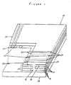
- a chip carrier package comprising of a base (12) with 4 layers of conductive planes (14) which are used as power and ground pathways in the package (10). Underneath between each plane (14) is a dielectric layer (16). The conductive paths used for power and ground for the package (10) are interconnected by means of a series of interconnecting vias (15) formed through the dielectric layers (16) interposed between each plane (14) to paths that are on the top plane layer (18) of the base (12). Selective paths on the top plane layer (18) centrally terminate to contact pads (19).
- the base (12) is a dielectric layer and a circuit layer which has a plurality of signal lines (24), and bonding pads (25) for connecting the chip to power and ground layers buried within the package, called the signal layer (20).
- the signal layer (20) of the package (10) is positioned such that the top plane layer (18) of the base (12) forms a shelf (22) extending out from under the signal layer (20) thereby exposing selective contact pads (19).
- the terminus (23) of the ground and power pads (25) on the signal layer (20) extend over the cavity formed in the dielectric layer under the signal layer (20) and are deformed to connect in a mating fashion to the exposed contact pads (19) on the shelf (22) of the top plane layer (18) of the base (12).
- the side of the base (12) opposite the signal layer (20) is affixed to a body of metal (26).
- a cavity (28) extends through all of the base (12) forming side walls (30) and signal (20) layers and has as its support the body of metal (26).
- the package is completed for use by mounting a semiconductor chip on the body of metal (26) and connecting the chip with conductors to the signal circuit lines and to the bonding pads (25) that connect the ground and power paths to the power and ground paths buried within the package.
- a sandwich was created of first the flexible circuit material with the newly formed circuit pattern, a Pyralux® WA 1 mil adhesive layer on top of this first layer, and a new piece of Pyralux® flexible circuit laminate on top of the adhesive layer.
- the sandwich was permanently bonded to a metal substrate, for example an aluminum sheet, by contacting the bottom of the first layer, i.e., the dielectric, to the metal substrate with a 1 mil layer of Pyralux® WA adhesive.
- the first and second plane layers were attached to the metal substrate.
- Via windows with extended “tabs” were formed in the top copper layer cover (which is the second layer of the flexible circuit laminate) by using known art of photoresists and copper etching as disclosed in U.S. Patent 4,517,050.
- the dielectric layer under the via window "tabs” was removed by using a CO2 laser (manufactured by Coherent General Corp.) followed by plasma etching the sandwich in a carbon tetrafluoride and oxygen mixture for 5 to 15 minutes.
- the via window "tabs” were deformed mechanically to mate with the corresponding pads formed in the layer below (first layer) (as described in the above cited patents).
- a photoresist layer was applied to the top copper layer (second layer), then image-wise exposed through a photomask, to form the circuit lines and ground planes on the second layer.
- the deformed tabs were plated with copper (using an acid copper bath) and then solder (as an etch resist) to their corresponding pad below to make a permanent electrical contact.
- the photoresist layer was removed and all excess or background copper from the imaged pattern was etched away (using an ammoniacal etchant). Finally the solder etch resist was stripped.
- the sandwich was cleaned and baked to prepare for the next layer of flexible circuit composite.
- the next layer (third layer) of the flexible circuit composite was laminated to the previously prepared layer with an adhesive layer therebetween.
- the sandwich was cleaned and baked to prepare for the next layer of flexible circuit composite.
- the next layer (fourth layer) of the flexible circuit composite was laminated to the previously prepared layer with an adhesive layer therebetween.
- the uppermost layer was prepared by etching the signal lines as described previously a new piece of Pyralux® flexible circuit laminate.
- a window with certain leads extending into its open space was formed in the center of the signal layer flexible circuit using an aluminum mask with a cut out for the window was placed directly over the area to be etched on the adhesive side of the circuit and a sheet of aluminum protecting the signal side.
- An adhesive layer with white paper backing and a window in the center to correspond to aluminum mask was fashioned by a punch and die, and tack laminated to the polyimide side of the signal layer.
- the paper used for this purpose was that found on the Pyralux® WA adhesive.
- the signal layer was plasma etched with the paper removed after plasma etching.
- the signal layer was temporarily affixed to the top layer (fourth layer) of the base element.
- the signal layer was positioned such that a shelf was formed by the fourth layer containing the contact pads was exposed.
- Registered holes were formed in the signal layer and the base element using a programmed drill. Pins were inserted into the holes.
- the uppermost signal layer and the base element were laminated together so as to cause the adhesive tacked to the signal layer to bond to the base element and permanently cure while maintaining registration with the bottom layer.
- the registration pins were removed.
- the lines for power and ground distribution of the uppermost signal layer which extend into the window were deformed to mate with a corresponding contact pad residing on the shelf of the base element.
- the extended lines were deformed by mechanical means.
- the press was pressurized to 1000 psi to collapse the extended lines onto the contact pads on the shelf.
- the deformed lines were plated with their mating circuit lines to form a continuous permanent bonded line thus establishing an interconnection from the uppermost signal layer to the layer just below.
- a cavity from the window edge to the top of the metal support was routed by means of a numerically controlled router into the layers of the base element.
Landscapes
- Production Of Multi-Layered Print Wiring Board (AREA)
- Lead Frames For Integrated Circuits (AREA)
- Wire Bonding (AREA)
Applications Claiming Priority (2)
| Application Number | Priority Date | Filing Date | Title |
|---|---|---|---|
| US368481 | 1989-06-19 | ||
| US07/368,481 US4965702A (en) | 1989-06-19 | 1989-06-19 | Chip carrier package and method of manufacture |
Publications (2)
| Publication Number | Publication Date |
|---|---|
| EP0403992A2 true EP0403992A2 (de) | 1990-12-27 |
| EP0403992A3 EP0403992A3 (de) | 1992-12-30 |
Family
ID=23451402
Family Applications (1)
| Application Number | Title | Priority Date | Filing Date |
|---|---|---|---|
| EP19900111407 Withdrawn EP0403992A3 (de) | 1989-06-19 | 1990-06-16 | Chip-Trägergehäuse und Verfahren zur Herstellung |
Country Status (3)
| Country | Link |
|---|---|
| US (1) | US4965702A (de) |
| EP (1) | EP0403992A3 (de) |
| JP (1) | JPH03174742A (de) |
Cited By (2)
| Publication number | Priority date | Publication date | Assignee | Title |
|---|---|---|---|---|
| EP0571907A3 (de) * | 1992-05-29 | 1994-02-16 | Eastman Kodak Co | |
| WO1996004681A1 (en) * | 1994-07-29 | 1996-02-15 | Havant International Limited | Direct chip attach |
Families Citing this family (36)
| Publication number | Priority date | Publication date | Assignee | Title |
|---|---|---|---|---|
| US5299730A (en) * | 1989-08-28 | 1994-04-05 | Lsi Logic Corporation | Method and apparatus for isolation of flux materials in flip-chip manufacturing |
| US5236551A (en) * | 1990-05-10 | 1993-08-17 | Microelectronics And Computer Technology Corporation | Rework of polymeric dielectric electrical interconnect by laser photoablation |
| DE59105080D1 (de) * | 1990-05-28 | 1995-05-11 | Siemens Ag | IC-Gehäuse, bestehend aus drei beschichteten dielektrischen Platten. |
| US5280414A (en) * | 1990-06-11 | 1994-01-18 | International Business Machines Corp. | Au-Sn transient liquid bonding in high performance laminates |
| US5399903A (en) * | 1990-08-15 | 1995-03-21 | Lsi Logic Corporation | Semiconductor device having an universal die size inner lead layout |
| US5117275A (en) * | 1990-10-24 | 1992-05-26 | International Business Machines Corporation | Electronic substrate multiple location conductor attachment technology |
| DE69210329T2 (de) * | 1991-07-25 | 1996-11-28 | Ncr Int Inc | Mehrschichtiger Träger für integrierte Schaltungen und Verfahren zu dessen Herstellung |
| US5210683A (en) * | 1991-08-22 | 1993-05-11 | Lsi Logic Corporation | Recessed chip capacitor wells with cleaning channels on integrated circuit packages |
| US5249098A (en) * | 1991-08-22 | 1993-09-28 | Lsi Logic Corporation | Semiconductor device package with solder bump electrical connections on an external surface of the package |
| US5434750A (en) * | 1992-02-07 | 1995-07-18 | Lsi Logic Corporation | Partially-molded, PCB chip carrier package for certain non-square die shapes |
| JP2554542Y2 (ja) * | 1992-02-17 | 1997-11-17 | 台灣杜邦股▲ふん▼有限公司 | プリント回路基板 |
| US5854085A (en) * | 1992-06-04 | 1998-12-29 | Lsi Logic Corporation | Multi-layer tab tape having distinct signal, power and ground planes, semiconductor device assembly employing same, apparatus for and method of assembling same |
| JPH0653277A (ja) * | 1992-06-04 | 1994-02-25 | Lsi Logic Corp | 半導体装置アセンブリおよびその組立方法 |
| US5801432A (en) * | 1992-06-04 | 1998-09-01 | Lsi Logic Corporation | Electronic system using multi-layer tab tape semiconductor device having distinct signal, power and ground planes |
| US5854534A (en) * | 1992-08-05 | 1998-12-29 | Fujitsu Limited | Controlled impedence interposer substrate |
| US5294567A (en) * | 1993-01-08 | 1994-03-15 | E. I. Du Pont De Nemours And Company | Method for forming via holes in multilayer circuits |
| US5419038A (en) * | 1993-06-17 | 1995-05-30 | Fujitsu Limited | Method for fabricating thin-film interconnector |
| US5438477A (en) * | 1993-08-12 | 1995-08-01 | Lsi Logic Corporation | Die-attach technique for flip-chip style mounting of semiconductor dies |
| US5388327A (en) * | 1993-09-15 | 1995-02-14 | Lsi Logic Corporation | Fabrication of a dissolvable film carrier containing conductive bump contacts for placement on a semiconductor device package |
| US5391914A (en) * | 1994-03-16 | 1995-02-21 | The United States Of America As Represented By The Secretary Of The Navy | Diamond multilayer multichip module substrate |
| US6025256A (en) * | 1997-01-06 | 2000-02-15 | Electro Scientific Industries, Inc. | Laser based method and system for integrated circuit repair or reconfiguration |
| US5798563A (en) * | 1997-01-28 | 1998-08-25 | International Business Machines Corporation | Polytetrafluoroethylene thin film chip carrier |
| US6057594A (en) * | 1997-04-23 | 2000-05-02 | Lsi Logic Corporation | High power dissipating tape ball grid array package |
| US6639155B1 (en) | 1997-06-11 | 2003-10-28 | International Business Machines Corporation | High performance packaging platform and method of making same |
| JP2950290B2 (ja) * | 1997-06-27 | 1999-09-20 | 日本電気株式会社 | 高周波集積回路装置およびその製造方法 |
| JP3579740B2 (ja) * | 1998-04-18 | 2004-10-20 | Tdk株式会社 | 電子部品の製造方法 |
| KR100335481B1 (ko) * | 1999-09-13 | 2002-05-04 | 김덕중 | 멀티 칩 패키지 구조의 전력소자 |
| US6431750B1 (en) | 1999-12-14 | 2002-08-13 | Sierra Lobo, Inc. | Flexible temperature sensing probe |
| TW434821B (en) * | 2000-02-03 | 2001-05-16 | United Microelectronics Corp | Allocation structure of via plug to connect different metal layers |
| US20030213619A1 (en) * | 2002-05-14 | 2003-11-20 | Denzene Quentin S. | Ground discontinuity improvement in RF device matching |
| US7196016B2 (en) * | 2003-09-29 | 2007-03-27 | Hitachi Global Storage Technologies Netherlands, B.V. | Fabrication process for preparing recording head sliders made from silicon substrates with SiO2 overcoats |
| FR2893448A1 (fr) * | 2005-11-15 | 2007-05-18 | St Microelectronics Sa | Dispositif semi-conducteur a plusieurs puces de circuits integres assemblees et procede d'assemblage et de connexion electrique de puces de circuits integres |
| JP5354380B2 (ja) * | 2007-03-30 | 2013-11-27 | 日本電気株式会社 | 電子機器の配線構造及び電子機器パッケージの製造方法 |
| US8072764B2 (en) * | 2009-03-09 | 2011-12-06 | Apple Inc. | Multi-part substrate assemblies for low profile portable electronic devices |
| US9320130B2 (en) * | 2010-10-25 | 2016-04-19 | Korea Electric Terminal Co., Ltd. | Printed circuit board, and board block for vehicles using the same |
| US11205530B1 (en) * | 2017-12-13 | 2021-12-21 | Triad National Security, Llc | Technique for constructing high gradient insulators |
Family Cites Families (5)
| Publication number | Priority date | Publication date | Assignee | Title |
|---|---|---|---|---|
| DE2347217A1 (de) * | 1973-09-19 | 1975-03-27 | Siemens Ag | Verfahren zum durchkontaktieren eines beidseitig metallkaschierten basismaterials fuer gedruckte schaltungen |
| FR2439322A1 (fr) * | 1978-10-19 | 1980-05-16 | Cii Honeywell Bull | Procede et dispositif de liaison de deux elements et outil pour l'execution du procede |
| US4608592A (en) * | 1982-07-09 | 1986-08-26 | Nec Corporation | Semiconductor device provided with a package for a semiconductor element having a plurality of electrodes to be applied with substantially same voltage |
| US4630172A (en) * | 1983-03-09 | 1986-12-16 | Printed Circuits International | Semiconductor chip carrier package with a heat sink |
| US4517050A (en) * | 1983-12-05 | 1985-05-14 | E. I. Du Pont De Nemours And Company | Process for forming conductive through-holes through a dielectric layer |
-
1989
- 1989-06-19 US US07/368,481 patent/US4965702A/en not_active Expired - Fee Related
-
1990
- 1990-06-16 EP EP19900111407 patent/EP0403992A3/de not_active Withdrawn
- 1990-06-19 JP JP2158886A patent/JPH03174742A/ja active Pending
Cited By (2)
| Publication number | Priority date | Publication date | Assignee | Title |
|---|---|---|---|---|
| EP0571907A3 (de) * | 1992-05-29 | 1994-02-16 | Eastman Kodak Co | |
| WO1996004681A1 (en) * | 1994-07-29 | 1996-02-15 | Havant International Limited | Direct chip attach |
Also Published As
| Publication number | Publication date |
|---|---|
| EP0403992A3 (de) | 1992-12-30 |
| US4965702A (en) | 1990-10-23 |
| JPH03174742A (ja) | 1991-07-29 |
Similar Documents
| Publication | Publication Date | Title |
|---|---|---|
| US4965702A (en) | Chip carrier package and method of manufacture | |
| US5774340A (en) | Planar redistribution structure and printed wiring device | |
| US5685070A (en) | Method of making printed circuit board | |
| EP0843955B1 (de) | Verfahren zur herstellung von erhöhten metallischen kontakten auf elektrischen schaltungen | |
| EP0144944B1 (de) | Verfahren zur Herstellung von leitfähigen, durchgehenden Löchern durch eine dielektrische Schicht | |
| EP0545328B1 (de) | Herstellungsverfahren für eine gedruckte Schaltung | |
| EP0144943B1 (de) | Plasmaverfahren zur Herstellung leitfähiger durchgehender Löcher durch eine dielektrische Schicht | |
| EP0228694A2 (de) | Verfahren zur Herstellung von leitenden Durchführungen in einer dielektrischen Schicht unter Verwendung einer Kombination von Laserätzung und anderen Ätzmitteln | |
| US6956182B2 (en) | Method of forming an opening or cavity in a substrate for receiving an electronic component | |
| EP0146061B1 (de) | Flüssiges chemisches Verfahren zur Herstellung von leitfähigen durchgehenden Löchern durch eine dielektrische Schicht | |
| US6954986B2 (en) | Method for fabricating electrical connecting element | |
| US7288739B2 (en) | Method of forming an opening or cavity in a substrate for receiving an electronic component | |
| JPH01282892A (ja) | 多層印刷配線板の製造方法 | |
| JP3155565B2 (ja) | プリント配線板の製造方法 | |
| US6492007B1 (en) | Multi-layer printed circuit bare board enabling higher density wiring and a method of manufacturing the same | |
| US4769269A (en) | Article containing conductive through-holes | |
| JPH08307057A (ja) | 多層配線回路基板及びその製造方法 | |
| EP1259102B1 (de) | Unbestückte mehrschichtige Leiterplatte zum ermöglichen einer höheren Verdrahtungsdichte und Verfahren zu deren Herstellung | |
| JP2005108941A (ja) | 多層配線板及びその製造方法 | |
| JPS61284991A (ja) | アルミニウム/銅複合箔張基板の回路形成法 | |
| WO2001065595A2 (en) | A method of forming an opening or cavity in a substrate for receiving an electronic component | |
| EP1517599A1 (de) | Verfahren zur Verbindung der gegenüberliegenden Seiten einer Verbindungsanordnung für elektronische Bauteile | |
| JPH04314378A (ja) | 印刷配線板及びその製造法 | |
| JP2003007777A (ja) | フィルムキャリア及びその製造方法 | |
| JPH0817963A (ja) | Pga型パッケージおよびそのプリント配線板の製造方法 |
Legal Events
| Date | Code | Title | Description |
|---|---|---|---|
| PUAI | Public reference made under article 153(3) epc to a published international application that has entered the european phase |
Free format text: ORIGINAL CODE: 0009012 |
|
| AK | Designated contracting states |
Kind code of ref document: A2 Designated state(s): CH DE FR GB LI |
|
| 17P | Request for examination filed |
Effective date: 19901126 |
|
| PUAL | Search report despatched |
Free format text: ORIGINAL CODE: 0009013 |
|
| AK | Designated contracting states |
Kind code of ref document: A3 Designated state(s): CH DE FR GB LI |
|
| 17Q | First examination report despatched |
Effective date: 19931228 |
|
| STAA | Information on the status of an ep patent application or granted ep patent |
Free format text: STATUS: THE APPLICATION IS DEEMED TO BE WITHDRAWN |
|
| 18D | Application deemed to be withdrawn |
Effective date: 19940104 |