EP0403088A2 - Gleichstrom-Konverter - Google Patents
Gleichstrom-Konverter Download PDFInfo
- Publication number
- EP0403088A2 EP0403088A2 EP90305496A EP90305496A EP0403088A2 EP 0403088 A2 EP0403088 A2 EP 0403088A2 EP 90305496 A EP90305496 A EP 90305496A EP 90305496 A EP90305496 A EP 90305496A EP 0403088 A2 EP0403088 A2 EP 0403088A2
- Authority
- EP
- European Patent Office
- Prior art keywords
- gates
- converter
- output
- regulated
- power transistor
- Prior art date
- Legal status (The legal status is an assumption and is not a legal conclusion. Google has not performed a legal analysis and makes no representation as to the accuracy of the status listed.)
- Withdrawn
Links
Images

Classifications
-
- H—ELECTRICITY
- H02—GENERATION; CONVERSION OR DISTRIBUTION OF ELECTRIC POWER
- H02M—APPARATUS FOR CONVERSION BETWEEN AC AND AC, BETWEEN AC AND DC, OR BETWEEN DC AND DC, AND FOR USE WITH MAINS OR SIMILAR POWER SUPPLY SYSTEMS; CONVERSION OF DC OR AC INPUT POWER INTO SURGE OUTPUT POWER; CONTROL OR REGULATION THEREOF
- H02M3/00—Conversion of DC power input into DC power output
- H02M3/22—Conversion of DC power input into DC power output with intermediate conversion into AC
- H02M3/24—Conversion of DC power input into DC power output with intermediate conversion into AC by static converters
- H02M3/28—Conversion of DC power input into DC power output with intermediate conversion into AC by static converters using discharge tubes with control electrode or semiconductor devices with control electrode to produce the intermediate AC
- H02M3/325—Conversion of DC power input into DC power output with intermediate conversion into AC by static converters using discharge tubes with control electrode or semiconductor devices with control electrode to produce the intermediate AC using devices of a triode or a transistor type requiring continuous application of a control signal
- H02M3/335—Conversion of DC power input into DC power output with intermediate conversion into AC by static converters using discharge tubes with control electrode or semiconductor devices with control electrode to produce the intermediate AC using devices of a triode or a transistor type requiring continuous application of a control signal using semiconductor devices only
- H02M3/337—Conversion of DC power input into DC power output with intermediate conversion into AC by static converters using discharge tubes with control electrode or semiconductor devices with control electrode to produce the intermediate AC using devices of a triode or a transistor type requiring continuous application of a control signal using semiconductor devices only in push-pull configuration
- H02M3/3376—Conversion of DC power input into DC power output with intermediate conversion into AC by static converters using discharge tubes with control electrode or semiconductor devices with control electrode to produce the intermediate AC using devices of a triode or a transistor type requiring continuous application of a control signal using semiconductor devices only in push-pull configuration with automatic control of output voltage or current
- H02M3/3378—Conversion of DC power input into DC power output with intermediate conversion into AC by static converters using discharge tubes with control electrode or semiconductor devices with control electrode to produce the intermediate AC using devices of a triode or a transistor type requiring continuous application of a control signal using semiconductor devices only in push-pull configuration with automatic control of output voltage or current in a push-pull configuration of the parallel type
Definitions
- This invention relates to DC-DC converters and relates more particularly to such converters for providing regulated switch mode DC supplies preferably affording isolation between the power supplies and load circuits.
- the present invention is especially, but not exclusively, concerned with the provision of regulated switch mode isolated power supplies in circuits of the kind described in our co-pending Patent Application No. 8825438.8 (F20596).
- One primary objective of the invention is to provide DC-DC convertors of relatively simple and cheap construction affording switch mode regulation of the convertor output.
- a regulated switch mode DC-DC converter comprising a logic gate package connected to a DC power supply and providing four NOR logic gates, in which two of the NOR gates are connected for providing an oscillator circuit producing one or more AC outputs which are applied to the inputs of the other respective NOR gates which act as driver gates for power transistor means which conducts intermittently in order to provide from DC power supply regulated current which may be fed to the primary of a de-coupling or isolating transformer the secondary of which feeds a rectified circuit which provides a DC regulated output, and in which the ON/OFF periods of the power transistor means are controlled by control means in order to provide the requisite regulation of the DC output of the converter.
- the oscillator circuit may provide two AC outputs in anti-phase which are applied to the inputs of two NOR gates the outputs from which drive to power transistors which conduct alternately.
- Regulation of the DC-DC converter by controlling initiation of the switching points of the power transistors and thus the ON/OFF periods of the converter may be achieved by controlling the charge on capacitors connected to respective inputs of the NOR gates controlling the switching points of the power transistors.
- the present invention enables a standard volume-produced low- cost logic gate package to be used which effectively produces the requisite ON/OFF period or mark-space ratio and provides driver for the power transistor stage of the converter.
- the present invention avoids the use of high power loss linear regulators connected in series with unregulated DC-DC converters in order to achieve regulation.
- Known switch mode regulated power circuits are complex and expensive due to the use of specialised components and although high efficiencies are achieved on load, off-load losses may be too high for applications in which off-load losses are important.
- electrical isolation by the use of transformers is required the costs of the switch mode regulated DC-DC converter become even higher.
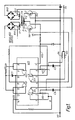
- the switch mode regulated DC-DC converter illustrated comprises a standard volume-produced relatively low cost logic circuit device LCD providing four NOR logic gates G1, G2, G3 and G4.
- the two NOR gates G1 and G2 are connected with a resistor R1 and capacitor C1 in order to provide an oscillator circuit having an operating frequency of between 10 to 500 KHz dependent upon the values of the resistor R1 and the capacitor C1.
- the two outputs from the oscillator circuit at points P and Q are of similar form but in anti-phase. These anti-phase outputs are applied directly to inputs X of respective NOR gates G3 and G4 and through resistors R2 and R3 to the other inputs Y of the two gates.
- the DC battery input to the converter to be regulated which may, in the case of aircraft power supplies vary between 16 to 32 volts, is applied to terminals VS and VO (e.g. earth ).
- the potential at terminal VO is applied to the logic circuit device LCD and the emitters of two power transistors TR1 and TR2 whilst the positive voltage at terminal VS is applied to the collectors of the transistors TR1 and TR2 through respective parts P1 and P2 of a centre-tapped primary winding P of an isolating transformer TX.
- the transformer TX has two isolated secondary windings S1 and S2 having full-wave rectifier circuits RX1 and RX2 connected there across.
- the DC output from the rectifier circuit RX2 comprises a feedback voltage and is applied through resistors R4 and R5 to capacitors C2 and C3, with a smoothing capacitor C4 being connected across the output.
- the DC output from the other rectifier RX1 constitutes the regulated output from the converter.
- the outputs Z from the NOR gates G3 and G4 are connected to the bases of the respective power transistors TR1 and TR2.
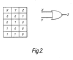
- the oscillator outputs P and Q will cause the logic inputs to the gates G3 and G4 to change from logic 1 to logic 0 and vice versa.
- the application of logic 1 or logic 0 signals to the inputs Y of the gates G3 and G4 will be delayed in dependence upon the charged state of the capacitors C2 and C3.
- the charged state of the capacitors C2 and C3 is in turn dependent upon the voltage V sand and the output voltage from the rectifier bridge RX2 and the load connected to the rectifier bridge RX1.
- the discharge time for the capacitors C2 and C3 when the oscillator outputs at P and Q are alternately logic 0 will depend upon the charged state of the capacitors C2 and C3.
- This discharge time determines when both of the inputs X and Y become logic 0 in order to produce a logic 1 output at outputs Z of the gates G3 and G4 so as to switch on the power transistors TR1 and TR2.
- the power transistors switch on alternately and, in so doing, the circuits for the energisation of the respective parts P1 and P2 of the transformer primary winding P of the isolating transformer TX are closed.
- this demonstrates how the mark-space ratios of the output voltage pulses from the gates G3 and G4 vary in dependence upon the load connected to the rectifier RX1 and the voltage VS (i.e. battery voltage).
- the diagram also shows how the collector currents (i1) and (i2) of the power transistors TR1 and TR2 vary with the load and voltage VS.
Landscapes
- Engineering & Computer Science (AREA)
- Power Engineering (AREA)
- Dc-Dc Converters (AREA)
Applications Claiming Priority (2)
| Application Number | Priority Date | Filing Date | Title |
|---|---|---|---|
| GB8913772A GB2232795B (en) | 1989-06-15 | 1989-06-15 | Improvements relating to dc-dc converters |
| GB8913772 | 1989-06-15 |
Publications (2)
| Publication Number | Publication Date |
|---|---|
| EP0403088A2 true EP0403088A2 (de) | 1990-12-19 |
| EP0403088A3 EP0403088A3 (de) | 1991-01-09 |
Family
ID=10658487
Family Applications (1)
| Application Number | Title | Priority Date | Filing Date |
|---|---|---|---|
| EP19900305496 Withdrawn EP0403088A3 (de) | 1989-06-15 | 1990-05-21 | Gleichstrom-Konverter |
Country Status (2)
| Country | Link |
|---|---|
| EP (1) | EP0403088A3 (de) |
| GB (1) | GB2232795B (de) |
Cited By (4)
| Publication number | Priority date | Publication date | Assignee | Title |
|---|---|---|---|---|
| RU2146073C1 (ru) * | 1994-09-03 | 2000-02-27 | Вонг Тактай | Импульсный блок питания самовозбуждающегося типа с защитой от перегрузки по току |
| US6094860A (en) * | 1997-06-06 | 2000-08-01 | Technology Licensing Corp. | Stabilized turf for athletic field |
| RU2169983C2 (ru) * | 1999-03-19 | 2001-06-27 | Кощеев Леонид Григорьевич | Преобразователь постоянного напряжения в постоянное с устройством стабилизации выходных параметров |
| RU2190918C2 (ru) * | 2000-12-20 | 2002-10-10 | Сыктывкарский филиал открытого акционерного общества "Связь" | Независимый возбудитель в двухтактном преобразователе постоянного напряжения |
Families Citing this family (1)
| Publication number | Priority date | Publication date | Assignee | Title |
|---|---|---|---|---|
| RU2212089C1 (ru) * | 2002-01-22 | 2003-09-10 | Гончаров Александр Юрьевич | Двухтактный преобразователь постоянного напряжения |
Family Cites Families (7)
| Publication number | Priority date | Publication date | Assignee | Title |
|---|---|---|---|---|
| BE790134A (fr) * | 1971-10-19 | 1973-02-15 | Western Electric Co | Convertisseur courant continu-courant continu |
| ZA731893B (en) * | 1973-03-19 | 1974-06-26 | Inpel Ltd | Improvements relating to power supplies |
| US3916281A (en) * | 1974-05-09 | 1975-10-28 | Gte Sylvania Inc | Voltage regulator control circuit |
| US4034232A (en) * | 1976-06-01 | 1977-07-05 | Burroughs Corporation | System for synchronizing and phase shifting switching regulators |
| US4257089A (en) * | 1979-09-13 | 1981-03-17 | The United States Of America As Represented By The Secretary Of The Army | Regulated variable frequency DC/DC converter |
| GB2131209B (en) * | 1982-11-02 | 1986-01-15 | Newton Derby Ltd | Switch mode power supply |
| GB2137780B (en) * | 1983-02-10 | 1986-09-17 | Newton Derby Ltd | Current regulated power supply circuit |
-
1989
- 1989-06-15 GB GB8913772A patent/GB2232795B/en not_active Expired - Lifetime
-
1990
- 1990-05-21 EP EP19900305496 patent/EP0403088A3/de not_active Withdrawn
Cited By (4)
| Publication number | Priority date | Publication date | Assignee | Title |
|---|---|---|---|---|
| RU2146073C1 (ru) * | 1994-09-03 | 2000-02-27 | Вонг Тактай | Импульсный блок питания самовозбуждающегося типа с защитой от перегрузки по току |
| US6094860A (en) * | 1997-06-06 | 2000-08-01 | Technology Licensing Corp. | Stabilized turf for athletic field |
| RU2169983C2 (ru) * | 1999-03-19 | 2001-06-27 | Кощеев Леонид Григорьевич | Преобразователь постоянного напряжения в постоянное с устройством стабилизации выходных параметров |
| RU2190918C2 (ru) * | 2000-12-20 | 2002-10-10 | Сыктывкарский филиал открытого акционерного общества "Связь" | Независимый возбудитель в двухтактном преобразователе постоянного напряжения |
Also Published As
| Publication number | Publication date |
|---|---|
| GB8913772D0 (en) | 1989-08-02 |
| EP0403088A3 (de) | 1991-01-09 |
| GB2232795A (en) | 1990-12-19 |
| GB2232795B (en) | 1992-02-19 |
Similar Documents
| Publication | Publication Date | Title |
|---|---|---|
| US6294900B1 (en) | Bi-directional AC or DC voltage regulator | |
| US20230070930A1 (en) | Charging Circuit of On-Board Charger, On-Board Charger, and Charging Control Method | |
| US5483433A (en) | Voltage control circuit for a multiple stage DC power supply, and applications thereof | |
| US3986097A (en) | Bilateral direct current converters | |
| EP0291120B1 (de) | Gesteuerte Hochfrequenzleistungsversorgung | |
| KR100378801B1 (ko) | 직류 전원 회로 | |
| US5654881A (en) | Extended range DC-DC power converter circuit | |
| EP0602835A1 (de) | Spannungssteuerschaltungen | |
| US4833582A (en) | Frequency converter circuit including a single-ended blocking frequency converter | |
| US20010036087A1 (en) | DC to DC converter | |
| US5282122A (en) | High voltage power supply topology suited for miniaturization | |
| US5977753A (en) | Buck regulator with plural outputs | |
| EP4181380A1 (de) | Schaltnetzteil | |
| EP0403088A2 (de) | Gleichstrom-Konverter | |
| US4739463A (en) | High voltage source providing continuously regulated output voltage, preferably for supplying low-power ion and electron beam machining and evaporating apparatuses | |
| JPH06141536A (ja) | Dc/dcコンバータを含む低損失電源供給装置 | |
| EP0632571A2 (de) | Gleichstromwandler mit hohem Wirkungsgrad | |
| JP3277637B2 (ja) | インバータ制御式溶接電源 | |
| US4609981A (en) | Direct current converter for switched mode power supply | |
| JP2997608B2 (ja) | バック型dc−dcコンバ−タ回路 | |
| US20240014748A1 (en) | Load independent voltage and current gain resonant topologies | |
| JP2614056B2 (ja) | Dc/dcコンバータ | |
| EP0101551A1 (de) | Elektrischer Umformer | |
| RU2235353C2 (ru) | Стабилизированный преобразователь постоянного напряжения | |
| KR900004667B1 (ko) | 고주파동작의 smps 회로 |
Legal Events
| Date | Code | Title | Description |
|---|---|---|---|
| PUAI | Public reference made under article 153(3) epc to a published international application that has entered the european phase |
Free format text: ORIGINAL CODE: 0009012 |
|
| PUAL | Search report despatched |
Free format text: ORIGINAL CODE: 0009013 |
|
| AK | Designated contracting states |
Kind code of ref document: A2 Designated state(s): DE ES FR GB IT |
|
| AK | Designated contracting states |
Kind code of ref document: A3 Designated state(s): DE ES FR GB IT |
|
| STAA | Information on the status of an ep patent application or granted ep patent |
Free format text: STATUS: THE APPLICATION IS DEEMED TO BE WITHDRAWN |
|
| 18D | Application deemed to be withdrawn |
Effective date: 19910710 |