EP0602835A1 - Spannungssteuerschaltungen - Google Patents
Spannungssteuerschaltungen Download PDFInfo
- Publication number
- EP0602835A1 EP0602835A1 EP93309631A EP93309631A EP0602835A1 EP 0602835 A1 EP0602835 A1 EP 0602835A1 EP 93309631 A EP93309631 A EP 93309631A EP 93309631 A EP93309631 A EP 93309631A EP 0602835 A1 EP0602835 A1 EP 0602835A1
- Authority
- EP
- European Patent Office
- Prior art keywords
- output
- coupled
- voltage
- winding
- transformer
- Prior art date
- Legal status (The legal status is an assumption and is not a legal conclusion. Google has not performed a legal analysis and makes no representation as to the accuracy of the status listed.)
- Granted
Links
Images

Classifications
-
- H—ELECTRICITY
- H02—GENERATION; CONVERSION OR DISTRIBUTION OF ELECTRIC POWER
- H02M—APPARATUS FOR CONVERSION BETWEEN AC AND AC, BETWEEN AC AND DC, OR BETWEEN DC AND DC, AND FOR USE WITH MAINS OR SIMILAR POWER SUPPLY SYSTEMS; CONVERSION OF DC OR AC INPUT POWER INTO SURGE OUTPUT POWER; CONTROL OR REGULATION THEREOF
- H02M1/00—Details of apparatus for conversion
- H02M1/40—Means for preventing magnetic saturation
-
- H—ELECTRICITY
- H02—GENERATION; CONVERSION OR DISTRIBUTION OF ELECTRIC POWER
- H02M—APPARATUS FOR CONVERSION BETWEEN AC AND AC, BETWEEN AC AND DC, OR BETWEEN DC AND DC, AND FOR USE WITH MAINS OR SIMILAR POWER SUPPLY SYSTEMS; CONVERSION OF DC OR AC INPUT POWER INTO SURGE OUTPUT POWER; CONTROL OR REGULATION THEREOF
- H02M3/00—Conversion of dc power input into dc power output
- H02M3/22—Conversion of dc power input into dc power output with intermediate conversion into ac
- H02M3/24—Conversion of dc power input into dc power output with intermediate conversion into ac by static converters
- H02M3/28—Conversion of dc power input into dc power output with intermediate conversion into ac by static converters using discharge tubes with control electrode or semiconductor devices with control electrode to produce the intermediate ac
- H02M3/325—Conversion of dc power input into dc power output with intermediate conversion into ac by static converters using discharge tubes with control electrode or semiconductor devices with control electrode to produce the intermediate ac using devices of a triode or a transistor type requiring continuous application of a control signal
- H02M3/335—Conversion of dc power input into dc power output with intermediate conversion into ac by static converters using discharge tubes with control electrode or semiconductor devices with control electrode to produce the intermediate ac using devices of a triode or a transistor type requiring continuous application of a control signal using semiconductor devices only
- H02M3/33569—Conversion of dc power input into dc power output with intermediate conversion into ac by static converters using discharge tubes with control electrode or semiconductor devices with control electrode to produce the intermediate ac using devices of a triode or a transistor type requiring continuous application of a control signal using semiconductor devices only having several active switching elements
Definitions
- This invention relates to voltage control circuits and, more particularly, to DC-DC converters of a type known as "clamped mode" DC-DC converters.
- DC-DC converters are normally used as constant DC voltage power supplies.
- the desirability of having a DC-DC converter that could provide a number of different voltage outputs to a number of different independent loads has been recognized.
- There is a continuing need for such a circuit which has the advantages of clamped mode circuits, is of relatively simple construction and therefore relatively inexpensive, and which provides stable voltage levels to a number of independent loads that can be electrically isolated. With electrical isolation, noise, impedance changes, and the like from one load would not affect the power transmitted to another load.
- a voltage control circuit in accordance with an illustrative embodiment of the invention, comprises a transformer having at least a first primary winding and at least first and second secondary windings, the winding direction of the second secondary winding being opposite the winding direction of the first secondary winding.
- An input is coupled to the primary winding
- first and second switch devices are each coupled to the primary winding of the transformer
- a clamp capacitor is coupled to the transformer and at least one of the first and second switches.
- Each of the secondary windings is coupled through a rectifier circuit and an output filter to a separate output.
- Means comprising a single feedback circuit coupled on one side to one of the output filters and on the other side to control terminals of the first and second switches cause the first and second switches to conduct current alternately.
- both outputs are capable of delivering different constant voltages to different independent loads.
- the voltage magnitude supplied by each of the outputs depends on the ratio of the number of turns of the first and second secondary windings. As will be appreciated later, not only two, but any number of voltage outputs can be taken from the circuit by providing a corresponding number of secondary windings to the transformer. Regardless of the number of outputs taken, only a single feedback circuit or loop is used, and thus the structure of the DC-DC converter remains relatively uncomplicated.
- FIG. 1 there is shown schematically a DC-DC converter for supplying substantially constant output DC voltages V out 1 and V out 2 in response to an input DC voltage V in , despite changes in input voltage or changes in the characteristics of the loads to which the outputs may be connected.
- the circuit operates by alternately conducting current through a first switch 11 and through a second switch 12.
- the switches are controlled by a feedback circuit including a voltage loop controller 13, and a pulse width modulator (PWM) 15.
- PWM pulse width modulator
- the voltage applied to control terminals of the switches causes switch 11 to conduct for a fraction of each period of alternation known as the duty cycle D, while the switch 12 conducts for most of the remaining interval of the period (1-D).
- a brief dead-time may be interposed between the conduction intervals to achieve low or possibly zero-voltage switching, i.e. , switching during a time at which there is a zero voltage drop across the switch.
- the switches 11 and 12 are typically power FETs and, more specifically, MOSFETs (for Metal Oxide Semiconductor Field Effect Transistor).
- the control terminals of such devices comprise their gate electrodes.
- the gate drive signal applied by PWM 15 to switch 11 is a pulse having a time duration D
- the gate drive signal applied to switch 12 is a pulse having the time interval (1-D) minus the dead-time interval.
- the current alternately flowing through the switches 11 and 12 drives the primary winding 17 of a power transformer 18 in such a manner as desirably to avoid saturation of the core of the transformer.
- the transformer has separate secondary windings 20 and 21 wound in opposite directions as indicated by the dots, which are conventional symbols of winding direction.
- Secondary winding 20 is coupled through a rectifier circuit comprising rectifying diodes 23 and 24 to an output filter comprising an output inductor 25 and an output capacitor 26;
- secondary winding 21 is coupled through a rectifying circuit comprising rectifying diodes 27 and 28 to an output filter comprising an output inductor 30 and an output capacitor 31.
- the two diodes of each rectifier circuit conduct current alternately such that the circuit constitutes a half-wave rectifier circuit.
- the output of secondary 20 is connected to a feedback circuit comprising a voltage loop controller 13 and the PWM 15.
- the output voltage V out 1 drives the voltage loop control to vary the duty cycle at which switches 11 and 12 are switched to provide a controlled voltage output V out 1 as is usual with circuits of this type.
- This clamp capacitor voltage is then connected in series with the primary 17 of the transformer 18 during the (1-D) portion of the switching interval so as to transfer energy stored in the magnetizing inductance of the transformer to the output of the circuit.
- the application of input voltage V in during the D portion of the switching cycle, along with the capacitor voltage minus V in applied during the (1-D) portion of the cycle, constitutes a means for transferring energy to the outputs during both portions of the switching cycle. Flux balance in the transformer 18 is achieved, and core saturation is avoided, because the average voltage applied to the primary winding 17 over a complete cycle is zero.
- the clamp capacitor 28 may be coupled to the PWM 15 to modify the phase and magnitude of energy applied to the switches 11 and 12 to stabilize the circuit and permit optimization of circuit parameters.
- the present invention is based on the realization that a single feedback loop can be used to control both output voltages V out 1 and V out 2 .
- the two output voltages have relative values that are proportional to the ratio of turns of the two secondary windings 20 and 21, so any of various combinations of output voltages can be produced.
- the outputs can be electrically isolated so that noise, impedance changes and the like from one load do not affect the power transmitted to the other load. This being true, the circuit of FIG. 1 offers obvious economic advantages over the use of separate converters to provide the two separate voltages V out 1 and V out 2 , and offers considerable electrical design advantages over a circuit having a single output that is divided between two loads.
- the following discussion is intended to demonstrate why two independent voltage-controlled outputs can be generated by a single converter using a single feedback loop.
- the FIG. 1 circuit is designed to avoid saturation of the core of the transformer by "resetting" the voltages of the transformer after each switching cycle.
- the product of the voltage across output inductor 25 during the D portion of the cycle and the duration of the D portion of the cycle equals the voltage across the output inductor during the (1-D) portion multiplied by the duration of the (1-D) portion.
- This is known as "volt-second balance,” and the equation for such volt-second balance of the output inductor 25 coupled to secondary 20 is: where n s 1 is the number of windings of secondary winding 20.
- n s 2 is the number of windings of secondary winding 21.
- Equation 5 demonstrates that the output voltage V out 1 is equal to the output voltage V out 2 multiplied by the ratio of turns of secondaries 20 and 21. Thus by adjusting the ratio of turns one can develop whatever relative outputs V out 1 and V out 2 may be desired.
- the clamped mode circuit of FIG. 1 inherently regulates all outputs by applying a proportional volt-second product to each secondary winding over the entire input voltage range. This volt-second product is an average and converted to DC by the output filters.
- Another characteristic is that the control equation for the winding that transfers power during the (1-D) portion of the switching cycle is that of a "buck-derived" topology rather than a "fly back" topology. It can be shown that this will simplify the design of the feedback control loop and will improve certain performance parameters.
- FIG. 2 Another embodiment of a clamp mode converter is shown in a FIG. 2.
- the ground point for FET 35 is chosen so that its gate can be driven in a normal manner, referenced to ground, using a commonly available n -channel enhancement-mode FET. This avoids a more complex gate drive circuit referenced to a floating potential.
- the output voltages is V out 1 and V out 2 are proportional to the number of turns on the two transformer secondaries.
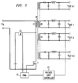
- FIG. 3 works in the same manner as that of FIG. 1 and therefore has corresponding reference numerals. Rather than having only two secondary windings, however, the FIG. 3 embodiment has a group of secondary windings that are wound in the same direction as secondary 21 and another group of secondary winding, wound in the same direction as secondary winding 20. Each secondary winding is coupled to an output filter through a half-wave rectifier circuit in the same manner as described before with reference to secondaries 20 and 21. There is no need that the number of windings be balanced or be equal in any way. For example, there may be a number of secondary windings wound in the same direction as secondary 21 and only a single winding wound as secondary 20. The only requirement is that there be at least two secondary windings, driving two outputs, which are wound in opposite directions.
- the voltage of each of the other outputs V outN is defined by: where n s 1 is the number of turns of secondary winding 20 (corresponding to output V out 1 ), and n sN is the number of turns of the secondary winding corresponding to output V outN . If the feedback were taken from another output, then the voltage of that output rather than V out 1 , would constitute the voltage reference from which other voltages are computed.
- V outN is not dependent on the direction of winding of the corresponding secondary winding. It can be appreciated, then, that the invention offers the opportunity to reduce significantly the cost of equipment for supplying a number of different controlled voltages.
- clamped mode converters are applicable to the circuits of the invention.
- a current loop controller can be added to the feedback circuit, as is known in the art.
- Full-wave rectifiers utilizing tapped or non-tapped windings could be used in place of the half-wave rectifiers, as is also known.
- Various other embodiments and modifications may be made by those skilled in the art without departing from the spirit and scope of the invention.
Landscapes
- Engineering & Computer Science (AREA)
- Power Engineering (AREA)
- Dc-Dc Converters (AREA)
Applications Claiming Priority (2)
| Application Number | Priority Date | Filing Date | Title |
|---|---|---|---|
| US99106792A | 1992-12-15 | 1992-12-15 | |
| US991067 | 1992-12-15 |
Publications (2)
| Publication Number | Publication Date |
|---|---|
| EP0602835A1 true EP0602835A1 (de) | 1994-06-22 |
| EP0602835B1 EP0602835B1 (de) | 1996-05-01 |
Family
ID=25536834
Family Applications (1)
| Application Number | Title | Priority Date | Filing Date |
|---|---|---|---|
| EP93309631A Expired - Lifetime EP0602835B1 (de) | 1992-12-15 | 1993-12-02 | Spannungssteuerschaltungen |
Country Status (4)
| Country | Link |
|---|---|
| US (1) | US5541828A (de) |
| EP (1) | EP0602835B1 (de) |
| JP (1) | JPH06217547A (de) |
| DE (1) | DE69302461T2 (de) |
Cited By (3)
| Publication number | Priority date | Publication date | Assignee | Title |
|---|---|---|---|---|
| US8094466B2 (en) * | 2001-05-09 | 2012-01-10 | Koninklijke Philips Electronics N.V. | Resonant converter |
| CN107368137A (zh) * | 2016-12-19 | 2017-11-21 | 山东金洲科瑞节能科技有限公司 | 交流供电质量调节装置 |
| EP2198506B1 (de) * | 2007-09-05 | 2017-12-27 | Bertelli & Partners S.R.L. | Multifunktions-schaltnetzteil |
Families Citing this family (56)
| Publication number | Priority date | Publication date | Assignee | Title |
|---|---|---|---|---|
| US5303138A (en) * | 1993-04-29 | 1994-04-12 | At&T Bell Laboratories | Low loss synchronous rectifier for application to clamped-mode power converters |
| ES2105957B1 (es) * | 1994-12-30 | 1998-06-01 | Alcatel Standard Electrica | Convertidor multisalida de energia continua-continua. |
| US5590032A (en) | 1995-05-25 | 1996-12-31 | Lucent Technologies Inc. | Self-synchronized drive circuit for a synchronous rectifier in a clamped-mode power converter |
| US5636107A (en) * | 1995-11-15 | 1997-06-03 | International Power Devices, Inc. | DC-DC converters |
| US5648895A (en) * | 1995-12-19 | 1997-07-15 | Sysgration Ltd. | Flyback and charging circuitry for an uninterruptible power supply system |
| US5715153A (en) * | 1996-12-11 | 1998-02-03 | International Power Devices, Inc. | Dual-output DC-DC power supply |
| US5952855A (en) * | 1997-01-03 | 1999-09-14 | General Electric Company | Circuit with multiple output voltages for multiple analog to digital converters |
| US5864472A (en) * | 1997-03-24 | 1999-01-26 | Ault Incorporated | Apparatus for controlling a multiresonant self-oscillating converter circuit |
| US5838558A (en) * | 1997-05-19 | 1998-11-17 | Trw Inc. | Phase staggered full-bridge converter with soft-PWM switching |
| US6011703A (en) * | 1997-07-30 | 2000-01-04 | Lucent Technologies Inc. | Self-synchronized gate drive for power converter employing self-driven synchronous rectifier and method of operation thereof |
| US5982639A (en) * | 1997-11-04 | 1999-11-09 | Power Integrations, Inc. | Two switch off-line switching converter |
| CA2227747A1 (en) * | 1998-01-23 | 1999-07-23 | Gary Arthur Edwards | Buck regulator with plural outputs |
| US6091616A (en) * | 1998-10-21 | 2000-07-18 | Lucent Technologies Inc. | Drive compensation circuit for synchronous rectifier and method of operating the same |
| IE20000021A1 (en) | 1999-01-12 | 2000-09-20 | Artesyn Tech | A post regulation control circuit for a switch mode power supply with multiple outputs. |
| US6310301B1 (en) | 1999-04-08 | 2001-10-30 | Randy T. Heinrich | Inter-substrate conductive mount for a circuit board, circuit board and power magnetic device employing the same |
| US6058026A (en) * | 1999-07-26 | 2000-05-02 | Lucent Technologies, Inc. | Multiple output converter having a single transformer winding and independent output regulation |
| US6246592B1 (en) | 1999-08-10 | 2001-06-12 | Texas Instruments Incorporated | Unique power supply architecture with cascaded converters for large input-to-output step-down ratio |
| US6130828A (en) * | 1999-08-26 | 2000-10-10 | Lucent Technologies, Inc. | Multiple output converter having self-synchronized pulse width modulation regulation |
| US6101111A (en) * | 1999-09-29 | 2000-08-08 | Lucent Technologies, Inc. | Output power control circuit for a flyback converter |
| US6211579B1 (en) | 1999-09-29 | 2001-04-03 | Lucent Technologies, Inc. | Multiple output converter having a low power dissipation cross regulation compensation circuit |
| US6104623A (en) * | 1999-10-21 | 2000-08-15 | Lucent Technologies, Inc. | Multiple output converter having secondary regulator using self-driven synchronous rectifiers |
| US6243278B1 (en) | 2000-04-04 | 2001-06-05 | Tyco Electronics Logistics A.G. | Drive circuit for synchronous rectifier and method of operating the same |
| US6304461B1 (en) * | 2000-06-15 | 2001-10-16 | Supertex, Inc. | DC power converter having bipolar output and bi-directional reactive current transfer |
| US6218891B1 (en) | 2000-07-28 | 2001-04-17 | Lucent Technologies Inc. | Integrated circuit including a driver for a metal-semiconductor field-effect transistor |
| US6396725B1 (en) | 2000-07-31 | 2002-05-28 | Mark E. Jacobs | System and method for improving control loop response of a power supply |
| US6525514B1 (en) * | 2000-08-08 | 2003-02-25 | Power Integrations, Inc. | Method and apparatus for reducing audio noise in a switching regulator |
| US6400580B1 (en) | 2000-10-10 | 2002-06-04 | Wayne C. Bowman | System and method for reducing a DC magnetic flux bias in a transformer and power converter employing the same |
| US6545883B2 (en) | 2001-05-07 | 2003-04-08 | Artesyn Technologies, Inc. | Integrated boost-asymmetrical half-bridge converter |
| JP4108457B2 (ja) * | 2002-11-27 | 2008-06-25 | シャープ株式会社 | スイッチング電源装置 |
| US6917529B2 (en) * | 2003-12-02 | 2005-07-12 | Power-One Limited | Unregulated DC-DC converter having synchronous rectification with efficient gate drives |
| US7196916B2 (en) * | 2005-02-14 | 2007-03-27 | University Of Central Florida Research Foundation | Alternated duty cycle control method for half-bridge DC-DC converter |
| FR2884074B1 (fr) * | 2005-04-01 | 2007-07-06 | Alcatel Converters Sa | Convertisseur a plusieurs voies, a decoupage en cascade et limite en courant |
| JP4335871B2 (ja) * | 2005-12-27 | 2009-09-30 | 新電元工業株式会社 | スイッチング電源装置及びサージ吸収回路 |
| CN100461600C (zh) * | 2006-02-08 | 2009-02-11 | 海韵电子工业股份有限公司 | 一种具瞬时负载的电源供应器 |
| US7583521B2 (en) * | 2006-02-23 | 2009-09-01 | American Power Conversion Corporation | Over voltage clamp |
| US7471524B1 (en) | 2006-05-26 | 2008-12-30 | University Of Central Florida Research Foundation, Inc. | Isolated DC-DC converters with high current capability |
| US7924579B2 (en) * | 2008-02-05 | 2011-04-12 | Cisco Technology, Inc. | Fly-forward converter power supply |
| US8116105B2 (en) | 2008-02-07 | 2012-02-14 | American Power Conversion Corporation | Systems and methods for uninterruptible power supply control |
| US8503201B2 (en) | 2009-12-03 | 2013-08-06 | Schneider Electric It Corporation | Transient clamping circuitry for voltage converter |
| US8199540B2 (en) * | 2010-01-06 | 2012-06-12 | National Taiwan University Of Science And Technology | High voltage gain power converter |
| US8736102B1 (en) | 2010-10-07 | 2014-05-27 | The Boeing Company | Multifunctional power converter |
| US9024474B2 (en) | 2011-08-03 | 2015-05-05 | Schneider Electric It Corporation | UPS mechanical transfer relay arc mitigation |
| US20130077356A1 (en) * | 2011-09-28 | 2013-03-28 | Texas Instruments Incorporated | Dc-dc converters |
| US9281748B2 (en) | 2012-03-02 | 2016-03-08 | Lenovo Enterprise Solutions (Singapore) Pte. Ltd. | Operating a DC-DC converter |
| WO2014032302A1 (en) | 2012-09-03 | 2014-03-06 | Schneider Electric It Corporation | Method and apparatus for controlling distribution of power |
| US9236347B2 (en) | 2013-10-09 | 2016-01-12 | Lenovo Enterprise Solutions (Singapore) Pte. Ltd. | Operating and manufacturing a DC-DC converter |
| US9219422B1 (en) | 2014-08-21 | 2015-12-22 | Lenovo Enterprise Solutions (Singapore) Pte. Ltd. | Operating a DC-DC converter including a coupled inductor formed of a magnetic core and a conductive sheet |
| US9379619B2 (en) | 2014-10-21 | 2016-06-28 | Lenovo Enterprise Solutions (Singapore) Pte. Ltd. | Dividing a single phase pulse-width modulation signal into a plurality of phases |
| CN104777345B (zh) * | 2015-04-22 | 2017-06-13 | 四川英杰电气股份有限公司 | 用于叠层控制电源的电流检测电路、反馈控制电路及电源 |
| US9618539B2 (en) | 2015-05-28 | 2017-04-11 | Lenovo Enterprise Solutions (Singapore) Pte. Ltd. | Sensing current of a DC-DC converter |
| CN105656314A (zh) * | 2016-03-18 | 2016-06-08 | 深圳市陆巡天下科技有限公司 | 一种新型开关电源辅路拓扑 |
| US10833657B2 (en) * | 2018-08-06 | 2020-11-10 | Cirrus Logic, Inc. | Variable output resistance in a playback path with closed-loop pulse-width modulation driver |
| KR20210015333A (ko) | 2019-08-01 | 2021-02-10 | 삼성전자주식회사 | 복수의 전압 레귤레이터들을 포함하는 전자 시스템 |
| CN110572045B (zh) * | 2019-10-15 | 2020-10-09 | 福州大学 | 一种基于双耦合电感的高增益dc-dc变换器 |
| DE102021207153A1 (de) | 2021-07-07 | 2023-01-12 | DIL Deutsches Institut für Lebensmitteltechnik e.V. | Vorrichtung und Verfahren zur kontinuierlichen Ohm´schen Erwärmung von Lebensmitteln |
| US20230207188A1 (en) * | 2021-12-27 | 2023-06-29 | Indian Institute Of Technology Kanpur | Differential transformer based voltage converter and method thereof |
Citations (1)
| Publication number | Priority date | Publication date | Assignee | Title |
|---|---|---|---|---|
| EP0474471A2 (de) * | 1990-09-07 | 1992-03-11 | ITT Industries, Inc. | Festfrequenter Einrichtungsdurchlassumformer mit Nullspannungsschaltung |
Family Cites Families (5)
| Publication number | Priority date | Publication date | Assignee | Title |
|---|---|---|---|---|
| GB8308100D0 (en) * | 1983-03-24 | 1983-05-05 | Rca Corp | Regulated power supply |
| EP0188646B1 (de) * | 1985-01-24 | 1989-12-27 | BULL HN INFORMATION SYSTEMS ITALIA S.p.A. | Einfach geregelte Stromversorgung mit Lastkompensation von einem Hilfsspannungsausgang |
| JPH02241358A (ja) * | 1989-03-10 | 1990-09-26 | Nec Corp | スイッチングレギュレータ |
| IT1231052B (it) * | 1989-09-27 | 1991-11-12 | Bull Hn Information Syst | Alimentatore a commutazione con piu' uscite, regolazione di una tensione di uscita e compensazione di carico. |
| US5400239A (en) * | 1992-12-11 | 1995-03-21 | Northern Telecom Limited | Power converter with plural regulated outputs |
-
1993
- 1993-12-02 DE DE69302461T patent/DE69302461T2/de not_active Expired - Fee Related
- 1993-12-02 EP EP93309631A patent/EP0602835B1/de not_active Expired - Lifetime
- 1993-12-13 JP JP5341163A patent/JPH06217547A/ja active Pending
-
1994
- 1994-11-23 US US08/344,754 patent/US5541828A/en not_active Expired - Lifetime
Patent Citations (1)
| Publication number | Priority date | Publication date | Assignee | Title |
|---|---|---|---|---|
| EP0474471A2 (de) * | 1990-09-07 | 1992-03-11 | ITT Industries, Inc. | Festfrequenter Einrichtungsdurchlassumformer mit Nullspannungsschaltung |
Cited By (3)
| Publication number | Priority date | Publication date | Assignee | Title |
|---|---|---|---|---|
| US8094466B2 (en) * | 2001-05-09 | 2012-01-10 | Koninklijke Philips Electronics N.V. | Resonant converter |
| EP2198506B1 (de) * | 2007-09-05 | 2017-12-27 | Bertelli & Partners S.R.L. | Multifunktions-schaltnetzteil |
| CN107368137A (zh) * | 2016-12-19 | 2017-11-21 | 山东金洲科瑞节能科技有限公司 | 交流供电质量调节装置 |
Also Published As
| Publication number | Publication date |
|---|---|
| JPH06217547A (ja) | 1994-08-05 |
| EP0602835B1 (de) | 1996-05-01 |
| DE69302461D1 (de) | 1996-06-05 |
| DE69302461T2 (de) | 1996-09-05 |
| US5541828A (en) | 1996-07-30 |
Similar Documents
| Publication | Publication Date | Title |
|---|---|---|
| EP0602835B1 (de) | Spannungssteuerschaltungen | |
| US6501193B1 (en) | Power converter having regulated dual outputs | |
| US5838558A (en) | Phase staggered full-bridge converter with soft-PWM switching | |
| US5654881A (en) | Extended range DC-DC power converter circuit | |
| US6831847B2 (en) | Synchronous rectifier drive circuit and power supply including same | |
| US6549436B1 (en) | Integrated magnetic converter circuit and method with improved filtering | |
| EP0759654B1 (de) | Schaltleistungswandler mit kontinuierlichen Eingangs- und Ausgangsstrom | |
| US5418703A (en) | DC-DC converter with reset control for enhanced zero-volt switching | |
| US6775159B2 (en) | Switching power converter circuits providing main and auxiliary output voltages | |
| US5255174A (en) | Regulated bi-directional DC-to-DC voltage converter which maintains a continuous input current during step-up conversion | |
| US5886882A (en) | Push-pull DC-DC converter with transformer having multiple primary and secondary windings with diodes connected between them with MOSFET switching | |
| EP0428377B1 (de) | Gleichspannungs-Schaltwandler-Schaltkreis | |
| US5521807A (en) | DC-To-DC converter with secondary flyback core reset | |
| US6570268B1 (en) | Synchronous rectifier drive circuit and power supply including same | |
| US8169796B2 (en) | Isolated switching power supply apparatus | |
| US6757184B2 (en) | Step-down buck converter with full bridge circuit | |
| US6728118B1 (en) | Highly efficient, tightly regulated DC-to-DC converter | |
| EP0602834B1 (de) | Spannungsteuerschaltungen | |
| JPH0760998B2 (ja) | 全ブリッジ・電力変換回路 | |
| US5293111A (en) | Method for minimizing the switching loss in a power switch | |
| US5140509A (en) | Regulated bi-directional DC-to-DC voltage converter | |
| WO2001052394A2 (en) | Self-driven synchronous rectification circuit for low output voltage dc-dc converters | |
| WO2000028648A1 (en) | A high input voltage, high efficiency, fast transient voltage regulator module (vrm) | |
| US20040246748A1 (en) | Bridge-buck converter with self-driven synchronous rectifiers | |
| EP0966091A2 (de) | Gleichstrom-Gleichstromwandler mit integriertem magnetischem Leistungstransformator |
Legal Events
| Date | Code | Title | Description |
|---|---|---|---|
| PUAI | Public reference made under article 153(3) epc to a published international application that has entered the european phase |
Free format text: ORIGINAL CODE: 0009012 |
|
| AK | Designated contracting states |
Kind code of ref document: A1 Designated state(s): DE FR GB IT |
|
| 17P | Request for examination filed |
Effective date: 19941208 |
|
| 17Q | First examination report despatched |
Effective date: 19950209 |
|
| GRAH | Despatch of communication of intention to grant a patent |
Free format text: ORIGINAL CODE: EPIDOS IGRA |
|
| GRAA | (expected) grant |
Free format text: ORIGINAL CODE: 0009210 |
|
| AK | Designated contracting states |
Kind code of ref document: B1 Designated state(s): DE FR GB IT |
|
| ITF | It: translation for a ep patent filed |
Owner name: JACOBACCI & PERANI S.P.A. |
|
| ET | Fr: translation filed | ||
| REF | Corresponds to: |
Ref document number: 69302461 Country of ref document: DE Date of ref document: 19960605 |
|
| PLBE | No opposition filed within time limit |
Free format text: ORIGINAL CODE: 0009261 |
|
| STAA | Information on the status of an ep patent application or granted ep patent |
Free format text: STATUS: NO OPPOSITION FILED WITHIN TIME LIMIT |
|
| 26N | No opposition filed | ||
| PGFP | Annual fee paid to national office [announced via postgrant information from national office to epo] |
Ref country code: DE Payment date: 19971021 Year of fee payment: 5 |
|
| PGFP | Annual fee paid to national office [announced via postgrant information from national office to epo] |
Ref country code: FR Payment date: 19971023 Year of fee payment: 5 |
|
| PGFP | Annual fee paid to national office [announced via postgrant information from national office to epo] |
Ref country code: GB Payment date: 19971111 Year of fee payment: 5 |
|
| PG25 | Lapsed in a contracting state [announced via postgrant information from national office to epo] |
Ref country code: GB Free format text: LAPSE BECAUSE OF NON-PAYMENT OF DUE FEES Effective date: 19981202 |
|
| GBPC | Gb: european patent ceased through non-payment of renewal fee |
Effective date: 19981202 |
|
| PG25 | Lapsed in a contracting state [announced via postgrant information from national office to epo] |
Ref country code: FR Free format text: LAPSE BECAUSE OF NON-PAYMENT OF DUE FEES Effective date: 19990831 |
|
| REG | Reference to a national code |
Ref country code: FR Ref legal event code: ST |
|
| PG25 | Lapsed in a contracting state [announced via postgrant information from national office to epo] |
Ref country code: DE Free format text: LAPSE BECAUSE OF NON-PAYMENT OF DUE FEES Effective date: 19991201 |
|
| PG25 | Lapsed in a contracting state [announced via postgrant information from national office to epo] |
Ref country code: IT Free format text: LAPSE BECAUSE OF NON-PAYMENT OF DUE FEES;WARNING: LAPSES OF ITALIAN PATENTS WITH EFFECTIVE DATE BEFORE 2007 MAY HAVE OCCURRED AT ANY TIME BEFORE 2007. THE CORRECT EFFECTIVE DATE MAY BE DIFFERENT FROM THE ONE RECORDED. Effective date: 20051202 |