EP0402984B1 - Passive ferroelektrische Flüssigkristall-Anzeigevorrichtung und Verfahren zur Herstellung derselben - Google Patents
Passive ferroelektrische Flüssigkristall-Anzeigevorrichtung und Verfahren zur Herstellung derselben Download PDFInfo
- Publication number
- EP0402984B1 EP0402984B1 EP90201437A EP90201437A EP0402984B1 EP 0402984 B1 EP0402984 B1 EP 0402984B1 EP 90201437 A EP90201437 A EP 90201437A EP 90201437 A EP90201437 A EP 90201437A EP 0402984 B1 EP0402984 B1 EP 0402984B1
- Authority
- EP
- European Patent Office
- Prior art keywords
- liquid crystal
- transmission
- supporting plates
- ferro
- smectic layers
- Prior art date
- Legal status (The legal status is an assumption and is not a legal conclusion. Google has not performed a legal analysis and makes no representation as to the accuracy of the status listed.)
- Expired - Lifetime
Links
- 239000005262 ferroelectric liquid crystals (FLCs) Substances 0.000 title claims description 9
- 238000004519 manufacturing process Methods 0.000 title description 3
- 230000005540 biological transmission Effects 0.000 claims description 30
- 238000011282 treatment Methods 0.000 claims description 23
- 239000004990 Smectic liquid crystal Substances 0.000 claims description 21
- 239000004973 liquid crystal related substance Substances 0.000 claims description 18
- 238000000034 method Methods 0.000 claims description 11
- 230000005684 electric field Effects 0.000 claims description 6
- 125000006850 spacer group Chemical group 0.000 claims description 6
- 238000007669 thermal treatment Methods 0.000 claims description 3
- 230000003746 surface roughness Effects 0.000 claims description 2
- 239000000758 substrate Substances 0.000 claims 2
- 230000007547 defect Effects 0.000 description 12
- 239000000463 material Substances 0.000 description 6
- 230000007704 transition Effects 0.000 description 6
- 238000001816 cooling Methods 0.000 description 5
- 230000001419 dependent effect Effects 0.000 description 4
- 238000009826 distribution Methods 0.000 description 4
- 230000007423 decrease Effects 0.000 description 2
- 239000002305 electric material Substances 0.000 description 2
- 230000015654 memory Effects 0.000 description 2
- 230000003287 optical effect Effects 0.000 description 2
- 239000002245 particle Substances 0.000 description 2
- 230000010287 polarization Effects 0.000 description 2
- 230000008569 process Effects 0.000 description 2
- VYPSYNLAJGMNEJ-UHFFFAOYSA-N silicon dioxide Inorganic materials O=[Si]=O VYPSYNLAJGMNEJ-UHFFFAOYSA-N 0.000 description 2
- 238000009827 uniform distribution Methods 0.000 description 2
- 239000004952 Polyamide Substances 0.000 description 1
- 239000004642 Polyimide Substances 0.000 description 1
- 239000004372 Polyvinyl alcohol Substances 0.000 description 1
- 230000009471 action Effects 0.000 description 1
- 230000006399 behavior Effects 0.000 description 1
- 238000006243 chemical reaction Methods 0.000 description 1
- 239000004020 conductor Substances 0.000 description 1
- 230000008878 coupling Effects 0.000 description 1
- 238000010168 coupling process Methods 0.000 description 1
- 238000005859 coupling reaction Methods 0.000 description 1
- 230000008021 deposition Effects 0.000 description 1
- 230000001627 detrimental effect Effects 0.000 description 1
- 230000000694 effects Effects 0.000 description 1
- 230000001747 exhibiting effect Effects 0.000 description 1
- 239000011521 glass Substances 0.000 description 1
- 238000010438 heat treatment Methods 0.000 description 1
- AMGQUBHHOARCQH-UHFFFAOYSA-N indium;oxotin Chemical compound [In].[Sn]=O AMGQUBHHOARCQH-UHFFFAOYSA-N 0.000 description 1
- 230000003993 interaction Effects 0.000 description 1
- 239000007788 liquid Substances 0.000 description 1
- 230000005577 local transmission Effects 0.000 description 1
- 238000005259 measurement Methods 0.000 description 1
- 230000004048 modification Effects 0.000 description 1
- 238000012986 modification Methods 0.000 description 1
- 229920002647 polyamide Polymers 0.000 description 1
- 229920001721 polyimide Polymers 0.000 description 1
- 229920000642 polymer Polymers 0.000 description 1
- 229920002451 polyvinyl alcohol Polymers 0.000 description 1
- 239000010453 quartz Substances 0.000 description 1
- 230000009467 reduction Effects 0.000 description 1
- 229910052814 silicon oxide Inorganic materials 0.000 description 1
- 230000002269 spontaneous effect Effects 0.000 description 1
- 230000006641 stabilisation Effects 0.000 description 1
- 239000000126 substance Substances 0.000 description 1
Images

Classifications
-
- G—PHYSICS
- G02—OPTICS
- G02F—OPTICAL DEVICES OR ARRANGEMENTS FOR THE CONTROL OF LIGHT BY MODIFICATION OF THE OPTICAL PROPERTIES OF THE MEDIA OF THE ELEMENTS INVOLVED THEREIN; NON-LINEAR OPTICS; FREQUENCY-CHANGING OF LIGHT; OPTICAL LOGIC ELEMENTS; OPTICAL ANALOGUE/DIGITAL CONVERTERS
- G02F1/00—Devices or arrangements for the control of the intensity, colour, phase, polarisation or direction of light arriving from an independent light source, e.g. switching, gating or modulating; Non-linear optics
- G02F1/01—Devices or arrangements for the control of the intensity, colour, phase, polarisation or direction of light arriving from an independent light source, e.g. switching, gating or modulating; Non-linear optics for the control of the intensity, phase, polarisation or colour
- G02F1/13—Devices or arrangements for the control of the intensity, colour, phase, polarisation or direction of light arriving from an independent light source, e.g. switching, gating or modulating; Non-linear optics for the control of the intensity, phase, polarisation or colour based on liquid crystals, e.g. single liquid crystal display cells
- G02F1/137—Devices or arrangements for the control of the intensity, colour, phase, polarisation or direction of light arriving from an independent light source, e.g. switching, gating or modulating; Non-linear optics for the control of the intensity, phase, polarisation or colour based on liquid crystals, e.g. single liquid crystal display cells characterised by the electro-optical or magneto-optical effect, e.g. field-induced phase transition, orientation effect, guest-host interaction or dynamic scattering
- G02F1/139—Devices or arrangements for the control of the intensity, colour, phase, polarisation or direction of light arriving from an independent light source, e.g. switching, gating or modulating; Non-linear optics for the control of the intensity, phase, polarisation or colour based on liquid crystals, e.g. single liquid crystal display cells characterised by the electro-optical or magneto-optical effect, e.g. field-induced phase transition, orientation effect, guest-host interaction or dynamic scattering based on orientation effects in which the liquid crystal remains transparent
- G02F1/141—Devices or arrangements for the control of the intensity, colour, phase, polarisation or direction of light arriving from an independent light source, e.g. switching, gating or modulating; Non-linear optics for the control of the intensity, phase, polarisation or colour based on liquid crystals, e.g. single liquid crystal display cells characterised by the electro-optical or magneto-optical effect, e.g. field-induced phase transition, orientation effect, guest-host interaction or dynamic scattering based on orientation effects in which the liquid crystal remains transparent using ferroelectric liquid crystals
-
- G—PHYSICS
- G02—OPTICS
- G02F—OPTICAL DEVICES OR ARRANGEMENTS FOR THE CONTROL OF LIGHT BY MODIFICATION OF THE OPTICAL PROPERTIES OF THE MEDIA OF THE ELEMENTS INVOLVED THEREIN; NON-LINEAR OPTICS; FREQUENCY-CHANGING OF LIGHT; OPTICAL LOGIC ELEMENTS; OPTICAL ANALOGUE/DIGITAL CONVERTERS
- G02F1/00—Devices or arrangements for the control of the intensity, colour, phase, polarisation or direction of light arriving from an independent light source, e.g. switching, gating or modulating; Non-linear optics
- G02F1/01—Devices or arrangements for the control of the intensity, colour, phase, polarisation or direction of light arriving from an independent light source, e.g. switching, gating or modulating; Non-linear optics for the control of the intensity, phase, polarisation or colour
- G02F1/13—Devices or arrangements for the control of the intensity, colour, phase, polarisation or direction of light arriving from an independent light source, e.g. switching, gating or modulating; Non-linear optics for the control of the intensity, phase, polarisation or colour based on liquid crystals, e.g. single liquid crystal display cells
- G02F1/133—Constructional arrangements; Operation of liquid crystal cells; Circuit arrangements
- G02F1/1333—Constructional arrangements; Manufacturing methods
- G02F1/1337—Surface-induced orientation of the liquid crystal molecules, e.g. by alignment layers
- G02F1/133753—Surface-induced orientation of the liquid crystal molecules, e.g. by alignment layers with different alignment orientations or pretilt angles on a same surface, e.g. for grey scale or improved viewing angle
-
- G—PHYSICS
- G02—OPTICS
- G02F—OPTICAL DEVICES OR ARRANGEMENTS FOR THE CONTROL OF LIGHT BY MODIFICATION OF THE OPTICAL PROPERTIES OF THE MEDIA OF THE ELEMENTS INVOLVED THEREIN; NON-LINEAR OPTICS; FREQUENCY-CHANGING OF LIGHT; OPTICAL LOGIC ELEMENTS; OPTICAL ANALOGUE/DIGITAL CONVERTERS
- G02F1/00—Devices or arrangements for the control of the intensity, colour, phase, polarisation or direction of light arriving from an independent light source, e.g. switching, gating or modulating; Non-linear optics
- G02F1/01—Devices or arrangements for the control of the intensity, colour, phase, polarisation or direction of light arriving from an independent light source, e.g. switching, gating or modulating; Non-linear optics for the control of the intensity, phase, polarisation or colour
- G02F1/13—Devices or arrangements for the control of the intensity, colour, phase, polarisation or direction of light arriving from an independent light source, e.g. switching, gating or modulating; Non-linear optics for the control of the intensity, phase, polarisation or colour based on liquid crystals, e.g. single liquid crystal display cells
- G02F1/133—Constructional arrangements; Operation of liquid crystal cells; Circuit arrangements
- G02F1/1333—Constructional arrangements; Manufacturing methods
- G02F1/133371—Cells with varying thickness of the liquid crystal layer
-
- G—PHYSICS
- G02—OPTICS
- G02F—OPTICAL DEVICES OR ARRANGEMENTS FOR THE CONTROL OF LIGHT BY MODIFICATION OF THE OPTICAL PROPERTIES OF THE MEDIA OF THE ELEMENTS INVOLVED THEREIN; NON-LINEAR OPTICS; FREQUENCY-CHANGING OF LIGHT; OPTICAL LOGIC ELEMENTS; OPTICAL ANALOGUE/DIGITAL CONVERTERS
- G02F1/00—Devices or arrangements for the control of the intensity, colour, phase, polarisation or direction of light arriving from an independent light source, e.g. switching, gating or modulating; Non-linear optics
- G02F1/01—Devices or arrangements for the control of the intensity, colour, phase, polarisation or direction of light arriving from an independent light source, e.g. switching, gating or modulating; Non-linear optics for the control of the intensity, phase, polarisation or colour
- G02F1/13—Devices or arrangements for the control of the intensity, colour, phase, polarisation or direction of light arriving from an independent light source, e.g. switching, gating or modulating; Non-linear optics for the control of the intensity, phase, polarisation or colour based on liquid crystals, e.g. single liquid crystal display cells
- G02F1/133—Constructional arrangements; Operation of liquid crystal cells; Circuit arrangements
- G02F1/1333—Constructional arrangements; Manufacturing methods
- G02F1/1337—Surface-induced orientation of the liquid crystal molecules, e.g. by alignment layers
- G02F1/133753—Surface-induced orientation of the liquid crystal molecules, e.g. by alignment layers with different alignment orientations or pretilt angles on a same surface, e.g. for grey scale or improved viewing angle
- G02F1/133761—Surface-induced orientation of the liquid crystal molecules, e.g. by alignment layers with different alignment orientations or pretilt angles on a same surface, e.g. for grey scale or improved viewing angle with different pretilt angles
-
- G—PHYSICS
- G02—OPTICS
- G02F—OPTICAL DEVICES OR ARRANGEMENTS FOR THE CONTROL OF LIGHT BY MODIFICATION OF THE OPTICAL PROPERTIES OF THE MEDIA OF THE ELEMENTS INVOLVED THEREIN; NON-LINEAR OPTICS; FREQUENCY-CHANGING OF LIGHT; OPTICAL LOGIC ELEMENTS; OPTICAL ANALOGUE/DIGITAL CONVERTERS
- G02F1/00—Devices or arrangements for the control of the intensity, colour, phase, polarisation or direction of light arriving from an independent light source, e.g. switching, gating or modulating; Non-linear optics
- G02F1/01—Devices or arrangements for the control of the intensity, colour, phase, polarisation or direction of light arriving from an independent light source, e.g. switching, gating or modulating; Non-linear optics for the control of the intensity, phase, polarisation or colour
- G02F1/13—Devices or arrangements for the control of the intensity, colour, phase, polarisation or direction of light arriving from an independent light source, e.g. switching, gating or modulating; Non-linear optics for the control of the intensity, phase, polarisation or colour based on liquid crystals, e.g. single liquid crystal display cells
- G02F1/133—Constructional arrangements; Operation of liquid crystal cells; Circuit arrangements
- G02F1/1333—Constructional arrangements; Manufacturing methods
- G02F1/1339—Gaskets; Spacers; Sealing of cells
- G02F1/13392—Gaskets; Spacers; Sealing of cells spacers dispersed on the cell substrate, e.g. spherical particles, microfibres
-
- G—PHYSICS
- G02—OPTICS
- G02F—OPTICAL DEVICES OR ARRANGEMENTS FOR THE CONTROL OF LIGHT BY MODIFICATION OF THE OPTICAL PROPERTIES OF THE MEDIA OF THE ELEMENTS INVOLVED THEREIN; NON-LINEAR OPTICS; FREQUENCY-CHANGING OF LIGHT; OPTICAL LOGIC ELEMENTS; OPTICAL ANALOGUE/DIGITAL CONVERTERS
- G02F2203/00—Function characteristic
- G02F2203/30—Gray scale
Definitions
- the invention relates to a liquid crystal device according to the preamble of claim 1.
- Such a device is suitable, for example as a light shutter.
- the invention also relates to a display device according to the preamble at claim 2.
- EP-A-240 010 which employs smectic layers perpendicular to the surfaces of the supporting plates and alignment control layers having regions of different alignment control power.
- Such a device is suitable for passively driven matrices having large numbers of lines. Since the contrast is maintained, the device is very suitable for LCD TV, but also for datagraphic applications.
- One of the objects of the invention is to eliminate these drawbacks by providing a display device in which grey scales can be realised with easily realisable signals on row as well as column electrodes, while the data voltages on the column electrodes can be kept so low that possible crosstalk does not affect or hardly affects the electro-optical transmission value (grey scale) of the display medium. It is another object of the invention to provide a display device in which the use of picture memories is not necessary, while there is less loss of brightness.
- the invention is based, inter alia , on the recognition that the threshold voltage in the transmission/voltage characteristic is also determined by the angle of the smectic layers of the ferro-electric molecules with respect to the supporting plates.
- a liquid crystal device according to the invention is characterized by the characterising features of claim 1.
- a liquid crystal display device is characterised by the characterising features of claim 2.
- threshold voltages of local transmission/voltage characteristics are uniformly distributed across the pixel, as viewed on a microscale, which distribution, as viewed on a macroscale, becomes manifest in a transmission/voltage characteristic having a faint slope whose transition range has a width of at least 0.5 Volt.
- the width of the transition range is understood to mean the voltage range within which the transmission increases or decreases from 10% to 90% of its maximum value.
- a preferred embodiment of a device according to the invention therefore comprises at least 10 spacers per pixel.
- needle defects At the area of these needle defects (which are not only introduced by spacer particles but also, for example by a fast cooling of the liquid crystal material or by a rubbing treatment of the orienting surface) the areas with different angles of the smectic layers, or threshold voltages are produced by a treatment in an electric field with a high field strength.
- the length of the needle defects which may detrimentally influence the transmission/voltage characteristic, can be reduced by a treatment in an electric field with a low field strength.
- Low-frequency is herein understood to mean a frequency of 0.1-200 Hz.
- the duration of the treatment is of the order of 0.5-2 minutes and, likewise as the field strength, it is also dependent on the liquid crystal material used.
- the relevant spread can also be obtained by subjecting the pixels after filling to a local thermal treatment (for example, laser irradiation) while traversing the smectic A-smectic C trajectory.
- a local thermal treatment for example, laser irradiation
- the spread may also be obtained mechanically, chemically, magnetically or in another process; in this respect it may be advantageous to give the device a pretreatment introducing inhomogeneities.
- the device In order to reduce the influence of previous picture contents as much as possible in the device thus obtained, it is preferably adapted in such a way that a desired transmission state is reached from an extreme transmission state during line selection.
- Fig. 1 shows diagrammatically a part of a surface-stabilized ferro-electric display device 1 according to the invention.
- Row and column electrodes or other electrodes (not shown) of conducting materials such as, for example, indium-tin-oxide (ITO) are provided on the two supporting plates 2 and 3 of, for example glass or quartz.
- the device also comprises polarizers which are not shown.
- the orientation layers 4 of, for example polyimide, polyamide or polyvinyl alcohol are subjected to a suitable rubbing treatment whereafter the liquid crystal material (in this example ZLI 3654 of the firm of Merck) is introduced in the isotropic phase into the display device, whereafter it is slowly cooled down via the nematic phase and the smectic A phase to the smectic C phase.
- the layers 6 in a device according to the invention do not have the completely perpendicular structure, but as a result of interactions of the liquid crystal molecules with the orienting layers 4 they have a kinked or "chevron" structure.
- These layers 6′, 6 ⁇ and 6 extend at an angle ⁇ at the location of the supporting plates 2, 3 with respect to the normal on the supporting plates 2 and 3.
- the possible positions of the molecules (director) on the cone are limited in both situations in the fieldless state to the positions (a) and (b) in the layer 6, and (a′) and (b′) in the layer 6′. Optically, this means that the two states have different switching angles 2 ⁇ 1 and 2 ⁇ 2.
- the directors flip over, for example from position a(a′) to position b(b′).
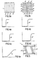
- Fig. 3 shows (partly or not) a pixel 7 which is subdivided into sub-areas 8a ..., 8b ...., 8c ..., 8d .... at which the value of the angle ⁇ decreases from 8a to 8d.
- the sub-areas may be mutually arranged in different manners, as is shown in Figs. 3a and 3b. A more arbitrary distribution is also possible.
- Fig. 4 shows the transmission/voltage characteristics 9a, 9b, 9c, 9d associated with the sub-areas 8a, 8b, 8c, 8d, measured at a fixed pulse duration, and the transmission/voltage characteristic associated with the overall area.
- the distribution of sub-areas having steep transmission/voltage characteristics and different threshold voltages across a pixel leads to a transmission/voltage characteristic having a wide transition range Ca less steep slope) for the entire pixel, which provides the possibility of adjusting grey scales.
- the curve 10 can be explained from the fact that for a uniform distribution of the sub-areas 8 the areas with a low threshold voltage switch first at an increasing voltage, subsequently those with a slightly higher voltage, etc.
- the width of the transmission/voltage characteristic 10 may thereby be adjusted at a value of approximately 0.5-10 Volts.
- a pixel is brought to an extreme state before it is driven, as is described in greater detail in NL-A 870340 (PHN 12.352).
- Other drive schemes such as the so-called “AC stabilisation” method, are alternatively possible.
- the variation in the angle ⁇ (or in the apex angle of the "chevron") can be obtained in different manners.
- needle defects are usually produced. These needle defects are produced generally at the location of inhomogeneities such as, for example, spacer spheres and are comparable with so-called "zigzag defects" at which the angle ⁇ within the defect is opposed to that outside it.
- An electric voltage treatment at a low frequency in the relevant example a square-wave voltage of ⁇ 2 V, 20 Hz for 2 minutes causes these needle defects to shrink to minimum dimensions ( ⁇ 10 ⁇ m).
- a subsequent treatment at a higher voltage ⁇ 10 V, 20 Hz, 1 minute
- areas with different ⁇ will grow, generally starting at one of the remainders of the needle defects.
- a uniform distribution of such areas can thus be obtained by increasing the number of needle defects, for example, by a large number of spacer particles ( ⁇ 10 per pixel which may be uniformly distributed, for example, by means of photolithographic methods or other methods), accelerated cooling or a special rubbing treatment (notably a low-energy rubbing treatment).
- a larger threshold voltage spread of the areas and hence a faint transmission/voltage characteristic of the device can be obtained by subjecting the devices subsequently to treatments with different electric voltages, for example, first ⁇ 12.5 V, ⁇ 15 V, ⁇ 17.5 V, ⁇ 20 V, all at 20 Hz and for 1 minute.
- the threshold voltage and the slope of the transmission/voltage characteristic can be adjusted, dependent on the ferro-electric material and the thickness of the liquid crystal (approximately 1.6 ⁇ m in this case).
- the threshold voltage spread can also be introduced by firstly giving the device a low-frequency alternating voltage treatment at a fairly high voltage (in the example of ZLI 3654, for example, ⁇ 15 V, 20 Hz, for 1 minute) so that many extra regions with a varying ⁇ are produced on the sides of the needle defects, and by subsequently reducing the still present needle defects for a large part by means of a treatment at a low electric voltage ( ⁇ 2 V, 20 Hz, 2 minutes). Areas with different ⁇ are then distributed across a pixel in such a way that a faint transmission/voltage curve is obtained.
- a fairly high voltage in the example of ZLI 3654, for example, ⁇ 15 V, 20 Hz, for 1 minute
- the treatment may be continued by means of an extra treatment at a higher voltage (approx. 25 V, approx. 30 V) for 1 to 5 minutes.
- a higher voltage approximately 25 V, approx. 30 V
- the distribution over different angles ⁇ now becomes slightly narrower (closer to 0°), so that a less wide transition range in the transmission/voltage curve is obtained, the maximum transmission is higher which results in a better contrast.
- the device is now less sensitive to crosstalk.
- the variation of the angle ⁇ can also be obtained by varying the rubbing pressure during rubbing of the orientation layer 4, or by using a spread in the rubbing energy.
- the orientation layer 4 may also be composed of, for example polymer types which cannot be fully mixed, or certain reactions (for example, curing of the orientation layer) can be influenced chemically or thermally or through irradiation in different manners.
- the orientation layer may also be obtained by (oblique) vapour deposition of silicon oxide or by other known techniques.
- a combination of an electric field treatment and a chemical treatment of the liquid crystal material may be considered whereby this variation can be obtained, notably treatments influencing the viscosity and the elastic constants and/or the spontaneous polarization.
- An electrical, magnetical or mechanical treatment may also be considered, by which the smectic layers are deformed, or a thermal treatment of temporary heating or cooling the sub-areas or of providing a thermal gradient.
- a device according to the invention may alternatively be used in other applications where a faint transmission/voltage curve is desired, for example, in dashboard display devices.
- the layers 6 need not necessarily have a kink but may alternatively be planar (layers 6 ii in Fig. 5), with the angles of the layers 6 iii exhibiting a spread with respect to the supporting plates. Moreover, the kink of the "chevron" need not necessarily be right in the centre of the smectic layer (see 6 iv in Fig. 5).
Landscapes
- Physics & Mathematics (AREA)
- Nonlinear Science (AREA)
- Chemical & Material Sciences (AREA)
- Crystallography & Structural Chemistry (AREA)
- General Physics & Mathematics (AREA)
- Optics & Photonics (AREA)
- Mathematical Physics (AREA)
- Spectroscopy & Molecular Physics (AREA)
- Liquid Crystal (AREA)
Claims (10)
- Flüssigkristallanordnung mit einer allmählichen Transmissions/Spannungskennlinie, mit einem ferroelektrischen Flüssigkristallmittel mit smektischen Schichten zwischen zwei Trägerplatten mit Elektroden zum Bestimmen eines elektrooptischen Elements, das örtlich verschiedene Schweflenkennlinien hat, dadurch gekennzeichnet, daß im Bereich des elektrooptischen Elements die Winkel zwischen den smektischen Schichten und wenigstens einem der Substrate eine Streuung aufweisen.
- Eine Flüssigkristall-Wiedergabeanordnung mit einer allmählichen Transmissions/Spannungskennlinie mit einem ferroelektrischen Flüssigkristallmittel mit smektischen Schichten zwischen zwei Trägerplatten, von denen die erste ein System von Zeilenelektroden und die zweite eine Gruppe von Spaltenelektroden zum Bestimmen von Bildelementen an den Kreuzpunkten der Zeilen- und Spaltenelektroden enthält, wobei jedes Bildelement örtlich verschiedene Schwellenkennlinien hat, dadurch gekennzeichnet, daß im Bereich jedes Bildelements die Winkel zwischen den smektischen Schichten und wenigstens einem der Substrate eine Streuung aufweisen.
- Anordnung nach Anspruch 1 oder 2, dadurch gekennzeichnet, daß wenigstens eine der Elektroden eine Streuung im Grade ihrer Oberflächenrauheit an der Stelle des elektrooptischen Elements oder an der Stelle des Bildelements aufweist.
- Anordnung nach Anspruch 1, 2 oder 3, dadurch gekennzeichnet, daß die Breite des Transmissionsbereichs in der Transmissions/Spannungskennlinie wenigstens 0,5 Volt beträgt.
- Anordnung nach einem der Ansprüche 1 bis 4, dadurch gekennzeichnet, daß Distanzstücke im Bereich der Bildelemente angeordnet sind.
- Anordnung nach einem der Ansprüche 2 bis 5, dadurch gekennzeichnet, daß die Anordnung Mittel zum Anlegen von Spannungsimpulsen mit fester Impulsdauer an die Bildelemente enthält, wobei die Spannung eines Impulses die Transmission bestimmt.
- Wiedergabeanordnung nach Anspruch 6, dadurch gekennzeichnet, daß sie Mittel zum Überführen der Bildelemente in einen extremen Transmissionszustand vor dem Anlegen der Spannungsimpulse enthält.
- Verfahren zum Erhalten einer allmählichen Transmissions/Spannungskennlinie in einer Flüssigkristallanordnung mit einem ferroelektrischen Flüssigkristallmittel mit smektischen Schichten zwischen zwei Trägerplatten mit Elektroden, die ein elektrooptisches Element oder Bildelemente bestimmen, dadurch gekennzeichnet, daß die Anordnung wenigstens eine Niederfrequenz-Elektrofeldbehandlung bei niedriger Feldstärke erfährt, wodurch eine Streuung in den Winkeln der smektischen Schichten in bezug auf wenigstens eine der Trägerplatten erfährt.
- Verfahren zum Erhalten einer allmählichen Transmissions/Spannungskennlinie in einer Flüssigkristallanordnung mit einem ferroelektrischen Flüssigkristallmittel mit smektischen Schichten zwischen zwei Trägerplatten mit Elektroden, die ein elektrooptisches Element oder Bildelemente bestimmen, dadurch gekennzeichnet, daß die Anordnung eine Wärmebehandlung erfährt, die eine Streuung von Winkeln der smektischen Schichten in bezug auf wenigstens eine der Trägerplatten ergibt.
- Verfahren zum Erhalten einer allmählichen Transmissions/Spannungskennlinie in einer Flüssigkristallanordnung mit einem ferroelektrischen Flüssigkristallmedium mit smektischen Schichten zwischen zwei Trägerplatten mit Elektroden, die ein elektrooptisches Element oder Bildelemente bestimmen, dadurch gekennzeichnet, daß die Anordnung eine mechanische Behandlung erfährt, die eine Streuung von Winkeln der smektischen Schichten in bezug auf wenigstens eine der Trägerplatten ergibt.
Applications Claiming Priority (2)
| Application Number | Priority Date | Filing Date | Title |
|---|---|---|---|
| NL8901481A NL8901481A (nl) | 1989-06-12 | 1989-06-12 | Passieve ferro-elektrisch vloeibaar kristal weergeefinrichting en werkwijze ter vervaardiging daarvan. |
| NL8901481 | 1989-06-12 |
Publications (2)
| Publication Number | Publication Date |
|---|---|
| EP0402984A1 EP0402984A1 (de) | 1990-12-19 |
| EP0402984B1 true EP0402984B1 (de) | 1994-12-14 |
Family
ID=19854816
Family Applications (1)
| Application Number | Title | Priority Date | Filing Date |
|---|---|---|---|
| EP90201437A Expired - Lifetime EP0402984B1 (de) | 1989-06-12 | 1990-06-06 | Passive ferroelektrische Flüssigkristall-Anzeigevorrichtung und Verfahren zur Herstellung derselben |
Country Status (7)
| Country | Link |
|---|---|
| US (1) | US5151804A (de) |
| EP (1) | EP0402984B1 (de) |
| JP (1) | JPH0325417A (de) |
| KR (1) | KR910001436A (de) |
| DE (1) | DE69015005T2 (de) |
| HK (1) | HK170196A (de) |
| NL (1) | NL8901481A (de) |
Families Citing this family (25)
| Publication number | Priority date | Publication date | Assignee | Title |
|---|---|---|---|---|
| US5293544A (en) * | 1989-03-07 | 1994-03-08 | Canon Kabushiki Kaisha | Liquid crystal apparatus including panel having plural bent layers of liquid crystal molecules |
| JP2802685B2 (ja) * | 1991-01-08 | 1998-09-24 | キヤノン株式会社 | 強誘電性液晶装置 |
| US5347381B1 (en) * | 1991-01-25 | 1997-07-01 | Sharp Kk | Ferroelectric liquid crystal display device with molecules between hairpin and lightning defects following the lightning defects |
| JPH04258924A (ja) * | 1991-02-13 | 1992-09-14 | Canon Inc | カイラルスメクチック液晶素子およびその製造方法 |
| JP3076085B2 (ja) * | 1991-04-27 | 2000-08-14 | 株式会社半導体エネルギー研究所 | 液晶電気光学装置 |
| JP2713513B2 (ja) * | 1991-08-29 | 1998-02-16 | シャープ株式会社 | 液晶表示装置 |
| US5353141A (en) * | 1991-10-08 | 1994-10-04 | Canon Kabushiki Kaisha | Method for aligning treatment of liquid crystal device including varying with time the feeding speed of the rubbing roller |
| JP2877601B2 (ja) * | 1992-01-10 | 1999-03-31 | 松下電器産業株式会社 | 液晶表示装置とその製造法 |
| DE69320073T2 (de) * | 1992-01-24 | 1999-02-25 | Canon K.K., Tokio/Tokyo | Verfahren zur Behandlung einer chiralen smektischen Flüssigkristallvorrichtung |
| US5455695A (en) * | 1992-01-27 | 1995-10-03 | Canon Kabushiki Kaisha | Process for producing liquid crystal device including rubbing with two rubbing rollers rotating in same directions at different speeds |
| JPH05273554A (ja) * | 1992-01-29 | 1993-10-22 | Canon Inc | 強誘電性液晶素子 |
| TW476422U (en) * | 1992-01-29 | 2002-02-11 | Sharp Kk | Liquid crystal display |
| JP3456493B2 (ja) * | 1992-10-24 | 2003-10-14 | ソニー株式会社 | 液晶素子 |
| US5631752A (en) * | 1992-12-24 | 1997-05-20 | Casio Computer Co., Ltd. | Antiferroelectric liquid crystal display element exhibiting a precursor tilt phenomenon |
| US5781266A (en) * | 1993-09-27 | 1998-07-14 | Matsushita Electric Industrial Co., Ltd. | Ferroelectric liquid crystal display device and method for producing the same |
| US5510914A (en) * | 1993-11-15 | 1996-04-23 | The Regents Of The University Of Colorado | Smectic liquid crystal analog phase modulator |
| US5623354A (en) * | 1994-02-10 | 1997-04-22 | International Business Machines Corporation | Liquid crystal display with multi-domains |
| GB2293260B (en) * | 1994-09-19 | 1998-07-08 | Sharp Kk | Liquid crystal device |
| US5847799A (en) * | 1995-05-31 | 1998-12-08 | Casio Computer Co., Ltd. | Antiferroelectric liquid crystal display device |
| US5724116A (en) * | 1995-06-06 | 1998-03-03 | Citizen Watch Co., Ltd. | Liquid crystal panel with memory function |
| DE69625889D1 (de) * | 1995-07-03 | 2003-02-27 | Citizen Watch Co Ltd | Flüssigkristallvorrichtung |
| US6175401B1 (en) * | 1997-05-02 | 2001-01-16 | Casio Computer Co., Ltd. | Liquid crystal display device having a liquid crystal layer which contains liquid crystal molecules in a plurality of alignment state and method for driving the same |
| JP3551702B2 (ja) * | 1997-05-08 | 2004-08-11 | カシオ計算機株式会社 | 液晶表示素子とその駆動方法 |
| KR101500684B1 (ko) * | 2008-04-17 | 2015-03-10 | 삼성디스플레이 주식회사 | 캐리어 기판 및 이를 이용한 가요성 표시 장치의 제조 방법 |
| US8821970B2 (en) | 2009-05-22 | 2014-09-02 | Corning Incorporated | Slip agent for protecting glass |
Family Cites Families (11)
| Publication number | Priority date | Publication date | Assignee | Title |
|---|---|---|---|---|
| GB1601601A (en) * | 1978-01-18 | 1981-11-04 | Standard Telephones Cables Ltd | Liquid crystal display cells |
| GB2173336B (en) * | 1985-04-03 | 1988-04-27 | Stc Plc | Addressing liquid crystal cells |
| JPH0723942B2 (ja) * | 1985-08-08 | 1995-03-15 | 株式会社半導体エネルギ−研究所 | 液晶装置 |
| SE8504761D0 (sv) * | 1985-10-14 | 1985-10-14 | Sven Torbjorn Lagerwall | Improvements of ferroelectric liquid crystal devices |
| JPS62124525A (ja) * | 1985-11-25 | 1987-06-05 | Semiconductor Energy Lab Co Ltd | 液晶装置 |
| JPS62159124A (ja) * | 1986-01-07 | 1987-07-15 | Semiconductor Energy Lab Co Ltd | 液晶装置 |
| US4796980A (en) * | 1986-04-02 | 1989-01-10 | Canon Kabushiki Kaisha | Ferroelectric liquid crystal optical modulation device with regions within pixels to initiate nucleation and inversion |
| US4932758A (en) * | 1987-09-17 | 1990-06-12 | Canon Kabushiki Kaisha | Ferroelectric smectic liquid crystal device having a bistable alignment state providing two stable orientation states |
| EP0310403B1 (de) * | 1987-09-29 | 1995-06-14 | Semiconductor Energy Laboratory Co., Ltd. | Elektrooptische Flüssigkristallvorrichtung |
| NL8703085A (nl) * | 1987-12-21 | 1989-07-17 | Philips Nv | Werkwijze voor het besturen van een weergeefinrichting. |
| EP0327071B1 (de) * | 1988-02-02 | 1995-05-03 | Seiko Epson Corporation | Elektro-optische Vorrichtung |
-
1989
- 1989-06-12 NL NL8901481A patent/NL8901481A/nl not_active Application Discontinuation
-
1990
- 1990-06-06 EP EP90201437A patent/EP0402984B1/de not_active Expired - Lifetime
- 1990-06-06 DE DE69015005T patent/DE69015005T2/de not_active Expired - Fee Related
- 1990-06-11 US US07/535,809 patent/US5151804A/en not_active Expired - Fee Related
- 1990-06-11 KR KR1019900008503A patent/KR910001436A/ko not_active Ceased
- 1990-06-12 JP JP2151799A patent/JPH0325417A/ja active Pending
-
1996
- 1996-09-12 HK HK170196A patent/HK170196A/en not_active IP Right Cessation
Also Published As
| Publication number | Publication date |
|---|---|
| DE69015005D1 (de) | 1995-01-26 |
| HK170196A (en) | 1996-09-20 |
| DE69015005T2 (de) | 1995-06-22 |
| US5151804A (en) | 1992-09-29 |
| EP0402984A1 (de) | 1990-12-19 |
| NL8901481A (nl) | 1991-01-02 |
| KR910001436A (ko) | 1991-01-30 |
| JPH0325417A (ja) | 1991-02-04 |
Similar Documents
| Publication | Publication Date | Title |
|---|---|---|
| EP0402984B1 (de) | Passive ferroelektrische Flüssigkristall-Anzeigevorrichtung und Verfahren zur Herstellung derselben | |
| EP0240010B1 (de) | Optische Modulationsvorrichtung | |
| KR100208475B1 (ko) | 자기장 처리에 의한 액정배향막의 제조방법 | |
| US5552914A (en) | Liquid crystal display having a fine particle-dispersion layer on at least one side of the liquid crystal layer | |
| EP1042702B1 (de) | Bistabile nematische flüssigkristallvorrichtung | |
| Goodman | Liquid-crystal displays—Electro-optic effects and addressing techniques | |
| KR100220756B1 (ko) | 반강유전성 액정을 포함하는 액정판넬 및 그의 제조방법 | |
| EP0622657B1 (de) | Flüssigkristall-Vorrichtung | |
| KR0138968B1 (ko) | 전기광학장치 | |
| Hartmann et al. | The bistability of the surface‐stabilized ferroelectric liquid‐crystal effect in electrically reoriented chevron structures | |
| US6108061A (en) | Liquid crystal element stabilized by the use of polymer reticulate structure, and manufacturing method thereof | |
| US7477349B2 (en) | Bistable nematic liquid crystal device | |
| JP3144329B2 (ja) | 液晶表示素子 | |
| EP0782032B1 (de) | Flüssigkristallanzeigeelement und sein Herstellungsverfahren | |
| KR940006158B1 (ko) | 강 유전성 액정 소자 | |
| US5999157A (en) | Suppressing liquid crystal movement based on the relationship between a display pattern and a driving waveform | |
| GB2319348A (en) | Manufacturing liquid crystal devices | |
| EP0665279B1 (de) | Polymer-dispergiertes, ferroelektrisches, smectisches Flüssigkristall | |
| EP0425304B1 (de) | Flüssigkristallvorrichtung mit Graustufe | |
| EP0625711B1 (de) | Verfahren und Apparat zum Messen von Permittivitäten von ferro elektrischen Flussigkristallen mit einer homeotropen Zelle und einer planaren homogenen Zelle | |
| KR100383542B1 (ko) | 횡전극 배열 구조를 이용한 스멕틱 액정 표시장치 | |
| JP3757365B2 (ja) | ポリマーに分散された強誘電性スメクティック液晶 | |
| KR0183205B1 (ko) | 액정셀 제조방법 | |
| JP3083016B2 (ja) | 液晶の配向処理方法、及び液晶素子の製造方法 | |
| EP0288194B1 (de) | Zelle mit chiralem Flüssigkristall |
Legal Events
| Date | Code | Title | Description |
|---|---|---|---|
| PUAI | Public reference made under article 153(3) epc to a published international application that has entered the european phase |
Free format text: ORIGINAL CODE: 0009012 |
|
| AK | Designated contracting states |
Kind code of ref document: A1 Designated state(s): DE FR GB IT NL |
|
| 17P | Request for examination filed |
Effective date: 19910613 |
|
| 17Q | First examination report despatched |
Effective date: 19930322 |
|
| GRAA | (expected) grant |
Free format text: ORIGINAL CODE: 0009210 |
|
| AK | Designated contracting states |
Kind code of ref document: B1 Designated state(s): DE FR GB IT NL |
|
| PG25 | Lapsed in a contracting state [announced via postgrant information from national office to epo] |
Ref country code: IT Free format text: LAPSE BECAUSE OF FAILURE TO SUBMIT A TRANSLATION OF THE DESCRIPTION OR TO PAY THE FEE WITHIN THE PRESCRIBED TIME-LIMIT;WARNING: LAPSES OF ITALIAN PATENTS WITH EFFECTIVE DATE BEFORE 2007 MAY HAVE OCCURRED AT ANY TIME BEFORE 2007. THE CORRECT EFFECTIVE DATE MAY BE DIFFERENT FROM THE ONE RECORDED. Effective date: 19941214 Ref country code: NL Effective date: 19941214 |
|
| REF | Corresponds to: |
Ref document number: 69015005 Country of ref document: DE Date of ref document: 19950126 |
|
| ET | Fr: translation filed | ||
| NLV1 | Nl: lapsed or annulled due to failure to fulfill the requirements of art. 29p and 29m of the patents act | ||
| REG | Reference to a national code |
Ref country code: FR Ref legal event code: CD |
|
| PLBE | No opposition filed within time limit |
Free format text: ORIGINAL CODE: 0009261 |
|
| STAA | Information on the status of an ep patent application or granted ep patent |
Free format text: STATUS: NO OPPOSITION FILED WITHIN TIME LIMIT |
|
| 26N | No opposition filed | ||
| PGFP | Annual fee paid to national office [announced via postgrant information from national office to epo] |
Ref country code: GB Payment date: 19960603 Year of fee payment: 7 |
|
| PGFP | Annual fee paid to national office [announced via postgrant information from national office to epo] |
Ref country code: FR Payment date: 19960626 Year of fee payment: 7 |
|
| PGFP | Annual fee paid to national office [announced via postgrant information from national office to epo] |
Ref country code: DE Payment date: 19960823 Year of fee payment: 7 |
|
| PG25 | Lapsed in a contracting state [announced via postgrant information from national office to epo] |
Ref country code: GB Free format text: LAPSE BECAUSE OF NON-PAYMENT OF DUE FEES Effective date: 19970606 |
|
| GBPC | Gb: european patent ceased through non-payment of renewal fee |
Effective date: 19970606 |
|
| PG25 | Lapsed in a contracting state [announced via postgrant information from national office to epo] |
Ref country code: FR Free format text: LAPSE BECAUSE OF NON-PAYMENT OF DUE FEES Effective date: 19980227 |
|
| PG25 | Lapsed in a contracting state [announced via postgrant information from national office to epo] |
Ref country code: DE Free format text: LAPSE BECAUSE OF NON-PAYMENT OF DUE FEES Effective date: 19980303 |
|
| REG | Reference to a national code |
Ref country code: FR Ref legal event code: ST |
|
| REG | Reference to a national code |
Ref country code: FR Ref legal event code: ST |