EP0402787B1 - Cache-Speicherfehlgriffsvorhersageverfahren und -vorrichtung - Google Patents
Cache-Speicherfehlgriffsvorhersageverfahren und -vorrichtung Download PDFInfo
- Publication number
- EP0402787B1 EP0402787B1 EP90110881A EP90110881A EP0402787B1 EP 0402787 B1 EP0402787 B1 EP 0402787B1 EP 90110881 A EP90110881 A EP 90110881A EP 90110881 A EP90110881 A EP 90110881A EP 0402787 B1 EP0402787 B1 EP 0402787B1
- Authority
- EP
- European Patent Office
- Prior art keywords
- address
- pattern
- cache
- stack
- cache request
- Prior art date
- Legal status (The legal status is an assumption and is not a legal conclusion. Google has not performed a legal analysis and makes no representation as to the accuracy of the status listed.)
- Expired - Lifetime
Links
Images

Classifications
-
- G—PHYSICS
- G06—COMPUTING OR CALCULATING; COUNTING
- G06F—ELECTRIC DIGITAL DATA PROCESSING
- G06F12/00—Accessing, addressing or allocating within memory systems or architectures
- G06F12/02—Addressing or allocation; Relocation
- G06F12/08—Addressing or allocation; Relocation in hierarchically structured memory systems, e.g. virtual memory systems
-
- G—PHYSICS
- G06—COMPUTING OR CALCULATING; COUNTING
- G06F—ELECTRIC DIGITAL DATA PROCESSING
- G06F9/00—Arrangements for program control, e.g. control units
- G06F9/06—Arrangements for program control, e.g. control units using stored programs, i.e. using an internal store of processing equipment to receive or retain programs
- G06F9/30—Arrangements for executing machine instructions, e.g. instruction decode
- G06F9/38—Concurrent instruction execution, e.g. pipeline or look ahead
- G06F9/3824—Operand accessing
- G06F9/383—Operand prefetching
-
- G—PHYSICS
- G06—COMPUTING OR CALCULATING; COUNTING
- G06F—ELECTRIC DIGITAL DATA PROCESSING
- G06F12/00—Accessing, addressing or allocating within memory systems or architectures
- G06F12/02—Addressing or allocation; Relocation
- G06F12/08—Addressing or allocation; Relocation in hierarchically structured memory systems, e.g. virtual memory systems
- G06F12/0802—Addressing of a memory level in which the access to the desired data or data block requires associative addressing means, e.g. caches
- G06F12/0862—Addressing of a memory level in which the access to the desired data or data block requires associative addressing means, e.g. caches with prefetch
-
- G—PHYSICS
- G06—COMPUTING OR CALCULATING; COUNTING
- G06F—ELECTRIC DIGITAL DATA PROCESSING
- G06F9/00—Arrangements for program control, e.g. control units
- G06F9/06—Arrangements for program control, e.g. control units using stored programs, i.e. using an internal store of processing equipment to receive or retain programs
- G06F9/30—Arrangements for executing machine instructions, e.g. instruction decode
- G06F9/38—Concurrent instruction execution, e.g. pipeline or look ahead
- G06F9/3824—Operand accessing
- G06F9/383—Operand prefetching
- G06F9/3832—Value prediction for operands; operand history buffers
-
- G—PHYSICS
- G06—COMPUTING OR CALCULATING; COUNTING
- G06F—ELECTRIC DIGITAL DATA PROCESSING
- G06F2212/00—Indexing scheme relating to accessing, addressing or allocation within memory systems or architectures
- G06F2212/60—Details of cache memory
- G06F2212/6026—Prefetching based on access pattern detection, e.g. stride based prefetch
Definitions
- This invention relates to the art of data processing systems which include a cache memory feature and, more particularly, to a method and apparatus for predicting memory cache misses for operand calls and using this information to transfer data from a main memory to cache memory to thereby lower the cache miss ratio.
- the cache holds a dynamically variable collection of main memory information fragments selected and updated such that there is a good chance that the fragments will include instructions and/or data required by the processor in upcoming operations. If there is a cache "hit" on a given operation, the information is available to the processor much faster than if main memory had to be accessed to obtain the same information. Consequently, in many high performance data processing systems, the "cache miss ratio" is one of the major limitations on the system execution rate, and it should therefore be kept as low as possible.
- the key to obtaining a low cache miss ratio is obviously one of carefully selecting the information to be placed in the cache from main memory at any given instant.
- There are several techniques for selecting blocks of instructions for transitory residence in the cache and the more or less linear use of instructions in programming renders these techniques statistically effective.
- the selection of operand information to be resident in cache memory at a given instant has been much less effective and has been generally limited to transferring one or more contiguous blocks including a cache miss address. This approach only slightly lowers the cache miss ratio and is also an ineffective use of cache capacity.
- cache miss history table published in the IBM TDB, vol. 25, no. 11B, of April 1983, pages 5978-5980, discloses that a cache can predict accesses based on the sequence of cache accesses.
- the history of cache misses is maintained by building and updating a cache miss history table. Each entry in the table contains a current miss address field and a next miss address field.
- the table is accessed by using a portion of the cache line address on which the processor missed.
- the information in the table is used to prestage cache lines.
- the illustrative data processing system includes a main memory unit 13 which stores the data signal groups (i.e., information words, including instructions and operands) required by a central processing unit 14 to execute the desired procedures.
- Signal groups with an enhanced probability for requirement by the central processing unit 14 in the near term are transferred from the main memory unit 13 (or a user unit 15) through a system interface unit 11 to a cache memory unit 12.
- the signal groups are transferred over a system bus, thereby requiring an interface unit for each component interacting with the system bus.
- the signal groups are stored in the cache memory unit 12 until requested by the central processing unit 14.
- address translation apparatus 16 is typically incorporated to convert a virtual address (used by the central processing unit 14 to identify the signal group to be fetched) to the real address used for that signal group by the remainder of the data processing system to identify the signal group.
- the information stored transiently in the cache memory unit 14 may include both instructions and operands stored in separate sections or stored homogeneously.
- instructions and operands are stored in separate (at least in the sense that they do not have commingled addresses) memory sections in the cache memory unit 14 inasmuch as it is intended to invoke the operation of the present invention as to operand information only.
- the present invention is based on recognizing and taking advantage of sensed patterns in cache misses resulting from operand calls.
- a sensed pattern in which three consecutive misses ABC are, in fact, successive operand addresses with D being the next successive address. This might take place, merely by way of example, in a data manipulation process calling for successively accessing successive rows in a single column of data. If this pattern is sensed, the likelihood that signal group D will also be accessed, and soon, is enhanced such that its prefetching into the cache memory unit 14 is in order.
- miss stack (which contains a history of the addresses of recent cache misses in consecutive order) is then examined to determine if a first of several patterns is present.
- This first pattern might be, merely by way of example, contiguous addresses for the recent cache misses. If the first pattern is not sensed, additional patterns are tried.
- a second pattern might be recent cache misses calling for successive addresses situated two locations apart. So long as there is no pattern match, the process continues through the pattern repertoire. If there is no match when all patterns in the repertoire have been examined, the next cache miss is awaited to institute the process anew.
- a predictive address is calculated from the information in the miss stack and from the sensed pattern. This predictive address is then employed to prefetch from main memory into cache the signal group identified by the predictive address.
- the value of the predictive address, D will be C + 1.
- the predictive address itself may be placed at the top of the stack since it would (highly probably) itself have been the subject of a cache miss if it had not been prefetched in accordance with the invention.
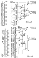
- a miss stack 20 holds the sixteen most recent cache miss addresses, the oldest being identified as address P with entry onto the stack being made at the top.
- Four four-input electronic switches 21, 22, 23, 24 are driven in concert by a shift pattern signal via line 25 such that: in a first state, addresses A, B, C, D appear at to respective outputs of the switches; in a second state, addresses B, D, F, H appear at the outputs; in a third state, addresses C, F, I, L appear at the outputs; and in a fourth state, addresses D, H, L, P appear at the outputs.
- Subtraction circuits 26, 27, 28 are connected to receive as inputs the respective outputs of the electronic switches 21, 22, 23, 24 such that: the output from the subtraction circuit 26 is the output of the switch 21 minus the output of the switch 22; the output from the subtraction circuit 27 is the output of the switch 22 minus the output of the switch 23; and the output from the subtraction circuit 28 is the output of the switch 23 minus the output of the switch 24.
- the output from the subtraction circuit 26 is applied to one input of an adder circuit 31 which has its other input driven by the output of the electronic switch 21.
- the output from the subtraction circuit 26 is also applied to one input of a comparator circuit 29.
- the output from the subtraction circuit 27 is applied to the other input of the comparator circuit 29 and also to one input of another comparator circuit 30 which has its other input driven by the output of the subtraction circuit 28.
- the outputs from the comparator circuits 29, 30 are applied, respectively, to the two inputs of an AND-gate 32 which selectively issues a prefetch enable signal.
- miss stack 20 holds the last sixteen cache miss addresses, address A being the most recent.
- circuit operation is instituted to search for a pattern among the addresses resident in the miss stack.
- the electronic switches 21, 22, 23, 24 are at their first state such that address A is passed through to the output of switch 21, address B appears at the output of switch 22, address C appears at the output of switch 23 and address D appears at the output of switch 24.
- the electronic switches would have been advanced to their next state to examine the address combination CFIL and then on to the address combination DHLP if necessary. If no pattern was sensed, the circuit would await the next cache miss which will place a new entry at the top of the miss stack and push address P out the bottom of the stack before the pattern match search is again instituted.
- Electronic switches 41, 42, 43, 44 receive at their respective inputs recent cache miss addresses as stored in the miss stack 40 in the exemplary arrangement shown. It will be noted that each of the electronic switches 41, 42, 43, 44 has eight inputs which can be sequentially selectively transferred to the single outputs under the influence of the shift pattern signal. It will also be noted that the miss stack 40 stores, in addition to the sixteen latest cache miss addresses A - P, three future entries WXY. Subtraction circuits 45, 46, 47 perform the same office as the corresponding subtraction circuits 26, 27, 28 of the FIG. 3 embodiment previously described. Similarly, adder circuit 48 corresponds to the adder circuit 31 previously described.
- Comparator circuit 49 receives the respective outputs of the subtraction circuits 45, 46, and its output is applied to one input of an AND-gate 38 which selectively issues the prefetch enable signal.
- Comparator circuit 50 receives the respective outputs of the subtraction circuits 46, 47, but, unlike its counterpart comparator 30 of the FIG. 3 embodiment, its output is applied to one input of an OR-gate 39 which has its other input driven by a reduce lookahead signal.
- the output of OR-gate 39 is coupled to the other input of AND-gate 38.
- the effect of applying the reduce lookahead signal is to compare only the outputs of the subtraction circuits 45, 46 in the comparator circuit 49 such that a compare fully enables the AND-gate 38 to issue the prefetch enable signal.
- This mode of operation may be useful, for example, when the patterns seem to be changing every few cache misses, and it favors the most recent examples.
- the goal states are searched in groups by switch state; i.e.: Group 1 includes switch states 0, 1, 2 and could result in filling future entries WXY; Group 2 includes states 3, 4 and could result in filling entries WX; Group 3 includes states 5, 6 and could also result in filling entries WX; and Group 4 includes state 7 and could result in filling entry W.
- switch state i.e.: Group 1 includes switch states 0, 1, 2 and could result in filling future entries WXY; Group 2 includes states 3, 4 and could result in filling entries WX; Group 3 includes states 5, 6 and could also result in filling entries WX; and Group 4 includes state 7 and could result in filling entry W.
- FIGs. 3 and 4 are somewhat simplified since multiple binary digit information is presented as if it were single binary digit information.
- arrays of electronic switches, gates, etc. will actually be employed to handle the added dimension as may be necessary and entirely conventionally.
- timing signals and logic for incorporating the inventive structure into a given data processing system environment will be those appropriate for that environment and will be the subject of straightforward logic design.
Landscapes
- Engineering & Computer Science (AREA)
- Theoretical Computer Science (AREA)
- Software Systems (AREA)
- Physics & Mathematics (AREA)
- General Engineering & Computer Science (AREA)
- General Physics & Mathematics (AREA)
- Memory System Of A Hierarchy Structure (AREA)
Claims (14)
- Verfahren zum Voraussagen von Cache-Anforderungsadressen, um Signalgruppen aus einem Hauptspeicher in einen Cache-Speicher in einem Datenverarbeitungssystem im voraus zu holen, wobei der Cache-Speicher wiederholt abgefragt wird, um zu bestimmen, ob eine Adresse, die einer Cache-Anforderungsadresse entspricht, darin gespeichert ist, wobei das Datenverarbeitungssystem einen Stapelspeicher zum Speichern von Cache-Fehladressen aufweist, wobei das Verfahren den Schritt aufweist:
A) nach Auftreten eines Cache-Verfehlens wird, wenn der Cache-Speicher abgefragt ist, die Cache-Anforderungsadresse, die dem Cache-Verfehlen entspricht, in den Stapelspeicher eingegeben; gekennzeichnet durch die weiteren Schritte:B) Untersuchen der Cache-Anforderungsadressen in dem Stapelspeicher, um zu bestimmen, ob ein Adressmuster durch Untersuchen eines Satzes von Einträgen des Stapelspeichers auf gleiche Unterschiede zwischen den Inhalten aufeinanderfolgender Einträge des Satzes gefunden werden kann, undC)(1) wenn kein Muster in Schritt (B) bestimmt worden ist, Zurückkehren zu Schritt (A), aber(2)(i) wenn ein Muster in Schritt (B) bestimmt worden ist, Erzeugen einer vorhergesagten Cache-Anforderungsadresse basierend auf dem Muster und zumindest einer der Cache-Anforderungsadressen, die in dem Stapel vorhanden sind, wobei die vorhergesagte Cache-Anforderungsadresse auf eine Signalgruppe zeigt, die in dem Hauptspeicher gespeichert ist;(ii) Verwenden der vorhergesagten Cache-Anforderungsadresse, um die Signalgruppe zu erhalten, die durch die vorhergesagte Cache-Anforderungsadresse von dem Hauptspeicher identifiziert ist, und um eine solche Signalgruppe in den Cachespeicher zu schreiben, und(iii) Zurückkehren zu Schritt A). - Verfahren gemäß Anspruch 1, wobei der Stapelspeicher ein First-In-First-Out-Stapelspeicher ist, der weiter dadurch gekennzeichnet ist, daß:
in Schritt (A) die Cache-Anforderungsadresse in den oberen Teil des Stapelspeichers eingetragen wird. - Verfahren gemäß Anspruch 1, wobei in Schritt B) das Adressmuster eines einer Vielzahl von suchbaren vorbestimmten Adressmustern ist.
- Verfahren gemäß Anspruch 3, wobei der Schritt B) des Untersuchens der Cache-Anforderungsadressen, die in dem Stack vorhanden sind, die Schritte aufweist:(B) (1) Auswählen eines derzeit geltenden Adressmusters aus der Vielzahl von Adressmustern;(B) (2) Untersuchen der Cache-Anforderungsadressen, die in dem Stapelspeicher vorhanden sind, auf eine Übereinstimmung mit dem derzeit geltenden Adressmuster;(B) (3) wenn das derzeit geltende Adressmuster nicht mit den Cache-Anforderungsadressen übereinstimmt, die in dem Stapelspeicher vorhanden sind, bestimmen, ob alle der Vielzahl von vorbestimmten Adressmustern untersucht worden sind, und(B) (4) wenn das derzeit geltende Adressmuster nicht mit den Cache-Anforderungsadressen übereinstimmt, die in dem Stapelspeicher vorhanden sind, und nicht alle der vorbestimmten Adressmuster untersucht worden sind, Auswählen eines Adressmusters, das anders als das derzeit geltende Adressmuster ist, das zuvor im Schritt (B) (1) ausgewählt worden ist, als derzeit geltendes Adressmuster und dann Zurückkehren zu Schritt (B) (2).
- Verfahren gemäß Anspruch 4, wobei die Vielzahl von vorbestimmten Adressmustern eine Vielzahl von Mustergruppen aufweist und wobei die Vielzahl von Mustergruppen eine derzeit geltende Mustergruppe aufweist, die das derzeit geltende Adressmuster enthält.
- Verfahren gemäß Anspruch 5, wobei Schritt (B) (4) die Schritte aufweist:(B) (4) (1) Bestimmen, ob alle der Adressmuster in der derzeit geltenden Mustergruppe untersucht worden sind; und(B) (4) (2) wenn nicht alle der Adressmuster in der derzeit geltenden Mustergruppe untersucht worden sind, Auswählen eines Adressmusters, das anders als das derzeit geltende Adressmuster ist, das zuvor ausgewählt worden ist, als das derzeit geltende Adressmuster aus der derzeit geltenden Mustergruppe; und(B) (4) (3) wenn alle der Adressmuster in der derzeit geltenden Mustergruppe untersucht worden sind, Auswählen eines der Adressmuster aus einer anderen Mustergruppe als der derzeit geltenden Mustergruppe als derzeit geltendes Adressmuster.
- Verfahren gemäß Anspruch 6, das weiter die Schritte aufweist:(C) (2) (ii) (a) wenn das derzeit geltende Adressmuster mit den Cache-Anforderungsadressen übereinstimmt, die in dem Stapelspeicher vorhanden sind, Auswählen eines der Adressmuster aus einer anderen Mustergruppe als der zuvor ausgewählten derzeit geltenden Mustergruppe als das derzeit geltende Adressmuster; undC) (2) (ii) (b) wenn es zumindest eine der Mustergruppen gibt, in der keines der vorbestimmten Adressmuster untersucht worden ist, Zurückkehren zu Schritt B).
- Verfahren gemäß Anspruch 1, wobei ein Cache-Verfehlen das Ergebnis des Fehlens von aufgerufener Information in dem Cache-Speicher ist, die von dem Cache-Speicher angefordert worden ist.
- Verfahren gemäß Anspruch 1, wobei Schritt C) (2) weiter den Schritt aufweist, die vorhergesagte Cache-Anforderungsadresse oben in dem Stapelspeicher zu plazieren.
- Vorrichtung zum Erzeugen einer vorhergesagten Cache-Anforderungsadresse, um Signalgruppen im voraus aus einem Hauptspeicher in einen Cache-Speicher in einem Datenverarbeitungssystem zu holen, in dem dessen Cache-Speicher wiederholt abgefragt wird, um zu bestimmen, ob eine Adresse, die einer Cache-Anforderungsadresse entspricht, darin gespeichert ist, wobei die gespeicherte Adresse Information entspricht, die auch in dem Cache-Speicher gespeichert ist;wobei das Datenverarbeitungssystem einen Speicher (20) zum Halten einer Vielzahl von Cache-Anforderungsadressen in jeweiligen Zellen davon aufweist;wobei die Vorrichtung gekennzeichnet ist, durch:eine Vielzahl von Schaltern (21-24; 41-44), wobei jeder der Schalter (21-24; 41-44) eine Vielzahl von Eingangsanschlußklemmen, eine Ausgangsanschlußklemme und eine Steueranschlußklemme aufweist, so daß ein Steuersignal, das an die Steueranschlußklemme angelegt wird, veranlaßt, daß der Schalter eine der Eingangsanschlußklemmen mit der Ausgangsklemme koppelt; wobei das Steuersignal zu den Steueranschlußklemmen geliefert wird, um die Eingangsanschlußklemmen der Schalter (21-24; 41-44) dazu zu veranlassen, sukzessiv an die Ausgangsanschlußklemme gekoppelt zu werden;eine Schaltung zum Koppeln jeder der Eingangsanschlußklemmen der Schalter (21-24; 41-44) an eine der Zellen;eine Vielzahl von ersten arithmetischen Schaltungen (26-28; 45-47), wobei jede der ersten arithmetischen Schaltungen (26-28; 45-47) ein Paar Einganesanschlußklemmen und eine Ausgangsanschlußklemme aufweist, wobei die Eingangsanschlußklemmen jeder der ersten arithmetischen Schaltungen (26-28; 45-47) an die jeweiligen Ausgangsanschlußklemmen von zwei der Schalter (21-24; 41-44) gekoppelt sind, wobei jede der ersten arithmetischen Schaltungen (26-28; 45-47) eine arithmetische Operation auf den beiden Cache-Anforderungsadressen durchführt, die durch ihre Eingangsanschlußklemmen von den beiden Zellen des Speichers empfangen worden sind, der an die Eingangsanschlußklemmen durch die beiden Schalter gekoppelt ist, und ein Signal an ihre Ausgangsanschlußklemme liefert, das das Ergebnis der arithmetischen Operation darstellt;eine Vielzahl von Komparatoren (29, 30; 49, 50), wobei jeder der Komparatoren (29, 30; 49, 50) ein Paar Eingangsanschlußklemmen und eine Ausgangsanschlußklemme aufweist, wobei die Eingangsanschlußklemmen jedes der Komparatoren (29, 30; 49, 50) an die jeweiligen Ausgangsanschlußklemmen von zwei der ersten arithmetischen Schaltungen (26-28; 45-47) gekoppelt sind, wobei jeder der beiden Komparatoren (29, 30; 49, 50) die beiden arithmetischen Ergebnissignale, die dadurch empfangen worden sind, vergleicht, und ein Signal an seiner Ausgangsanschlußklemme liefert, das anzeigt, ob die Ergebnissignale ähnlich sind;eine zweite arithmetische Schaltung (31), die ein Paar Eingangsanschlußklemmen und eine Ausgangsanschlußklemme aufweist, wobei eine erste Eingangsanschlußklemme der zweiten arithmetischen Schaltung (31) an die Ausgangsanschlußklemme eines der Schalter (21-24; 41-44) gekoppelt ist, und wobei die zweite Eingangsanschlußklemme der zweiten arithmetischen Schaltung (31) an die Ausgangsanschlußklemme einer der ersten arithmetischen Schaltungen (26-28; 45-47) gekoppelt ist, wobei die zweite arithmetische Schaltung (31) eine arithmetische Operation auf der Anforderunesadresse, die durch die erste Eingangsanschlußklemme empfangen worden ist, und dem arithmetischen Ergebnis durchführt, das durch das Signal dargestellt ist, das durch die zweiten Eingangsanschlußklemmen empfangen worden ist, und ein Ausgangssignal an seine Ausgangsanschlußklemme liefert, das das Ergebnis der arithmetischen Operation anzeigt, die durch die zweite arithmetische Schaltung (31) durchgeführt worden ist;wodurch, wenn die Signale, die an die Ausgangsanschlußklemmen aller Komparatoren (29, 30; 49, 50) geliefert worden sind, anzeigen, daß die verglichenen arithmetischen Ergebnisse ähnlich sind, das arithmetische Ergebnis, das durch die konkurrienden Ausgangssignale der zweiten arithmetischen Schaltung (31) dargestellt wird, die vorhergesagte Cache-Anforderungsadresse darstellt.
- Vorrichtung gemäß Anspruch 10, wobei die Vielzahl von ersten arithmetischen Schaltungen (26-28; 45-47) eine Vielzahl von Subtraktionsschaltungen aufweist, wobei jede der Subtraktionsschaltungen zum Erzeugen eines Wertes dient, der eine Verschiebung zwischen zwei Cache-Anforderungsadressen darstellt.
- Vorrichtung gemäß Anspruch 11, die weiter ein erstes logisches Gatter (32; 38) mit einer Vielzahl von Eingängen aufweist, die getrennt an die Eingangsanschlußklemmen von zumindest zwei der Komparatoren (29, 30; 49, 50) gekoppelt sind, um selektiv ein Prefetch-Freigabesignal auszugeben, wenn das erste logische Gatter (32; 38) vollständig freigegeben ist.
- Vorrichtung gemäß Anspruch 12, die weiter ein zweites logisches Gatter (39) aufweist, das zumindest einen der Eingängen des ersten logischen Gatters (38) antreibt, wobei das zweite logische Gatter (39) Eingänge hat, die gekoppelt sind, um die Ausgabe von zumindest einer der Komparatorschaltungen (49, 50) zu empfangen, und ein selektiv angelegtes Reduktions-Lookahead-Logiksignal aufweist, so daß das Anlegen des Reduktions-Lookahead-Logiksignales an das zweite logische Gatter (39) teilweise das erste Logikgatter (38) freigibt und dadurch zumindest eine der Komparatorschaltungen (49, 50) von der Betrachtung beim Ausgeben des Prefetch-Freigabe-Logiksignales eliminiert.
- Vorrichtung gemäß Anspruch 13, wobei das erste logische Gatter (32; 38) ein AND-Gatter ist und wobei das zweite logische Gatter (39) ein OR-Gatter ist.
Applications Claiming Priority (2)
| Application Number | Priority Date | Filing Date | Title |
|---|---|---|---|
| US364943 | 1989-06-12 | ||
| US07/364,943 US5093777A (en) | 1989-06-12 | 1989-06-12 | Method and apparatus for predicting address of a subsequent cache request upon analyzing address patterns stored in separate miss stack |
Publications (3)
| Publication Number | Publication Date |
|---|---|
| EP0402787A2 EP0402787A2 (de) | 1990-12-19 |
| EP0402787A3 EP0402787A3 (de) | 1991-09-04 |
| EP0402787B1 true EP0402787B1 (de) | 1996-08-21 |
Family
ID=23436798
Family Applications (1)
| Application Number | Title | Priority Date | Filing Date |
|---|---|---|---|
| EP90110881A Expired - Lifetime EP0402787B1 (de) | 1989-06-12 | 1990-06-08 | Cache-Speicherfehlgriffsvorhersageverfahren und -vorrichtung |
Country Status (7)
| Country | Link |
|---|---|
| US (2) | US5093777A (de) |
| EP (1) | EP0402787B1 (de) |
| JP (1) | JPH0363852A (de) |
| KR (1) | KR950011291B1 (de) |
| AU (1) | AU638716B2 (de) |
| DE (1) | DE69028153T2 (de) |
| SG (1) | SG49211A1 (de) |
Families Citing this family (67)
| Publication number | Priority date | Publication date | Assignee | Title |
|---|---|---|---|---|
| US5093777A (en) * | 1989-06-12 | 1992-03-03 | Bull Hn Information Systems Inc. | Method and apparatus for predicting address of a subsequent cache request upon analyzing address patterns stored in separate miss stack |
| US5210838A (en) * | 1990-05-15 | 1993-05-11 | Sun Microsystems, Inc. | Method and apparatus for predicting the effective addresses of future memory load operations in a microprocessor |
| GB2247546B (en) * | 1990-08-31 | 1995-03-01 | Sun Microsystems Inc | Method and apparatus for predictive caching |
| US5357618A (en) * | 1991-04-15 | 1994-10-18 | International Business Machines Corporation | Cache prefetch and bypass using stride registers |
| SE469402B (sv) * | 1991-05-02 | 1993-06-28 | Swedish Inst Of Computer Scien | Foerfarande foer att haemta data till ett cache-minne |
| US5367656A (en) * | 1992-03-13 | 1994-11-22 | Bull Hn Information Systems Inc. | Controlling cache predictive prefetching based on cache hit ratio trend |
| US5787475A (en) * | 1992-07-21 | 1998-07-28 | Digital Equipment Corporation | Controlled prefetching of data requested by a peripheral |
| US5450561A (en) * | 1992-07-29 | 1995-09-12 | Bull Hn Information Systems Inc. | Cache miss prediction method and apparatus for use with a paged main memory in a data processing system |
| US5715421A (en) * | 1992-10-16 | 1998-02-03 | Seiko Epson Corporation | Apparatus and method of addressing paged mode memory including adjacent page precharging |
| US5588128A (en) * | 1993-04-02 | 1996-12-24 | Vlsi Technology, Inc. | Dynamic direction look ahead read buffer |
| WO1995001600A1 (en) * | 1993-07-02 | 1995-01-12 | Oakleigh Systems, Inc. | Predictive disk cache system |
| US5452440A (en) * | 1993-07-16 | 1995-09-19 | Zitel Corporation | Method and structure for evaluating and enhancing the performance of cache memory systems |
| US5426764A (en) * | 1993-08-24 | 1995-06-20 | Ryan; Charles P. | Cache miss prediction apparatus with priority encoder for multiple prediction matches and method therefor |
| US5701426A (en) * | 1995-03-31 | 1997-12-23 | Bull Information Systems Inc. | Data processing system and method using cache miss address prediction and forced LRU status in a cache memory to improve cache hit ratio |
| US5790823A (en) * | 1995-07-13 | 1998-08-04 | International Business Machines Corporation | Operand prefetch table |
| US6038643A (en) * | 1996-01-24 | 2000-03-14 | Sun Microsystems, Inc. | Stack management unit and method for a processor having a stack |
| KR100584964B1 (ko) * | 1996-01-24 | 2006-05-29 | 선 마이크로시스템즈 인코퍼레이티드 | 스택 메모리 구조에서의 캐싱 장치 |
| US6055621A (en) * | 1996-02-12 | 2000-04-25 | International Business Machines Corporation | Touch history table |
| US5854911A (en) * | 1996-07-01 | 1998-12-29 | Sun Microsystems, Inc. | Data buffer prefetch apparatus and method |
| US6167488A (en) * | 1997-03-31 | 2000-12-26 | Sun Microsystems, Inc. | Stack caching circuit with overflow/underflow unit |
| US6009499A (en) * | 1997-03-31 | 1999-12-28 | Sun Microsystems, Inc | Pipelined stack caching circuit |
| US6289418B1 (en) | 1997-03-31 | 2001-09-11 | Sun Microsystems, Inc. | Address pipelined stack caching method |
| US6131144A (en) * | 1997-04-01 | 2000-10-10 | Sun Microsystems, Inc. | Stack caching method with overflow/underflow control using pointers |
| JP3175675B2 (ja) * | 1997-12-04 | 2001-06-11 | 日本電気株式会社 | プリフェッチ制御装置 |
| US6058457A (en) * | 1997-06-23 | 2000-05-02 | Sun Microsystems, Inc. | Method for storing method frames in multiple stacks |
| US6092152A (en) * | 1997-06-23 | 2000-07-18 | Sun Microsystems, Inc. | Method for stack-caching method frames |
| US6067602A (en) * | 1997-06-23 | 2000-05-23 | Sun Microsystems, Inc. | Multi-stack-caching memory architecture |
| US6138210A (en) * | 1997-06-23 | 2000-10-24 | Sun Microsystems, Inc. | Multi-stack memory architecture |
| US6197685B1 (en) * | 1997-07-11 | 2001-03-06 | Matsushita Electronics Corporation | Method of producing multilayer wiring device with offset axises of upper and lower plugs |
| US6047363A (en) * | 1997-10-14 | 2000-04-04 | Advanced Micro Devices, Inc. | Prefetching data using profile of cache misses from earlier code executions |
| US6134643A (en) * | 1997-11-26 | 2000-10-17 | Intel Corporation | Method and apparatus for cache line prediction and prefetching using a prefetch controller and buffer and access history |
| US6484239B1 (en) * | 1997-12-29 | 2002-11-19 | Intel Corporation | Prefetch queue |
| US6108768A (en) * | 1998-04-22 | 2000-08-22 | Sun Microsystems, Inc. | Reissue logic for individually reissuing instructions trapped in a multiissue stack based computing system |
| US6170050B1 (en) | 1998-04-22 | 2001-01-02 | Sun Microsystems, Inc. | Length decoder for variable length data |
| US6275903B1 (en) | 1998-04-22 | 2001-08-14 | Sun Microsystems, Inc. | Stack cache miss handling |
| US6237086B1 (en) | 1998-04-22 | 2001-05-22 | Sun Microsystems, Inc. | 1 Method to prevent pipeline stalls in superscalar stack based computing systems |
| US6230260B1 (en) | 1998-09-01 | 2001-05-08 | International Business Machines Corporation | Circuit arrangement and method of speculative instruction execution utilizing instruction history caching |
| US7020879B1 (en) * | 1998-12-16 | 2006-03-28 | Mips Technologies, Inc. | Interrupt and exception handling for multi-streaming digital processors |
| US7237093B1 (en) * | 1998-12-16 | 2007-06-26 | Mips Technologies, Inc. | Instruction fetching system in a multithreaded processor utilizing cache miss predictions to fetch instructions from multiple hardware streams |
| US7529907B2 (en) | 1998-12-16 | 2009-05-05 | Mips Technologies, Inc. | Method and apparatus for improved computer load and store operations |
| US6389449B1 (en) * | 1998-12-16 | 2002-05-14 | Clearwater Networks, Inc. | Interstream control and communications for multi-streaming digital processors |
| US7257814B1 (en) | 1998-12-16 | 2007-08-14 | Mips Technologies, Inc. | Method and apparatus for implementing atomicity of memory operations in dynamic multi-streaming processors |
| US7035997B1 (en) | 1998-12-16 | 2006-04-25 | Mips Technologies, Inc. | Methods and apparatus for improving fetching and dispatch of instructions in multithreaded processors |
| US6393527B1 (en) * | 1998-12-18 | 2002-05-21 | Ati International Srl | Prefetch buffer with continue detect |
| US6490652B1 (en) * | 1999-02-03 | 2002-12-03 | Ati Technologies Inc. | Method and apparatus for decoupled retrieval of cache miss data |
| US6311260B1 (en) | 1999-02-25 | 2001-10-30 | Nec Research Institute, Inc. | Method for perfetching structured data |
| US20020135611A1 (en) * | 1999-03-04 | 2002-09-26 | Trevor Deosaran | Remote performance management to accelerate distributed processes |
| US6580431B1 (en) | 1999-03-04 | 2003-06-17 | Nexmem | System, method, and computer program product for intelligent memory to accelerate processes |
| JP3438650B2 (ja) * | 1999-05-26 | 2003-08-18 | 日本電気株式会社 | キャッシュメモリ |
| US6442673B1 (en) * | 1999-11-05 | 2002-08-27 | I.P. First L.L.C. | Update forwarding cache for address mode |
| US6629234B1 (en) | 2000-03-30 | 2003-09-30 | Ip. First, L.L.C. | Speculative generation at address generation stage of previous instruction result stored in forward cache for use by succeeding address dependent instruction |
| JP2004518183A (ja) | 2000-07-14 | 2004-06-17 | クリアウオーター・ネツトワークス・インコーポレイテツド | マルチスレッド・システムにおける命令のフェッチとディスパッチ |
| US6584549B2 (en) | 2000-12-29 | 2003-06-24 | Intel Corporation | System and method for prefetching data into a cache based on miss distance |
| US7035979B2 (en) * | 2002-05-22 | 2006-04-25 | International Business Machines Corporation | Method and apparatus for optimizing cache hit ratio in non L1 caches |
| US7107438B2 (en) | 2003-02-04 | 2006-09-12 | Via Technologies, Inc. | Pipelined microprocessor, apparatus, and method for performing early correction of conditional branch instruction mispredictions |
| US7185182B2 (en) | 2003-02-04 | 2007-02-27 | Via Technologies, Inc. | Pipelined microprocessor, apparatus, and method for generating early instruction results |
| US7100024B2 (en) | 2003-02-04 | 2006-08-29 | Via Technologies, Inc. | Pipelined microprocessor, apparatus, and method for generating early status flags |
| US8966230B2 (en) | 2009-09-30 | 2015-02-24 | Intel Corporation | Dynamic selection of execution stage |
| CN102163144A (zh) * | 2011-05-05 | 2011-08-24 | 浙江大学 | 嵌入式处理器的硬件数据预取方法 |
| US8954678B2 (en) * | 2012-06-15 | 2015-02-10 | International Business Machines Corporation | Automatic pattern-based operand prefetching |
| US9015422B2 (en) * | 2013-07-16 | 2015-04-21 | Apple Inc. | Access map-pattern match based prefetch unit for a processor |
| US10360159B1 (en) | 2013-12-12 | 2019-07-23 | Groupon, Inc. | System, method, apparatus, and computer program product for providing a cache mechanism |
| US9971694B1 (en) | 2015-06-24 | 2018-05-15 | Apple Inc. | Prefetch circuit for a processor with pointer optimization |
| KR102429903B1 (ko) * | 2015-12-03 | 2022-08-05 | 삼성전자주식회사 | 비휘발성 메인 메모리 시스템의 페이지 폴트 처리 방법 |
| US10180905B1 (en) | 2016-04-07 | 2019-01-15 | Apple Inc. | Unified prefetch circuit for multi-level caches |
| US9904624B1 (en) | 2016-04-07 | 2018-02-27 | Apple Inc. | Prefetch throttling in a multi-core system |
| US10331567B1 (en) | 2017-02-17 | 2019-06-25 | Apple Inc. | Prefetch circuit with global quality factor to reduce aggressiveness in low power modes |
Family Cites Families (16)
| Publication number | Priority date | Publication date | Assignee | Title |
|---|---|---|---|---|
| GB1515376A (en) * | 1975-07-09 | 1978-06-21 | Int Computers Ltd | Data storage systems |
| US4371924A (en) * | 1979-11-09 | 1983-02-01 | Rockwell International Corp. | Computer system apparatus for prefetching data requested by a peripheral device from memory |
| US4317168A (en) * | 1979-11-23 | 1982-02-23 | International Business Machines Corporation | Cache organization enabling concurrent line castout and line fetch transfers with main storage |
| US4370710A (en) * | 1980-08-26 | 1983-01-25 | Control Data Corporation | Cache memory organization utilizing miss information holding registers to prevent lockup from cache misses |
| US4583165A (en) * | 1982-06-30 | 1986-04-15 | International Business Machines Corporation | Apparatus and method for controlling storage access in a multilevel storage system |
| US4679141A (en) * | 1985-04-29 | 1987-07-07 | International Business Machines Corporation | Pageable branch history table |
| IT1202687B (it) * | 1987-03-25 | 1989-02-09 | Honeywell Inf Systems | Memoria tampone a predizione di hit |
| US4991090A (en) * | 1987-05-18 | 1991-02-05 | International Business Machines Corporation | Posting out-of-sequence fetches |
| US4980823A (en) * | 1987-06-22 | 1990-12-25 | International Business Machines Corporation | Sequential prefetching with deconfirmation |
| US4943908A (en) * | 1987-12-02 | 1990-07-24 | International Business Machines Corporation | Multiple branch analyzer for prefetching cache lines |
| US4888679A (en) * | 1988-01-11 | 1989-12-19 | Digital Equipment Corporation | Method and apparatus using a cache and main memory for both vector processing and scalar processing by prefetching cache blocks including vector data elements |
| US5093777A (en) * | 1989-06-12 | 1992-03-03 | Bull Hn Information Systems Inc. | Method and apparatus for predicting address of a subsequent cache request upon analyzing address patterns stored in separate miss stack |
| US5269013A (en) * | 1991-03-20 | 1993-12-07 | Digital Equipment Corporation | Adaptive memory management method for coupled memory multiprocessor systems |
| US5185861A (en) * | 1991-08-19 | 1993-02-09 | Sequent Computer Systems, Inc. | Cache affinity scheduler |
| US5305389A (en) * | 1991-08-30 | 1994-04-19 | Digital Equipment Corporation | Predictive cache system |
| US5367656A (en) * | 1992-03-13 | 1994-11-22 | Bull Hn Information Systems Inc. | Controlling cache predictive prefetching based on cache hit ratio trend |
-
1989
- 1989-06-12 US US07/364,943 patent/US5093777A/en not_active Expired - Lifetime
-
1990
- 1990-06-05 AU AU56819/90A patent/AU638716B2/en not_active Ceased
- 1990-06-08 EP EP90110881A patent/EP0402787B1/de not_active Expired - Lifetime
- 1990-06-08 SG SG1996007658A patent/SG49211A1/en unknown
- 1990-06-08 DE DE69028153T patent/DE69028153T2/de not_active Expired - Fee Related
- 1990-06-09 KR KR1019900008452A patent/KR950011291B1/ko not_active Expired - Fee Related
- 1990-06-12 JP JP2153812A patent/JPH0363852A/ja active Granted
-
1992
- 1992-02-26 US US07/841,687 patent/US5694572A/en not_active Expired - Lifetime
Also Published As
| Publication number | Publication date |
|---|---|
| KR950011291B1 (ko) | 1995-09-30 |
| DE69028153D1 (de) | 1996-09-26 |
| KR910001547A (ko) | 1991-01-31 |
| EP0402787A2 (de) | 1990-12-19 |
| SG49211A1 (en) | 1998-05-18 |
| JPH0363852A (ja) | 1991-03-19 |
| DE69028153T2 (de) | 1997-04-03 |
| JPH0529939B2 (de) | 1993-05-06 |
| US5694572A (en) | 1997-12-02 |
| AU638716B2 (en) | 1993-07-08 |
| EP0402787A3 (de) | 1991-09-04 |
| US5093777A (en) | 1992-03-03 |
| AU5681990A (en) | 1990-12-13 |
Similar Documents
| Publication | Publication Date | Title |
|---|---|---|
| EP0402787B1 (de) | Cache-Speicherfehlgriffsvorhersageverfahren und -vorrichtung | |
| EP0560100B1 (de) | Adaptiver Cache-Speicherfehlgriffvorhersagemechanismus | |
| US4980823A (en) | Sequential prefetching with deconfirmation | |
| US5701426A (en) | Data processing system and method using cache miss address prediction and forced LRU status in a cache memory to improve cache hit ratio | |
| US5450561A (en) | Cache miss prediction method and apparatus for use with a paged main memory in a data processing system | |
| EP0348495B1 (de) | Methode und digitaler computer zum vorausholen von vektordaten aus dem speicher in einem für skalaverarbeitung bestimmten speichersystem | |
| US5091851A (en) | Fast multiple-word accesses from a multi-way set-associative cache memory | |
| US4604691A (en) | Data processing system having branch instruction prefetching performance | |
| EP0097790B1 (de) | Gerät zur Speicherzugriffssteuerung in einer mehrstufigen Speicheranordnung | |
| JPS6118222B2 (de) | ||
| JPH11504458A (ja) | スーパースカラマイクロプロセッサにおける分岐予測正確度向上のための装置および方法 | |
| JP3254019B2 (ja) | データ先読み制御装置 | |
| KR100618248B1 (ko) | 실행 엔진으로부터 다중 데이터 소스까지 다중 로드 및 기억 요구를 지원하는 장치 및 방법 | |
| US5495591A (en) | Method and system for cache miss prediction based on previous cache access requests | |
| US5426764A (en) | Cache miss prediction apparatus with priority encoder for multiple prediction matches and method therefor | |
| US5283890A (en) | Cache memory arrangement with write buffer pipeline providing for concurrent cache determinations | |
| US5276853A (en) | Cache system | |
| CN115587052A (zh) | 一种缓存性能的处理方法及其相关设备 | |
| JPH0477344B2 (de) | ||
| JP3284508B2 (ja) | データ先読み制御装置 | |
| JP3697990B2 (ja) | ベクトル処理装置のオペランドキャッシュ | |
| EP0101759B1 (de) | Datenverarbeitungssystem mit Sprunginstruktionsvorgriff | |
| JPH0690681B2 (ja) | キャッシュメモリ制御方式 | |
| JPS6161143B2 (de) | ||
| JPH03116345A (ja) | データ処理装置 |
Legal Events
| Date | Code | Title | Description |
|---|---|---|---|
| PUAI | Public reference made under article 153(3) epc to a published international application that has entered the european phase |
Free format text: ORIGINAL CODE: 0009012 |
|
| AK | Designated contracting states |
Kind code of ref document: A2 Designated state(s): DE FR GB IT |
|
| PUAL | Search report despatched |
Free format text: ORIGINAL CODE: 0009013 |
|
| AK | Designated contracting states |
Kind code of ref document: A3 Designated state(s): DE FR GB IT |
|
| 17P | Request for examination filed |
Effective date: 19920226 |
|
| RAP1 | Party data changed (applicant data changed or rights of an application transferred) |
Owner name: INTEL CORPORATION |
|
| 17Q | First examination report despatched |
Effective date: 19950111 |
|
| GRAH | Despatch of communication of intention to grant a patent |
Free format text: ORIGINAL CODE: EPIDOS IGRA |
|
| GRAA | (expected) grant |
Free format text: ORIGINAL CODE: 0009210 |
|
| GRAH | Despatch of communication of intention to grant a patent |
Free format text: ORIGINAL CODE: EPIDOS IGRA |
|
| AK | Designated contracting states |
Kind code of ref document: B1 Designated state(s): DE FR GB IT |
|
| ITF | It: translation for a ep patent filed | ||
| REF | Corresponds to: |
Ref document number: 69028153 Country of ref document: DE Date of ref document: 19960926 |
|
| ET | Fr: translation filed | ||
| PLBE | No opposition filed within time limit |
Free format text: ORIGINAL CODE: 0009261 |
|
| STAA | Information on the status of an ep patent application or granted ep patent |
Free format text: STATUS: NO OPPOSITION FILED WITHIN TIME LIMIT |
|
| 26N | No opposition filed | ||
| PGFP | Annual fee paid to national office [announced via postgrant information from national office to epo] |
Ref country code: FR Payment date: 20000517 Year of fee payment: 11 |
|
| PGFP | Annual fee paid to national office [announced via postgrant information from national office to epo] |
Ref country code: DE Payment date: 20000518 Year of fee payment: 11 |
|
| PGFP | Annual fee paid to national office [announced via postgrant information from national office to epo] |
Ref country code: GB Payment date: 20000519 Year of fee payment: 11 |
|
| PG25 | Lapsed in a contracting state [announced via postgrant information from national office to epo] |
Ref country code: GB Free format text: LAPSE BECAUSE OF NON-PAYMENT OF DUE FEES Effective date: 20010608 |
|
| GBPC | Gb: european patent ceased through non-payment of renewal fee |
Effective date: 20010608 |
|
| PG25 | Lapsed in a contracting state [announced via postgrant information from national office to epo] |
Ref country code: FR Free format text: LAPSE BECAUSE OF NON-PAYMENT OF DUE FEES Effective date: 20020228 |
|
| PG25 | Lapsed in a contracting state [announced via postgrant information from national office to epo] |
Ref country code: DE Free format text: LAPSE BECAUSE OF NON-PAYMENT OF DUE FEES Effective date: 20020403 |
|
| PG25 | Lapsed in a contracting state [announced via postgrant information from national office to epo] |
Ref country code: IT Free format text: LAPSE BECAUSE OF NON-PAYMENT OF DUE FEES Effective date: 20050608 |