EP0392397A2 - Symbolbreite elastische Puffereinrichtung - Google Patents
Symbolbreite elastische Puffereinrichtung Download PDFInfo
- Publication number
- EP0392397A2 EP0392397A2 EP90106672A EP90106672A EP0392397A2 EP 0392397 A2 EP0392397 A2 EP 0392397A2 EP 90106672 A EP90106672 A EP 90106672A EP 90106672 A EP90106672 A EP 90106672A EP 0392397 A2 EP0392397 A2 EP 0392397A2
- Authority
- EP
- European Patent Office
- Prior art keywords
- section
- symbols
- read
- elasticity buffer
- signal
- Prior art date
- Legal status (The legal status is an assumption and is not a legal conclusion. Google has not performed a legal analysis and makes no representation as to the accuracy of the status listed.)
- Withdrawn
Links
Images



Classifications
-
- H—ELECTRICITY
- H04—ELECTRIC COMMUNICATION TECHNIQUE
- H04J—MULTIPLEX COMMUNICATION
- H04J3/00—Time-division multiplex systems
- H04J3/02—Details
- H04J3/06—Synchronising arrangements
-
- H—ELECTRICITY
- H04—ELECTRIC COMMUNICATION TECHNIQUE
- H04J—MULTIPLEX COMMUNICATION
- H04J3/00—Time-division multiplex systems
- H04J3/02—Details
- H04J3/06—Synchronising arrangements
- H04J3/062—Synchronisation of signals having the same nominal but fluctuating bit rates, e.g. using buffers
- H04J3/0632—Synchronisation of packets and cells, e.g. transmission of voice via a packet network, circuit emulation service [CES]
Definitions
- the present invention relates to digital data communications systems and, in particular, to an elasticity buffer that accommodates frequency differences between the receive clock and the local transmit clock in a data terminal while permitting timing drift between terminal clocks and maintaining constant timing between data packets.
- each data terminal within the system receives incoming data from a transmitting station based upon a "receive" clock which is recovered from the incoming signal.
- the receiving terminal relies upon an asynchronous "local” clock to retransmit the data recovered from the incoming signal.
- Network synchronization is maintained by utilizing an elasticity buffer to compensate for the phase and frequency differences between the recovered receive clock and the local transmit clock.
- Asynchronous data terminals transmit a contiguous series, or packet, of data characters which are separated by start-stop code patterns.
- start delimiter a unique start code
- end delimiter a unique stop code
- the recovery timing of the receiving terminal must be the same as or very close to the transmission timing of the transmitting terminal in order to achieve reliable data packet propagation. If there is a timing difference between the transmitting terminal and the receiving terminal, then receiver data sampling will drift, causing eventual data sampling error at the limits of the data packets and, hence, system malfunctioning.
- metastability problems can be created by the phase differential between a data terminal's recovered write (receive) clock and local read (transmit) clock. If the read and write clock speeds are high in comparison to the intrinsic speed of the terminal's logic circuits, then a metastable state between logic "1" and "0" can persist and be propagated to the transmitted data.
- An obvious solution to this problem is to build faster logic.
- Another solution is to create a chain of latches to allow the metastability to settle out; this solution, however, introduces undesirable delay into the system.
- the Fiber Distributed Data Interface (FDDI) protocol is an ANSI (American National Standards Institute) data transmission standard which applies to a 100 MBit per second token ring network that utilizes an optical fiber transmission medium.
- the FDDI protocol is intended as a high performance interconnection among mainframe computers as well as among mainframes and their associated mass storage subsystems and other peripheral equipment.
- each terminal on the ring must transmit with its own local clock ("jitter" is the short term variation of the transition edges of a digital signal from their ideal positions).
- this local clock is allowed to have a maximum frequency variation of only ⁇ 50PPM from the transmit clock frequency of other data terminals in the system at a transmission rate of 125 Mbits per second. Because the transmitted data are encoded according to a 4B/5B scheme, that is, 4 bits of data are encoded to create a 5 bit symbol, the 125 MBit per second FDDI transmission rate translates to a 100 MBit per second data rate.
- an elasticity buffer be utilized in each terminal.
- the recovered receive clock writes data into the elasticity buffer and the local transmit clock reads the data from the elasticity buffer in a sequential fashion for further transmission.
- an elasticity buffer is a cyclic buffer queue, that is, a series of sequentially accessed storage registers wherein access for a particular operation, i.e. write or read, returns or "wraps around" to the first register in the series after the last register in the series has been accessed for that operation.
- Write pointer logic typically an incrementing counter, holds the address of the register currently accessed for a write operation.
- read pointer logic holds the address of the register currently being accessed for a read operation.
- the elasticity buffer's write pointer starts writing received symbols into the storage registers of the elasticity buffer upon receiving a start delimiter symbol and stops writing symbols after an end delimiter symbol has been written.
- the elasticity buffer's read pointer starts reading symbols from the storage registers upon receiving a read-start signal and stops reading symbols after reading an end delimiter symbol.
- a major limitation of the conventional elasticity buffer design is its requirement that a time gap of at least one symbol or more exist between sequential data packets. That is, a conventional elasticity buffer cannot handle back-to-back data packets with no separation. Since there is no predetermined start area for the second and subsequent back-to-back data packets, both the write and the read pointer logic must "remember" their previous positions. Furthermore, a conventional elasticity buffer cannot function with a continuous stream of line state symbols which contains neither a start delimiter nor an end delimiter.
- a preferred embodiment of a symbol-wide elasticity buffer in accordance with the present invention provides both for reframing, i.e. read/write pointer resynchronization, after each packet and for handling a continuous stream of line state symbols for a period longer than the allowed packet size without resulting in an overflow or underflow condition.
- the elasticity buffer may be divided into two distinct sections, a START section and a CONTINUATION section.
- the buffer's write pointer will not enter the CONTINUATION section, which constitutes a cyclic queue, until the read pointer is directed to the first of the multiple, sequential registers included in the START section.
- the read pointer must then seguentially read each of the START section registers before entering the CONTINUATION section. Once the write pointer or the read pointer has left the START section, it can only reenter upon receipt of a START delimiter signal. When the write pointer or read pointer reaches the last register in the multiple register CONTINUATION section, it is automatically routed back to the first register in the CONTINUATION section.
- a repeat flag may be associated with the last register in the CONTINUATION section.
- the repeat flag is set upon receipt of a repeatable control signal by the write pointer at the last register in the CONTINUATION section .
- the read pointer reaches the final register in the CONTINUATION section and continues to read the same symbol without causing an overflow or underflow.
- the repeat flag is cleared, a CONTINUE signal is generated and the write pointer begins writing to the CONTINUATION section. After a predetermined delay, the read pointer begins reading the first register in the CONTINUATION section.
- the particular embodiment of an elasticity buffer design disclosed herein provides a number of advantages over conventional elasticity buffer designs.
- the length of the START register determines the maximum separation of the read pointer and the write pointer.
- the FDDI protocol defines sixteen data symbols and eight control symbols.
- the eight control symbols are as follows: J, K, Idle, Halt, Quiet, Ending Delimiter, Set and Reset.
- a line state is defined as a continuous stream of a control symbol.
- Idle Line State Idle Line State
- QLS Quiet Line State
- HLS Halt Line State
- MLS Master Line State
- the symbol set for the FDDI protocol is provided in Table I below.
- the external symbol codes are defined by the FDDI standard.
- these codes are decoded to the internal symbol codes by a decoder of conventional design (e.g. a ROM lookup table).
- the internal codes are then written into the elasticity buffer.
- Fig. 1 provides a schematic representation of an elasticity buffer 10 in accordance with the present invention.
- Fig. 4 provides a more detailed circuit diagram of elasticity buffer 10.
- elasticity buffer 10 is divided into a START section and a CONTINUATION section.
- the START section contains five registers; INV, J, K/K1, A and B.
- Each of the START section registers is five bits wide, that is, the width of one internal symbol code.
- the INV register contains a read-only invalid symbol.
- the J register contains a read-only J symbol.
- the K register contains read-only first four bits of the K symbol; K1 contains the remaining writable bit of the K symbol.
- the A and B registers are read-write registers.
- the C, D, E, F, G and H registers constitute the CONTINUATION section, i.e. the actual cyclic queue portion, of the elasticity buffer 10.
- a Repeat Flag (R) is associated with the final (H) register in the CONTINUATION section.
- the write pointer of elasticity buffer 10 Upon power up of the data terminal of which the elasticity buffer 10 is a part, the write pointer of elasticity buffer 10 is cleared and its read pointer is set to the START section's INV register which, as stated above, contains an invalid symbol. Thus, continuous invalid symbols are generated, indicating that the terminal is not receiving data. As will be explained in greater detail below, the only way to exit this mode is by asserting either a START or CONTINUE signal from the terminal's receiver state machine, which resides in front of the elasticity buffer 10.
- a START pulse is generated. As shown in Fig. 1, this causes the write pointer to simultaneously write to the K1 bit of the K register and to the A register.
- K1 bit of the K register By allowing a write to the last bit (K1) of the K register, a START delimiter for a data packet is easily distinguished from that for circuit-switched data as defined in the proposed Hybrid Ring Control extension to the FDDI standard.
- the write pointer of elasticity buffer 10 is synchronized to a receive clock that is recovered from the received data signal, while its read pointer is synchronized to its own local clock, typically a crystal oscillator, the START signal must be resynchronized to the local clock within an acceptable probability that metastability will be avoided.
- two master/slave D latches 12 and 14 are used for this purpose. This results in the creation of a subsequent uncertainty window for the occurrence of a synchronized START signal SYN.START of between one-half (1 ⁇ 2) and one and one-half (11 ⁇ 2) symbol delays after the START signal.
- the read pointer can be as early as two and one-half (21 ⁇ 2) symbols after the write pointer or as late as three and one-half (31 ⁇ 2) symbols behind the write pointer due to the built-in read only JK separation.
- the write pointer Since, during reframing, the write pointer has no knowledge of the read pointer's location, the addition of the B register in the START section ensures that the write pointer will not leave the START section until the SYN.START signal has been asserted, causing the read pointer to point to the J register. The read pointer must then sequentially read the registers of the START section before it can enter the CONTINUATION section cyclic buffer queue.
- the write pointer or the read pointer When the write pointer or the read pointer reaches the last register in the CONTINUATION section, i.e. the H register in Figs. 1 and 4, it is then automatically routed back to the first register in the CONTINUATION section, i.e. the C register, forming a cyclic buffer queue.
- the receiver state machine Upon receiving any repeatable control symbols, the receiver state machine sets the R-Flag signal in the H register only if the write pointer is writing this particular register. Once the R-Flag has been set, any new symbol will output a CONTINUE signal which forces the write pointer to the C register.
- a resynchronized CONTINUE signal SYN.CONTINUE relies on three master/slave D latches 16, 18, 20 to guarantee a minimum separation of two and one-half (21 ⁇ 2) symbols from the write pointer. After writing the H register, if the R-Flag is set, the write pointer is cleared. Thus, the read pointer will reach the H register and continue to read the same symbol without causing an overflow or underflow condition.
- a CONTINUE signal is generated, allowing the write pointer to start writing the C register. After a minimum two and one-half (21 ⁇ 2) symbol delay, a resynchronized CONTINUE signal SYN.CONTINUE starts the read pointer at the C register.
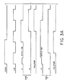
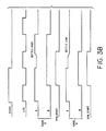
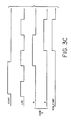
- Figs. 3A-3C Detailed timing diagrams, describing three metastable conditions at both edges of a START signal, are provided in Figs. 3A-3C. These Figures also describe SYN.CONTINUE timing by replacing the START signal with the CONTINUE signal.
- Fig. 3A shows a metastable condition at the leading edge of a START signal.
- Case 1 illustrates flip-flop 12 (see Fig. 2) entering the metastable state and settling to logic "0" within one-half symbol time. In this case, the SYN-START signal is delayed by one and one-half (11 ⁇ 2) symbols.
- Case 2 illustrates a metastable state which settles to a logic "1". In this case, the SYN-START signal is only delayed by one-half (1 ⁇ 2) symbol.
- Fig. 3B shows a falling edge metastable condition. In both Case 3 (flip-flop 12 settles high) and Case 4 (flip-flop 12 settles low), the same SYN-START waveform is generated.
- Fig. 3C shows a timing waveform for the read pointer control logic where a metastable condition does not occur.
- the delay to the SYN-START signal with respect to the START signal in both the Fig. 3B and Fig. 3C cases lies between 1 ⁇ 2 and 11 ⁇ 2 symbols.
- Fig. 4 provides a circuit implementation of an elasticity buffer 10 in accordance with the present invention.
- the read-only INV, J and K registers are hardwired logic "1"s and "0"s, consistent with Table I above.
- the core of the buffer consists of a plurality of nested blocks 22 for any readable and writable bit.
- Fig. 5 The detailed circuitry for a typical nested block 22 is illustrated in Fig. 5, wherein line DI is the data input signal and line DO is the data output signal.
- the XW signal when asserted, allows data to be written in.
- the XR signal when asserted, allows data to be read out.
- Fig. 6 illustrates a design for write pointer control logic which can be used in conjunction with the buffer core shown in Fig. 4.
- a RESET signal clears the first seven D flip-flops and the R-Flag output of the write pointer control logic, but sets the last flip-flop to logic "1".
- the receiver state machine upon receiving a JK start delimiter symbol, the receiver state machine generates a START pulse, generated by the leading edge of SXC, which is clocked into the FXW3 flip-flop at the falling edge of the symbol clock SXC. This asserts the FXW3 signal which, as shown in Fig. 4, writes both the last bit (K1) of the K register and the contents of the A register.
- the receiver state machine when the receiver state machine decodes any repeatable symbols, the REPEAT.DETECT signal is asserted, causing the R-Flag to be asserted as stated above and the cyclic queue is disabled. Since the repeatable symbol is written into the H register setting the R-Flag, the write pointer is cleared at the next clock transition. When a new symbol is detected, the receiver state machine enables the control of the first register in the CONTINUATION section and the cyclic queue configuration is again restored. This design provides a self reset feature which clears all previous shift registers in the write pointer control logic after the assertion of the FXW10 signal.
- a read pointer control circuit which can be used in conjunction with the elasticity buffer 10 is shown in Fig. 7.
- the FXR0 flip-flop is set and all others are cleared. In this state, the read pointer is continuously reading INV symbols.
- the FXR0 signal Upon assertion of either a SYN-START signal or a SYN-CONTINUE signal, the FXR0 signal is de-asserted at the first rising edge of the local clock LXC. If an incoming signal is SYN-START, then the FIFO FXR1 is set at the same rising edge. Thus, the J symbol is read. This read control signal is then shifted sequentially down to the FXR10 flip-flop.
- the read pointer continuously reads the H register until the SYN-CONTINUE signal is issued and it clears the R-Flag. If the R-Flag has not been set, the output of FXR10 flip-flop is fed into the input of FXR5 flip-flop, forming read pointer cyclic queue control. If an incoming signal is SYN-CONTINUE after a reset, the FXR5 flip-flop is set and the START section of the buffer is bypassed. This design also offers a self-reset feature which clears all previous shift registers in the read pointer control logic following the assertion of FXR10.
Landscapes
- Engineering & Computer Science (AREA)
- Computer Networks & Wireless Communication (AREA)
- Signal Processing (AREA)
- Multimedia (AREA)
- Computer Hardware Design (AREA)
- Communication Control (AREA)
- Synchronisation In Digital Transmission Systems (AREA)
- Data Exchanges In Wide-Area Networks (AREA)
- Time-Division Multiplex Systems (AREA)
Applications Claiming Priority (2)
| Application Number | Priority Date | Filing Date | Title |
|---|---|---|---|
| US07/338,587 US5179664A (en) | 1989-04-14 | 1989-04-14 | Symbol-wide elasticity buffer with a read-only section and a read-write section |
| US338587 | 1989-04-14 |
Publications (2)
| Publication Number | Publication Date |
|---|---|
| EP0392397A2 true EP0392397A2 (de) | 1990-10-17 |
| EP0392397A3 EP0392397A3 (de) | 1991-10-30 |
Family
ID=23325356
Family Applications (1)
| Application Number | Title | Priority Date | Filing Date |
|---|---|---|---|
| EP19900106672 Withdrawn EP0392397A3 (de) | 1989-04-14 | 1990-04-06 | Symbolbreite elastische Puffereinrichtung |
Country Status (4)
| Country | Link |
|---|---|
| US (1) | US5179664A (de) |
| EP (1) | EP0392397A3 (de) |
| JP (1) | JPH031739A (de) |
| KR (1) | KR900017328A (de) |
Cited By (1)
| Publication number | Priority date | Publication date | Assignee | Title |
|---|---|---|---|---|
| WO2002054262A3 (en) * | 2001-01-03 | 2003-01-23 | Api Networks Inc | Low latency synchronization of asynchronous data |
Families Citing this family (9)
| Publication number | Priority date | Publication date | Assignee | Title |
|---|---|---|---|---|
| US5842033A (en) * | 1992-06-30 | 1998-11-24 | Discovision Associates | Padding apparatus for passing an arbitrary number of bits through a buffer in a pipeline system |
| US5459731A (en) * | 1993-06-24 | 1995-10-17 | National Semiconductor Corporation | Link error monitoring |
| US5465250A (en) * | 1993-06-24 | 1995-11-07 | National Semiconductor Corporation | Hybrid loopback for FDDI-II slave stations |
| US6597707B1 (en) * | 1999-09-08 | 2003-07-22 | Cypress Semiconductor Corp. | Circuitry, architecture and methods for synchronizing data |
| US6594325B1 (en) | 1999-09-08 | 2003-07-15 | Cypress Semiconductor Corp. | Circuitry, architecture and method(s) for synchronizing data |
| GB2362777B (en) | 2000-05-25 | 2002-05-08 | 3Com Corp | System for detection of asynchronous packet rates and maintenance of maximum theoretical packet rate |
| KR100422141B1 (ko) * | 2000-12-28 | 2004-03-10 | 엘지전자 주식회사 | 정적램을 이용한 링큐 구성 방법 |
| US8131967B2 (en) * | 2007-01-11 | 2012-03-06 | International Business Machines Corporation | Asynchronous data interface |
| US7966435B2 (en) * | 2007-01-11 | 2011-06-21 | International Business Machines Corporation | Integrated circuit design structure for an asychronous data interface |
Family Cites Families (9)
| Publication number | Priority date | Publication date | Assignee | Title |
|---|---|---|---|---|
| US4703486A (en) * | 1984-12-18 | 1987-10-27 | Advanced Micro Devices, Inc. | Communication data encoder/decoder component system architecture |
| US4692894A (en) * | 1984-12-18 | 1987-09-08 | Advanced Micro Devices, Inc. | Overflow/Underflow detection for elastic buffer |
| DE3511430A1 (de) * | 1985-03-29 | 1986-10-02 | Philips Patentverwaltung Gmbh, 2000 Hamburg | Verfahren zur synchronisierung der empfangseinrichtungen in einem digitalen multiplex-uebertragungssystem |
| GB8528890D0 (en) * | 1985-11-23 | 1986-01-02 | Int Computers Ltd | Data transmission system |
| US4945548A (en) * | 1988-04-28 | 1990-07-31 | Digital Equipment Corporation | Method and apparatus for detecting impending overflow and/or underrun of elasticity buffer |
| US4979167A (en) * | 1988-12-02 | 1990-12-18 | Advanced Micro Devices, Inc. | Methods and apparatus for performing restricted token operations on an FDDI network |
| US4984251A (en) * | 1989-08-16 | 1991-01-08 | National Semiconductor Corporation | Method and apparatus for the synchronization of a cascaded multi-channel data transmission |
| US5046182A (en) * | 1989-12-01 | 1991-09-03 | National Semiconductor Corporation | Code points for transferring data from a network transmission medium to a station on the network |
| US5043981A (en) * | 1990-05-29 | 1991-08-27 | Advanced Micro Devices, Inc. | Method of and system for transferring multiple priority queues into multiple logical FIFOs using a single physical FIFO |
-
1989
- 1989-04-14 US US07/338,587 patent/US5179664A/en not_active Expired - Lifetime
-
1990
- 1990-04-06 EP EP19900106672 patent/EP0392397A3/de not_active Withdrawn
- 1990-04-13 KR KR1019900005091A patent/KR900017328A/ko not_active Abandoned
- 1990-04-13 JP JP2096629A patent/JPH031739A/ja active Pending
Cited By (1)
| Publication number | Priority date | Publication date | Assignee | Title |
|---|---|---|---|---|
| WO2002054262A3 (en) * | 2001-01-03 | 2003-01-23 | Api Networks Inc | Low latency synchronization of asynchronous data |
Also Published As
| Publication number | Publication date |
|---|---|
| EP0392397A3 (de) | 1991-10-30 |
| JPH031739A (ja) | 1991-01-08 |
| US5179664A (en) | 1993-01-12 |
| KR900017328A (ko) | 1990-11-16 |
Similar Documents
| Publication | Publication Date | Title |
|---|---|---|
| US4945548A (en) | Method and apparatus for detecting impending overflow and/or underrun of elasticity buffer | |
| JPH055711Y2 (de) | ||
| EP0430051B1 (de) | Bytebreite elastische Puffereinrichtung | |
| US4592072A (en) | Decoder for self-clocking serial data communications | |
| JP3156813B2 (ja) | バッファ制御回路 | |
| EP0339797B1 (de) | Verfahren und Anordnung für Netzwerkknoten zur Vermeidung von Rahmenabstandsschrumpfung | |
| EP0188111A2 (de) | Datenstromsynchronisiereinrichtungen | |
| US5179664A (en) | Symbol-wide elasticity buffer with a read-only section and a read-write section | |
| US5365547A (en) | 1X asynchronous data sampling clock for plus minus topology applications | |
| US6289066B1 (en) | Method and apparatus for recentering an elasticity FIFO when receiving 1000BASE-X traffic using minimal information | |
| EP0393952B1 (de) | Einrichtung und Verfahren zur richtigen Dekodierung in einem Kodierer/Dekodierer | |
| EP0396669B1 (de) | Verfahren und anordnung zur wahrnehmung bevorstehender überläufe und/oder unterschreitungen eines elastischen puffers | |
| US4890304A (en) | Reliable recovery of data in encoder/decoder | |
| US4203003A (en) | Frame search control for digital transmission system | |
| EP0299265A2 (de) | Empfängersynchronisation in einer Anordnung zur Kodierung/Dekodierung | |
| US5903616A (en) | Synchronous clock multiplexer | |
| CA2021348C (en) | Elastic store memory circuit | |
| US4558409A (en) | Digital apparatus for synchronizing a stream of data bits to an internal clock | |
| RU2043652C1 (ru) | Устройство для сопряжения эвм с каналом связи | |
| KR19990004474A (ko) | 패킷 라우터장치 | |
| KR900009356Y1 (ko) | 테이프 레코오더의 재생시 지터 흡수회로 | |
| SU1520530A1 (ru) | Устройство дл сопр жени ЭВМ с каналом св зи | |
| JPH02202733A (ja) | 同期式伝送システムの受信カウンタ位相同期回路 | |
| GB2103053A (en) | Improvements relating to transmission of data in blocks | |
| JPS63139428A (ja) | マンチエスタ符号デコ−ダ回路 |
Legal Events
| Date | Code | Title | Description |
|---|---|---|---|
| PUAI | Public reference made under article 153(3) epc to a published international application that has entered the european phase |
Free format text: ORIGINAL CODE: 0009012 |
|
| AK | Designated contracting states |
Kind code of ref document: A2 Designated state(s): DE FR GB IT NL |
|
| PUAL | Search report despatched |
Free format text: ORIGINAL CODE: 0009013 |
|
| AK | Designated contracting states |
Kind code of ref document: A3 Designated state(s): DE FR GB IT NL |
|
| 17P | Request for examination filed |
Effective date: 19920304 |
|
| 17Q | First examination report despatched |
Effective date: 19931112 |
|
| STAA | Information on the status of an ep patent application or granted ep patent |
Free format text: STATUS: THE APPLICATION IS DEEMED TO BE WITHDRAWN |
|
| 18D | Application deemed to be withdrawn |
Effective date: 19941207 |