EP0388009B1 - Method for forming via holes in polymer materials - Google Patents
Method for forming via holes in polymer materials Download PDFInfo
- Publication number
- EP0388009B1 EP0388009B1 EP90301498A EP90301498A EP0388009B1 EP 0388009 B1 EP0388009 B1 EP 0388009B1 EP 90301498 A EP90301498 A EP 90301498A EP 90301498 A EP90301498 A EP 90301498A EP 0388009 B1 EP0388009 B1 EP 0388009B1
- Authority
- EP
- European Patent Office
- Prior art keywords
- laser beam
- polymer dielectric
- dielectric layer
- predetermined
- scanning
- Prior art date
- Legal status (The legal status is an assumption and is not a legal conclusion. Google has not performed a legal analysis and makes no representation as to the accuracy of the status listed.)
- Expired - Lifetime
Links
Images


Classifications
-
- H—ELECTRICITY
- H05—ELECTRIC TECHNIQUES NOT OTHERWISE PROVIDED FOR
- H05K—PRINTED CIRCUITS; CASINGS OR CONSTRUCTIONAL DETAILS OF ELECTRIC APPARATUS; MANUFACTURE OF ASSEMBLAGES OF ELECTRICAL COMPONENTS
- H05K3/00—Apparatus or processes for manufacturing printed circuits
- H05K3/0011—Working of insulating substrates or insulating layers
- H05K3/0017—Etching of the substrate by chemical or physical means
- H05K3/0026—Etching of the substrate by chemical or physical means by laser ablation
- H05K3/0032—Etching of the substrate by chemical or physical means by laser ablation of organic insulating material
- H05K3/0035—Etching of the substrate by chemical or physical means by laser ablation of organic insulating material of blind holes, i.e. having a metal layer at the bottom
-
- H—ELECTRICITY
- H10—SEMICONDUCTOR DEVICES; ELECTRIC SOLID-STATE DEVICES NOT OTHERWISE PROVIDED FOR
- H10P—GENERIC PROCESSES OR APPARATUS FOR THE MANUFACTURE OR TREATMENT OF DEVICES COVERED BY CLASS H10
- H10P50/00—Etching of wafers, substrates or parts of devices
- H10P50/20—Dry etching; Plasma etching; Reactive-ion etching
- H10P50/28—Dry etching; Plasma etching; Reactive-ion etching of insulating materials
- H10P50/286—Dry etching; Plasma etching; Reactive-ion etching of insulating materials of organic materials
-
- H—ELECTRICITY
- H10—SEMICONDUCTOR DEVICES; ELECTRIC SOLID-STATE DEVICES NOT OTHERWISE PROVIDED FOR
- H10W—GENERIC PACKAGES, INTERCONNECTIONS, CONNECTORS OR OTHER CONSTRUCTIONAL DETAILS OF DEVICES COVERED BY CLASS H10
- H10W20/00—Interconnections in chips, wafers or substrates
- H10W20/01—Manufacture or treatment
- H10W20/071—Manufacture or treatment of dielectric parts thereof
- H10W20/081—Manufacture or treatment of dielectric parts thereof by forming openings in the dielectric parts
- H10W20/082—Manufacture or treatment of dielectric parts thereof by forming openings in the dielectric parts the openings being tapered via holes
-
- H—ELECTRICITY
- H05—ELECTRIC TECHNIQUES NOT OTHERWISE PROVIDED FOR
- H05K—PRINTED CIRCUITS; CASINGS OR CONSTRUCTIONAL DETAILS OF ELECTRIC APPARATUS; MANUFACTURE OF ASSEMBLAGES OF ELECTRICAL COMPONENTS
- H05K2201/00—Indexing scheme relating to printed circuits covered by H05K1/00
- H05K2201/09—Shape and layout
- H05K2201/09818—Shape or layout details not covered by a single group of H05K2201/09009 - H05K2201/09809
- H05K2201/09827—Tapered, e.g. tapered hole, via or groove
-
- H—ELECTRICITY
- H05—ELECTRIC TECHNIQUES NOT OTHERWISE PROVIDED FOR
- H05K—PRINTED CIRCUITS; CASINGS OR CONSTRUCTIONAL DETAILS OF ELECTRIC APPARATUS; MANUFACTURE OF ASSEMBLAGES OF ELECTRICAL COMPONENTS
- H05K2203/00—Indexing scheme relating to apparatus or processes for manufacturing printed circuits covered by H05K3/00
- H05K2203/01—Tools for processing; Objects used during processing
- H05K2203/0147—Carriers and holders
- H05K2203/0165—Holder for holding a Printed Circuit Board [PCB] during processing, e.g. during screen printing
-
- H—ELECTRICITY
- H05—ELECTRIC TECHNIQUES NOT OTHERWISE PROVIDED FOR
- H05K—PRINTED CIRCUITS; CASINGS OR CONSTRUCTIONAL DETAILS OF ELECTRIC APPARATUS; MANUFACTURE OF ASSEMBLAGES OF ELECTRICAL COMPONENTS
- H05K2203/00—Indexing scheme relating to apparatus or processes for manufacturing printed circuits covered by H05K3/00
- H05K2203/02—Details related to mechanical or acoustic processing, e.g. drilling, punching, cutting, using ultrasound
- H05K2203/0207—Partly drilling through substrate until a controlled depth, e.g. with end-point detection
-
- H—ELECTRICITY
- H05—ELECTRIC TECHNIQUES NOT OTHERWISE PROVIDED FOR
- H05K—PRINTED CIRCUITS; CASINGS OR CONSTRUCTIONAL DETAILS OF ELECTRIC APPARATUS; MANUFACTURE OF ASSEMBLAGES OF ELECTRICAL COMPONENTS
- H05K2203/00—Indexing scheme relating to apparatus or processes for manufacturing printed circuits covered by H05K3/00
- H05K2203/09—Treatments involving charged particles
- H05K2203/095—Plasma, e.g. for treating a substrate to improve adhesion with a conductor or for cleaning holes
-
- H—ELECTRICITY
- H05—ELECTRIC TECHNIQUES NOT OTHERWISE PROVIDED FOR
- H05K—PRINTED CIRCUITS; CASINGS OR CONSTRUCTIONAL DETAILS OF ELECTRIC APPARATUS; MANUFACTURE OF ASSEMBLAGES OF ELECTRICAL COMPONENTS
- H05K3/00—Apparatus or processes for manufacturing printed circuits
- H05K3/0008—Apparatus or processes for manufacturing printed circuits for aligning or positioning of tools relative to the circuit board
-
- H—ELECTRICITY
- H05—ELECTRIC TECHNIQUES NOT OTHERWISE PROVIDED FOR
- H05K—PRINTED CIRCUITS; CASINGS OR CONSTRUCTIONAL DETAILS OF ELECTRIC APPARATUS; MANUFACTURE OF ASSEMBLAGES OF ELECTRICAL COMPONENTS
- H05K3/00—Apparatus or processes for manufacturing printed circuits
- H05K3/0011—Working of insulating substrates or insulating layers
- H05K3/0017—Etching of the substrate by chemical or physical means
- H05K3/0041—Etching of the substrate by chemical or physical means by plasma etching
-
- H—ELECTRICITY
- H05—ELECTRIC TECHNIQUES NOT OTHERWISE PROVIDED FOR
- H05K—PRINTED CIRCUITS; CASINGS OR CONSTRUCTIONAL DETAILS OF ELECTRIC APPARATUS; MANUFACTURE OF ASSEMBLAGES OF ELECTRICAL COMPONENTS
- H05K3/00—Apparatus or processes for manufacturing printed circuits
- H05K3/0011—Working of insulating substrates or insulating layers
- H05K3/0055—After-treatment, e.g. cleaning or desmearing of holes
-
- H—ELECTRICITY
- H10—SEMICONDUCTOR DEVICES; ELECTRIC SOLID-STATE DEVICES NOT OTHERWISE PROVIDED FOR
- H10W—GENERIC PACKAGES, INTERCONNECTIONS, CONNECTORS OR OTHER CONSTRUCTIONAL DETAILS OF DEVICES COVERED BY CLASS H10
- H10W70/00—Package substrates; Interposers; Redistribution layers [RDL]
- H10W70/01—Manufacture or treatment
- H10W70/05—Manufacture or treatment of insulating or insulated package substrates, or of interposers, or of redistribution layers
- H10W70/093—Connecting or disconnecting other interconnections thereto or therefrom, e.g. connecting bond wires or bumps
Definitions
- This invention generally relates to a method and apparatus for producing via holes in polymer dielectrics without use of a mask. More particularly, the invention relates to a method for packaging electronic integrated circuit chips disposed on a substrate wherein via openings are produced in a polymer film overlaid on the chips to facilitate electrically interconnecting the chips through the vias thus formed.
- via holes are formed by depositing a metal masking layer over the dielectric layer, patterning the masking layer to expose areas of the dielectric layer where via holes are desired, and then selectively etching the exposed areas of the dielectric layer through the masking layer.
- Either chemical or plasma etching techniques are used to remove the dielectric from the exposed areas, although use of either technique has its own unique drawbacks. Certain dielectric materials cannot conveniently be chemically etched since they absorb chemical etchants, causing damage to the dielectric material underlying the metal masking layer. In addition, some chemical etchants are known to attack metallization, thus requiring special attention when the via being etched is designed to expose an aluminum interconnect pad on a very large scale integrated circuit (VLSI) chip.
- VLSI very large scale integrated circuit
- photo-patternable polymer materials are applied to a substrate and then exposed to light in the areas where via holes are desired. After exposure, the polymer is developed, and baked at high temperatures.
- This method has three prominent limitations. First, it may only be used with photo-patternable materials. Second, the thickness of material which can be photo-patterned is limited to approximately a maximum of 5 microns, due to the inherent properties of the material and sensitizers therefor. Third, the photo-patternable materials must be deposited in liquid form and then merely dried such that they may be easily developed. Prereacted film overlays, such as Kapton® polyimide film available from E.I. du Pont de Nemours and Company, Wilmington, Delaware, cannot be used.
- Another prior method involves forming pillars of conductor material on a substrate and filling in around the pillars with a dielectric.
- a layer of metallization on a substrate is first patterned and the metal is then built up by electroplating to form the pillars.
- Polymer material is then sprayed or spun onto the substrate in multiple coats, leaving sufficient curing time between coats to allow solvent and by-products of the curing process to escape. Enough coats are applied to completely cover the conductors on the substrate, but to barely cover the pillars. Following a short etch sufficient to uncover the top surfaces of the pillars, the pillars can function as metal-filled vias.
- This method has the disadvantages of requiring an excessive number of steps and the use of more difficult wet processing techniques.
- via formation would require at least the steps of damaging the dielectric with the laser, cleaning out the resulting hole with plasma, and thereafter damaging the dielectric at the bottom of the hole with the laser, followed by again cleaning out the hole with plasma.
- Another limitation to this approach is that the surface of the dielectric layer is exposed to excessive amounts of plasma. A substantial amount of plasma is required to clean out the holes and the undamaged dielectric surface tends to become rough from exposure to the plasma. The rough surface makes subsequent metallizations difficult to pattern.
- Pulsed lasers such as excimer and doubled YAG lasers have been used to directly ablate dielectric layers.
- laser energy is absorbed in a thin layer of the dielectric in sufficient amounts to evaporate or ablate the thin layer of dielectric where the laser beam impinges.
- Multiple pulses are required to ablate holes of increased depth. Care must be taken to avoid ablating the underlying metal with laser pulses since the energy necessary to heat the polymer to ablation temperatures can also destroy the metallization underlying the dielectric.
- To effectively practice this method only very small thicknesses of dielectric may be removed per pulse and, as a result, the method requires an excessive number of pulses. Lasers emitting visible light are not acceptable for this ablation technique because the penetration depth is too great.
- the direct laser ablation technique limits electronic package manufacturers to use of circular via holes. Round vias, however, are not as good as rectangular vias since they limit the area available for electrical contact; that is, rectangular vias are easily enlarged into larger rectangular vias without leaving residual materials in the bottom of the holes. Yet.the shape of the via holes formed using this technique is unavoidably circular because the laser energy is a focussed version of the laser cavity. Even if a non-circular mask opening is used as an aperture, the laser lens will nevertheless focus the energy as a circle. Changing via hole sizes requires a sophisticated zoom lens which can change focal length and f number to balance the conflicting optical requirements for hole size variation and constant depth of focus.
- Direct laser ablation techniques also do not allow for creation of sufficiently narrow via hole sizes in thick dielectrics, i.e., dielectrics too thick to be patterned by conventional photoresist techniques.
- the top of the hole is necessarily larger for larger thicknesses of dielectric, with the result that hole size at the top becomes too large when working with thick dielectrics.
- thick dielectrics are desirable for many applications. When working with self-standing dielectric films, thicker films are easier to handle. Thick dielectrics are advantageous in systems where capacitance of conductor lines must be minimized.
- thick dielectrics are preferred for compliance with radiation hardness requirements - the dielectric must be sufficiently thick to absorb the secondary electrons generated by conductors overlying semiconductors.
- GB-A-1583193 discloses a method of manufacturing a flexible printed circuit board which includes the operations of depositing a layer of copper upon a base flexible insulating layer made of polyester, photo-etching the copper layer by means of techniques which are well-known in the art of manufacturing electronic devices to provide a system of conductors, and over-layer the system of conductors with a second flexible insulating layer.
- a second reflecting, copper layer is then deposited on the flexible insulating layer and photo-etched using the same techniques as before, to provide holes which coincide with those regions of the conductors which it is desired to expose to enable separate components of the electrical circuit to be soldered to the conductors to form the desired electrical circuit. Other holes are formed in the second copper layer to delineate the final flexible printed circuit.
- the assembly is then subjected to a laser machining operation in which a focused laser beam is scanned over the surface of the second copper layer.
- the laser beam vapourises the insulating layer where is it exposed by the holes in the second copper layer, thus clearing the desired regions of conductors and cutting out the printed circuit.
- the second copper layer is then removed before the separate components are soldered into place.
- the second copper layer can be removed by any convenient process.
- a carbon dioxide gas laser having a power output of about 400 watts is suitable for carrying out the process.
- the method which may be performed under direct computer control without use of masks and without causing damage to the underlying conductor material, may be used for forming via holes in thick dielectrics in a stepped profile for minimum hole sizes and maximum hole densities.
- a method for producing via holes in a polymer dielectric layer comprising the steps of scanning without masking a first predetermined area of the polymer dielectric layer with a laser beam in a predetermined pattern at a sufficient level of energy and speed to heat a small volume of the polymer dielectric to a point of vaporization during a predetermined laser beam dwell time, said volume being the product of the laser beam maximum energy spot area and the depth of a surface layer portion of the polymer dielectric layer; and repeating said scanning of said area for a sufficient number of times to etch a first desired amount of polymer dielectric layer from said predetermined area.
- a continuous wave laser beam is focused to a very high energy density and dithered or scanned at a high scan rate, while also being advanced in a direction perpendicular to the dither direction so as to move over the entire area to a dielectric where a via hole is to be formed.
- the energy density in the focused spot must be sufficient to heat a surface layer of the dielectric material within that spot to the point of vaporization or dissociation of the polymer. This constitutes what is known as ablation.
- the duty cycle must be such that the surrounding dielectric material is not heated to a degree which causes damage, and the wavelength of the laser must be such that a predominant portion of the energy is absorbed in a very thin uppermost section of the dielectric.
- the hole may be scanned in a raster format, which allows complete control over the size and shape of the hole.
- the laser removes a small amount of dielectric material on each scan and the scans are repeated until the underlying metallization is exposed.
- the output of the laser, the scanning or dithering (i.e., rapid to-and-fro movement) of the laser beam, and movement of an X-Y table carrying the structure undergoing ablation, may be controlled by computer.
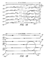
- Figures 1A and 1B are top view illustrations of two alternative scan patterns which may be used to produce a typical via hole.
- Figure 1A illustrates a raster scan pattern for application to a surface onto which a focussed laser beam spot 120 impinges.
- the parallel scans of the laser beam are all in the same direction, each being 25 microns in extent.
- the solid lines 100, 102, 104, 106, 108, 110 and 112 indicate the paths along which the laser beam is scanned, in sequence, in the direction of the arrows.
- Each of these paths may be considered to be in an easterly direction (or +X direction in a Cartesian coordinate system). After each easterly scan, there is a relatively brief time delay before the next scan.
- the laser beam is blocked, or turned off, while it is repositioned relative to the area being scanned (as though the beam were moved generally westerly along the diagonal, dashed lines 101, 103, 105, 107, 109 and 111, in sequence).
- path 101 is traversed after scan 100, and is followed by scan 102, then path 103, etc.
- the incrementation in the southerly (or -Y) direction is such that parallel scan lines 100, 102, 104, 106, 108, 110 and 112 are spaced 1 micron apart. Scanning is done at the rate of three meters per second.
- the diameter of the maximum energy spot 120 is approximately 3 microns.
- Figure 1B shows an alternative scan pattern which may be considered as a modified raster scan.
- This scan pattern differs from that shown in Figure 1A in that the laser beam is scanned in both X directions.
- the laser beam scans along lines 130, 134, 138, and 142 by moving easterly (in the +X direction), while in alternate scans along lines 132, 136 and 140 the beam moves westerly (in the -X direction).
- the laser beam is turned off, or blocked, while it is incremented between successive east-west scans (as though it were moved southerly along each of the dashed lines 131, 133, 135, 137, 139 and 141) by 1 micron. Spacing between adjacent scan lines is thus 1 micron.
- the maximum energy spot 150 is approximately 3 microns in diameter.
- the etching process for the scan pattern of Figure 1A is thus similar to that for the scan pattern of Figure 1B, while those skilled in the art will recognize that other scan patterns can be devised to effect the same etching process.
- a dielectric polymeric layer of Kapton polyimide or of silicone-polyimide can be etched in approximately 4 raster scans. Since the maximum energy spot size is approximately 3 microns in diameter, the spot overlaps the scan lines, which are spaced apart from each other by 1 micron, by a factor of 3. Thus in 4 raster scans, the same area is scanned by the laser beam a total of 12 times (i.e., 3 overlaps multiplied by 4 scans). A depth of approximately 2.5 microns of dielectric material is removed by each scan of the laser beam, so that approximately 30 microns of material is removed during the 12 passes made by the laser beam.
- the power density of the spot is 3.3x10⁶ watts per square centimeter (watt/cm2).
- the surface layer, or depth of dielectric material to which the laser energy penetrates before being virtually completely absorbed is 1-3 microns, depending on the material.
- the approximate volume of material exposed to the laser beam is the product of the maximum energy spot size area and the absorption depth (where dwell time may be defined as the time for which any given point is exposed to the energy of the maximum energy spot area of the passing beam).
- This extremely small volume can be heated to vaporization temperature in less than 1 microsecond by the 3.3x10⁶ watt/cm2 energy density spot.
- the system works effectively because very small volumes of material are vaporized at very fast rates, much like machining away a small amount of material in a conventional machining operation.
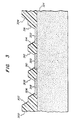
- FIGS 2A through 2C illustrate progression of the via hole formation process of the invention from 1 raster scan to the next.
- a continuous wave laser beam 200 is focused to a very high energy density over a dielectric polymer layer 202, which is situated atop a metal contact pad 204 on a substrate 206.
- Substrate 206 may comprise an integrated circuit chip, in which case contact pad 204 comprises a chip pad thereon.
- substrate 206 may comprise a multilevel printed circuit board or ceramic multilayer substrate for hybrid assemblies in which case layer 204 is a metal run and layer 206 is insulation between successive, vertically-stacked metal runs.
- metal run 204 may be situated directly on a printed circuit board 206.
- Figures 2A and 2B show the effect of laser beam 200 being scanned across polymer layer 202. Beam scanning occurs at a rate of 3 meters per second. As shown in Figure 2C, laser beam 200 is reflected when the beam reaches metal contact pad 204. Since well over half the energy of the beam is reflected by pad 204 and since pad 204 is highly thermally conductive and exhibits a substantially higher thermal diffusivity than the material of polymer layer 202, the surface temperature of pad 204 remains well below the metal vaporization point. As a result, the drilling action ceases when the metal pad has been exposed.
- the laser beam impinges on polymer layer 202 only 1% of the time, such that only 1% of the laser power, or 2.5 milliwatts, is applied to the via during its formation. This amount of power is well below the threshold for damage to adjacent areas of polymer 202.
- the sides of the hole formed by this laser drilling action such as sides 210 and 212, slope toward the center because they do not experience the overlapping scans that occur in the central portions of the hole and the etching process therefore proceeds more slowly at the sides of the hole. If the raster is scanned more times than required to reach underlying metal pad 204, sides 210 and 212 of the hole will be steepened somewhat from their illustrated slopes.
- the via holes produced by the laser beam are cleaned by a short plasma etch cycle which removes from underlying metal pad 240 any particles formed during the laser beam scanning,such as soot, any residual polymer, or any glass that may be residual from any glass removal operation performed when etching a pad mask, and cleans and roughens the upper surface of dielectric polymer layer 202 in order to enhance adhesion of subsequent metallization.
- the presently preferred plasma etch technique is to preheat both the part (i.e., substrate) and chamber in which the part is placed, to a temperature of 110°C, and then to etch the part for 2 minutes at a power of 150 watts in an atmosphere of 20% CF4 and 80% 02. This assumes that four 50,8x50,8 mm (2''x2'') substrates are etched in the chamber.
- the amount of polymer dielectric etched by this technique is between 2 and 4 microns.
- Figure 3 illustrates an application of the method of the present invention to increase the number of via holes possible in a given area in thick dielectric polymer layers.
- the dielectric polymer layer 300 has first been scanned by the laser beam across a relatively large area to produce the opening that extends from side 302 to side 304, but with only a sufficient number of scans to remove a portion of the depth of the polymer material. This is the result of large scans or dithers between side 302 and side 304, which cause ablation to a depth, in this case, of approximately one-half the thickness of polymer layer 300.
- each of the three via holes is still relatively small in diameter at its respective top.
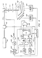
- FIG 4 illustrates laser apparatus for forming via holes by the laser beam dither method of the present invention.
- Laser 410 may be a 3.5 watt Spectra Physics 2035-35 argon ion laser with ultraviolet optics. This is a continuous wave (CW) laser which emits ultraviolet radiation. The main ultraviolet line is 351 nanometers, and the laser power output is nominally 1.2 watts.
- the beam produced by the laser is modulated by a modulator, such as an acousto-optical modulator 412.
- a modulator such as an acousto-optical modulator 412.
- One such acousto-optical modulator useable in the invention is a Newport Electro Optics Quartz 35080-3 modulator.
- the modulated laser beam 414 strikes a scanning mirror 416 and is reflected to a lens 418 which focuses it upon a substrate 420 situated an an XY positioning table 422 which allows movement of the chip in an X or Y direction relative to the laser beam.
- Substrate 420 may comprise a dielectric polymer layer overlying an integrated circuit chip. It will be appreciated by those skilled in the art that, in the alternative, other laser beam deflectors such as rotating mirrors, acousto optic deflection devices, or similar devices designed to deflect light in a precise manner, could be substituted for scanning mirror 416.
- the XY positioning table may be a Klinger Scientific model TCS 250-200 table.
- Lens 418 focuses what is preferably a 3 millimeter diameter laser beam 414 to a spot 424 having a maximum energy region diameter of 3 microns. This lens is selected to keep the laser beam continually in focus on the area of dielectric polymer layer that is to be ablated.
- lens 418 may comprise a field-flattening lens capable of focusing ultraviolet energy.
- the laser beam is scanned in the east/west (i.e., ⁇ X) direction preferably by a General Scanning G120D galvanometer 415 which sweeps scanning mirror 416 in response to a ramp voltage output from amplifier 426.
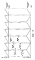
- the ramp voltage appears as one or the other waveforms depicted in Figure 5.
- the laser beam is scanned in easterly directions only, and the waveform appears as designated for easterly scans; i.e., a relatively slowly rising ramp voltage followed by a relatively rapid flyback or return to the starting voltage level, designated O, and a repetition of the rising ramp voltage, etc.
- the laser beam is on for either the full extent of the rise or some predetermined portion thereof, and during the falling voltage the beam is off.
- the laser beam is dithered, or alternately scanned in an easterly direction and a westerly direction, and the waveform appears as designated for east/west scans; i.e., a rising ramp voltage (easterly scan) followed by a brief pause at the maximum voltage, and thereafter a falling ramp voltage (westerly scan) followed by a brief pause at the starting voltage level, designated O, and a repetition of the rising ramp voltage, etc.
- an AND gate 428 having one input energized by a controller 430 controls modulator 412 to either pass or block the laser beam.
- Controller 430 which may comprise a programmed IBM Personal Computer (PC), also controls positioning of XY table 422 through servo motor controls 432 for the north/south (i.e., ⁇ Y) direction and 434 for the east/west direction.
- PC IBM Personal Computer
- Controller 430 loads ON and OFF values in latches or registers 436 and 438 which define the extent or limits of the east/west laser beam scanning introduced by galvanometer-controlled scanning mirror 416.
- Each respective one of latches 436 and 438 may comprise a Texas Instruments 74LS374 latch.
- Counter logic 440 operates under the control of controller 430 to provide an output count to ON and OFF comparators 442 and 444, respectively, each of which may comprise a Texas Instruments 74521 8-bit comparator, respectively.
- comparator 442 produces an ON output signal which sets a flip-flop 446.
- comparator 444 when the count from counter logic 440 equals the value stored in latch 438, comparator 444 produces an OFF output signal which resets flip-flop 446.
- Comparators 442 and 444, together with flip-flop 446, comprise switching circuitry 450.
- the Q or true output of flip-flop 446 supplies an input voltage to AND gate 428, while the Q or false output of flip-flop 446 supplies an input voltage to both counter logic 440 and controller 430.
- the count output from counter logic 440 is also supplied to a digital-to-analog converter 448, such as an Analog Devices AD656 converter, which generates the scanning ramp voltage that is supplied to amplifier 426.
- the output signal produced by AND gate 428 defines the time during which the laser beam is passed by modulator 412, and this in turn corresponds to the duration of the easterly or westerly scan of the laser beam on the substrate by galvanometer-controlled scanning mirror 416.
- the XY table 422 is commanded by controller 430 to the appropriate position for beginning the etching process. This is accomplished in a manner well known in the art by actuating motor controls 432 and 434 to cause table 422 to rapidly arrive at the beginning scan position.
- controller 430 loads latches 436 and 438 with the appropriate ON and OFF values for the area to be etched. As will be understood by those skilled in the art, the values loaded in latches 436 and 438 may be selected to control both length and position of the laser beam scans, depending on the specific implementation of the invention.
- controller 430 enables AND gate 428 in the manner previously mentioned, and the first easterly scan of the laser beam commences.
- controller 430 moves the XY table in the southerly direction by 1 micron and initiates either another easterly scan of the beam, for the raster scan pattern of Figure 1A, or a westerly scan of the beam, for the raster scan pattern of Figure IB, by driving galvanometer-controlled scanning mirror 416 in the appropriate direction.
- the process is repeated with the XY table being incremented in the southerly direction by step pulses from controller 430 for each scan of the laser beam resulting from motion of mirror 416.
- the next raster is scanned with the XY table being incremented in the northerly direction for each scan of the laser beam resulting from motion of mirror 416.
- controller 430 deenergizes its input to AND gate 428 to shut off the laser beam, and appropriately energizes motor controls 432 and 434 to move the XY table to the next location where a via hole is desired.
- Hole size in the east/west direction is controlled by the numbers loaded into latches 436 and 438.
- Hole size in the north/south direction is controlled by the number of step pulses supplied from controller 430 to Y axis motor control 432.
- Y axis control 432 thus serves a dual purpose: first, acting as a slew servo to rapidly position XY table 422 in cooperation with X axis control 434, and second, acting as an incrementing servo to control the extent of the raster scan in the north/south or ⁇ Y direction. Controller 430 controls both of these modes of operation of Y axis control 432.
- counter logic 430 is shown in detail in Figure 6. This implementation produces the raster scan shown in Figure 1A.
- the logic comprises a counter 510, such as a Texas Instruments 74163 counter, which is initially reset by controller 430 via OR gate 514 and counts in response to clock pulses supplied via AND gate 512 when enabled by controller 430.
- the count output of counter 510 is supplied to ON and OFF comparators 442 and 444 and D/A converter 448, shown in Figure 4.
- a reset signal is supplied to AND gate 516 which is enabled by the Q output voltage from flip-flop 446.
- the values loaded in latches 436 and 438 of Figure 4 do not represent the full extent of the east/west scan of the laser beam produced by mirror 416, but only that portion of the scan during which the laser beam is passed by modulator 412.
- the scan i.e., motion of mirror 416
- the laser beam can be made to scan through only the most linear portion of each sweep of galvanometer 415 to achieve uniform ablation over the scanning area of the dielectric polymer layer.
- the beam may thus be controlled to pass through only the most central portion of lens 418 to ensure that beam distortion introduced by the lens is minimized.
- the XY table is incremented in the southerly direction during the flyback portion of the voltage waveform shown in Figure 1A.
- the entire process is somewhat analogous to television raster scanning, a major exception being that incremental movement takes place in either direction on the Y axis, depending on the "frame" being scanned.
- counter 510 is an up/down counter and the decoding logic 518 detects both a predetermined count and a zero count. The result of either detected count does not reset counter 510 but rather controls the direction of counting of the counter. Accordingly, in the presence of a signal from controller 430, clock pulses supplied through AND gate 512 drive counter 510 to continuously count up and down between a zero count and a predetermined count, and the count output of counter 510 is supplied to comparators 442 and 444 and to D/A converter 448.
- the voltage waveform output from D/A converter 448 is now generally a triangular wave, as indicated for the east/west scans in Figure 5, rather than a sawtooth wave as indicated for the easterly scans in Figure 5; that is, the signal controlling galvanometer mirror 416 ramps in two directions rather than just one.
- PC controller 430 must supply data to the on and off latches 436 and 438 to coincide with each east or west direction of scan.
Landscapes
- Engineering & Computer Science (AREA)
- Physics & Mathematics (AREA)
- Optics & Photonics (AREA)
- Manufacturing & Machinery (AREA)
- Microelectronics & Electronic Packaging (AREA)
- Laser Beam Processing (AREA)
- Drying Of Semiconductors (AREA)
- Internal Circuitry In Semiconductor Integrated Circuit Devices (AREA)
- Lasers (AREA)
Description
- This invention generally relates to a method and apparatus for producing via holes in polymer dielectrics without use of a mask. More particularly, the invention relates to a method for packaging electronic integrated circuit chips disposed on a substrate wherein via openings are produced in a polymer film overlaid on the chips to facilitate electrically interconnecting the chips through the vias thus formed.
- Formation of via holes to allow for electrical connection between two or more layers of conductor separated by a layer of dielectric material has heretofore been accomplished by several methods, each of which has limitations.
- In one prior method, via holes are formed by depositing a metal masking layer over the dielectric layer, patterning the masking layer to expose areas of the dielectric layer where via holes are desired, and then selectively etching the exposed areas of the dielectric layer through the masking layer. Either chemical or plasma etching techniques are used to remove the dielectric from the exposed areas, although use of either technique has its own unique drawbacks. Certain dielectric materials cannot conveniently be chemically etched since they absorb chemical etchants, causing damage to the dielectric material underlying the metal masking layer. In addition, some chemical etchants are known to attack metallization, thus requiring special attention when the via being etched is designed to expose an aluminum interconnect pad on a very large scale integrated circuit (VLSI) chip. The anisotropic nature of plasma etching tends to produce barrel-shaped via holes. Depositing metallization in barrel-shaped via holes is very difficult. Moreover, thickness variations in the dielectric layer being etched may result in excessive plasma etching in certain areas with marginal etching in others.
- In another known method, photo-patternable polymer materials are applied to a substrate and then exposed to light in the areas where via holes are desired. After exposure, the polymer is developed, and baked at high temperatures. This method has three prominent limitations. First, it may only be used with photo-patternable materials. Second, the thickness of material which can be photo-patterned is limited to approximately a maximum of 5 microns, due to the inherent properties of the material and sensitizers therefor. Third, the photo-patternable materials must be deposited in liquid form and then merely dried such that they may be easily developed. Prereacted film overlays, such as Kapton® polyimide film available from E.I. du Pont de Nemours and Company, Wilmington, Delaware, cannot be used.
- Another prior method involves forming pillars of conductor material on a substrate and filling in around the pillars with a dielectric. In this method, a layer of metallization on a substrate is first patterned and the metal is then built up by electroplating to form the pillars. Polymer material is then sprayed or spun onto the substrate in multiple coats, leaving sufficient curing time between coats to allow solvent and by-products of the curing process to escape. Enough coats are applied to completely cover the conductors on the substrate, but to barely cover the pillars. Following a short etch sufficient to uncover the top surfaces of the pillars, the pillars can function as metal-filled vias. This method has the disadvantages of requiring an excessive number of steps and the use of more difficult wet processing techniques.
- Eichelberger et al. U.S. Patent 4,714,516, issued December 22, 1987 and assigned to the present applicants discloses the use of an argon ion laser to form vias. Selected areas of the dielectric are damaged with laser energy and the damaged areas are then etched with oxygen plasma. The damaged portion of the dielectric etches at a much higher rate than the undamaged portion. One qualification on use of this approach arises because hole depth is limited by the amount of damage at the surface; that is, the via hole must be at least as wide at the top as the thickness of the dielectric material to be drilled. As a practical matter, via hole depths are limited to about 10 microns; therefore, thicker dielectric material requires extra steps in the formation of a via. For example, via formation would require at least the steps of damaging the dielectric with the laser, cleaning out the resulting hole with plasma, and thereafter damaging the dielectric at the bottom of the hole with the laser, followed by again cleaning out the hole with plasma. Another limitation to this approach is that the surface of the dielectric layer is exposed to excessive amounts of plasma. A substantial amount of plasma is required to clean out the holes and the undamaged dielectric surface tends to become rough from exposure to the plasma. The rough surface makes subsequent metallizations difficult to pattern.
- Pulsed lasers such as excimer and doubled YAG lasers have been used to directly ablate dielectric layers. By this technique, laser energy is absorbed in a thin layer of the dielectric in sufficient amounts to evaporate or ablate the thin layer of dielectric where the laser beam impinges. Multiple pulses are required to ablate holes of increased depth. Care must be taken to avoid ablating the underlying metal with laser pulses since the energy necessary to heat the polymer to ablation temperatures can also destroy the metallization underlying the dielectric. To effectively practice this method, only very small thicknesses of dielectric may be removed per pulse and, as a result, the method requires an excessive number of pulses. Lasers emitting visible light are not acceptable for this ablation technique because the penetration depth is too great.
- The direct laser ablation technique limits electronic package manufacturers to use of circular via holes. Round vias, however, are not as good as rectangular vias since they limit the area available for electrical contact; that is, rectangular vias are easily enlarged into larger rectangular vias without leaving residual materials in the bottom of the holes. Yet.the shape of the via holes formed using this technique is unavoidably circular because the laser energy is a focussed version of the laser cavity. Even if a non-circular mask opening is used as an aperture, the laser lens will nevertheless focus the energy as a circle. Changing via hole sizes requires a sophisticated zoom lens which can change focal length and f number to balance the conflicting optical requirements for hole size variation and constant depth of focus.
- Direct laser ablation techniques also do not allow for creation of sufficiently narrow via hole sizes in thick dielectrics, i.e., dielectrics too thick to be patterned by conventional photoresist techniques. The top of the hole is necessarily larger for larger thicknesses of dielectric, with the result that hole size at the top becomes too large when working with thick dielectrics. Yet thick dielectrics are desirable for many applications. When working with self-standing dielectric films, thicker films are easier to handle. Thick dielectrics are advantageous in systems where capacitance of conductor lines must be minimized. In addition, thick dielectrics are preferred for compliance with radiation hardness requirements - the dielectric must be sufficiently thick to absorb the secondary electrons generated by conductors overlying semiconductors.
- GB-A-1583193 discloses a method of manufacturing a flexible printed circuit board which includes the operations of depositing a layer of copper upon a base flexible insulating layer made of polyester, photo-etching the copper layer by means of techniques which are well-known in the art of manufacturing electronic devices to provide a system of conductors, and over-layer the system of conductors with a second flexible insulating layer. A second reflecting, copper layer is then deposited on the flexible insulating layer and photo-etched using the same techniques as before, to provide holes which coincide with those regions of the conductors which it is desired to expose to enable separate components of the electrical circuit to be soldered to the conductors to form the desired electrical circuit. Other holes are formed in the second copper layer to delineate the final flexible printed circuit. The assembly is then subjected to a laser machining operation in which a focused laser beam is scanned over the surface of the second copper layer. The laser beam vapourises the insulating layer where is it exposed by the holes in the second copper layer, thus clearing the desired regions of conductors and cutting out the printed circuit. The second copper layer is then removed before the separate components are soldered into place. The second copper layer can be removed by any convenient process.
- A carbon dioxide gas laser having a power output of about 400 watts is suitable for carrying out the process.
- It is an object of this invention to provide a method for forming via holes of various sizes and shapes in dielectrics of various types and thicknesses, including fully-reacted films, at commercial rates and with a minimum number of processing steps. The method, which may be performed under direct computer control without use of masks and without causing damage to the underlying conductor material, may be used for forming via holes in thick dielectrics in a stepped profile for minimum hole sizes and maximum hole densities.
- According to the present invention, there is provided a method for producing via holes in a polymer dielectric layer comprising the steps of scanning without masking a first predetermined area of the polymer dielectric layer with a laser beam in a predetermined pattern at a sufficient level of energy and speed to heat a small volume of the polymer dielectric to a point of vaporization during a predetermined laser beam dwell time, said volume being the product of the laser beam maximum energy spot area and the depth of a surface layer portion of the polymer dielectric layer; and repeating said scanning of said area for a sufficient number of times to etch a first desired amount of polymer dielectric layer from said predetermined area.
- Briefly, in accordance with a preferred embodiment of the invention, a continuous wave laser beam is focused to a very high energy density and dithered or scanned at a high scan rate, while also being advanced in a direction perpendicular to the dither direction so as to move over the entire area to a dielectric where a via hole is to be formed. The energy density in the focused spot must be sufficient to heat a surface layer of the dielectric material within that spot to the point of vaporization or dissociation of the polymer. This constitutes what is known as ablation. The duty cycle must be such that the surrounding dielectric material is not heated to a degree which causes damage, and the wavelength of the laser must be such that a predominant portion of the energy is absorbed in a very thin uppermost section of the dielectric. The hole may be scanned in a raster format, which allows complete control over the size and shape of the hole. During this process, the laser removes a small amount of dielectric material on each scan and the scans are repeated until the underlying metallization is exposed. The output of the laser, the scanning or dithering (i.e., rapid to-and-fro movement) of the laser beam, and movement of an X-Y table carrying the structure undergoing ablation, may be controlled by computer.
- The objectives and advantages of the invention in various aspects thereof will be better understood from the following detailed description of a preferred embodiment of the invention with reference to the drawings, in which:
- Figures 1A and 1B are plan views of alternative laser beam scan patterns which may be used for etching a via hole;
- Figures 2A, 2B and 2C are progressive cross-sectional side views illustrating the results of laser beam dithering carried out in accordance with the present invention;
- Figure 3 is a cross-sectional side view of a group of closely spaced via holes with sloping sidewalls formed in a two-step process employing the laser beam dithering of the present invention;
- Figure 4 is a part block and part schematic diagram of laser apparatus for carrying out the method of the present invention;
- Figure 5 illustrates ramp voltage waveforms generated in the circuit of Figure 4 to produce the laser beam scan patterns shown in Figures 1A and 1B; and
- Figure 6 is a block diagram of one example of counter logic circuitry for use in the apparatus shown in Figure 4.
- Figures 1A and 1B are top view illustrations of two alternative scan patterns which may be used to produce a typical via hole. Figure 1A illustrates a raster scan pattern for application to a surface onto which a focussed
laser beam spot 120 impinges. The parallel scans of the laser beam are all in the same direction, each being 25 microns in extent. Thesolid lines lines path 101 is traversed afterscan 100, and is followed byscan 102, thenpath 103, etc. The incrementation in the southerly (or -Y) direction is such thatparallel scan lines maximum energy spot 120 is approximately 3 microns. After traversal of a raster has been completed, the process is repeated with the easterly scans progressing in the northerly (or+Y) direction relative to the area being scanned. - Figure 1B shows an alternative scan pattern which may be considered as a modified raster scan. This scan pattern differs from that shown in Figure 1A in that the laser beam is scanned in both X directions. Thus, the laser beam scans along
lines lines lines maximum energy spot 150 is approximately 3 microns in diameter. The etching process for the scan pattern of Figure 1A is thus similar to that for the scan pattern of Figure 1B, while those skilled in the art will recognize that other scan patterns can be devised to effect the same etching process. - As a specific example of the etching process according to the invention, a dielectric polymeric layer of Kapton polyimide or of silicone-polyimide, 25 to 30 microns in thickness, can be etched in approximately 4 raster scans. Since the maximum energy spot size is approximately 3 microns in diameter, the spot overlaps the scan lines, which are spaced apart from each other by 1 micron, by a factor of 3. Thus in 4 raster scans, the same area is scanned by the laser beam a total of 12 times (i.e., 3 overlaps multiplied by 4 scans). A depth of approximately 2.5 microns of dielectric material is removed by each scan of the laser beam, so that approximately 30 microns of material is removed during the 12 passes made by the laser beam. Since the beam is focussed to a spot of maximum energy in a diameter of 3 microns and the power within that spot is 0.25 watts, then the power density of the spot is 3.3x10⁶ watts per square centimeter (watt/cm²). At a laser wavelength of 351 nanometers, the surface layer, or depth of dielectric material to which the laser energy penetrates before being virtually completely absorbed, is 1-3 microns, depending on the material. For a laser beam dwell time of 1 microsecond, the approximate volume of material exposed to the laser beam is the product of the maximum energy spot size area and the absorption depth (where dwell time may be defined as the time for which any given point is exposed to the energy of the maximum energy spot area of the passing beam). This is a 3 micron depth multiplied by the roughly square (but with rounded corners) area exposed to a 3 micron diameter spot, or approximately 2.7x10⁻¹¹ cm³. This extremely small volume can be heated to vaporization temperature in less than 1 microsecond by the 3.3x10⁶ watt/cm² energy density spot. The system works effectively because very small volumes of material are vaporized at very fast rates, much like machining away a small amount of material in a conventional machining operation.
- Figures 2A through 2C illustrate progression of the via hole formation process of the invention from 1 raster scan to the next. A continuous
wave laser beam 200 is focused to a very high energy density over adielectric polymer layer 202, which is situated atop ametal contact pad 204 on asubstrate 206.Substrate 206 may comprise an integrated circuit chip, in whichcase contact pad 204 comprises a chip pad thereon. Alternatively,substrate 206 may comprise a multilevel printed circuit board or ceramic multilayer substrate for hybrid assemblies in whichcase layer 204 is a metal run andlayer 206 is insulation between successive, vertically-stacked metal runs. As another alternative,metal run 204 may be situated directly on a printedcircuit board 206. Figures 2A and 2B show the effect oflaser beam 200 being scanned acrosspolymer layer 202. Beam scanning occurs at a rate of 3 meters per second. As shown in Figure 2C,laser beam 200 is reflected when the beam reachesmetal contact pad 204. Since well over half the energy of the beam is reflected bypad 204 and sincepad 204 is highly thermally conductive and exhibits a substantially higher thermal diffusivity than the material ofpolymer layer 202, the surface temperature ofpad 204 remains well below the metal vaporization point. As a result, the drilling action ceases when the metal pad has been exposed. In the present embodiment, the laser beam impinges onpolymer layer 202 only 1% of the time, such that only 1% of the laser power, or 2.5 milliwatts, is applied to the via during its formation. This amount of power is well below the threshold for damage to adjacent areas ofpolymer 202. The sides of the hole formed by this laser drilling action, such assides underlying metal pad 204,sides - The via holes produced by the laser beam are cleaned by a short plasma etch cycle which removes from underlying metal pad 240 any particles formed during the laser beam scanning,such as soot, any residual polymer, or any glass that may be residual from any glass removal operation performed when etching a pad mask, and cleans and roughens the upper surface of
dielectric polymer layer 202 in order to enhance adhesion of subsequent metallization. The presently preferred plasma etch technique is to preheat both the part (i.e., substrate) and chamber in which the part is placed, to a temperature of 110°C, and then to etch the part for 2 minutes at a power of 150 watts in an atmosphere of 20% CF₄ and 80% 0₂. This assumes that four 50,8x50,8 mm (2''x2'') substrates are etched in the chamber. The amount of polymer dielectric etched by this technique is between 2 and 4 microns. - Figure 3 illustrates an application of the method of the present invention to increase the number of via holes possible in a given area in thick dielectric polymer layers. The
dielectric polymer layer 300, as shown, has first been scanned by the laser beam across a relatively large area to produce the opening that extends fromside 302 toside 304, but with only a sufficient number of scans to remove a portion of the depth of the polymer material. This is the result of large scans or dithers betweenside 302 andside 304, which cause ablation to a depth, in this case, of approximately one-half the thickness ofpolymer layer 300. Then the three smaller openings betweenside 306 andside 308, betweenside 310 andside 312, and betweenside 314 andside 316, respectively, are formed using two additional raster scans of reduced dimensions. These three smaller openings extend all the way down tometal pads substrate 324, so as to constitute vias having sloping sidewalls to facilitate metallization. Despite the relative depth of these three via holes and the relative thickness ofpolymer layer 300, each of the three via holes is still relatively small in diameter at its respective top. - Figure 4 illustrates laser apparatus for forming via holes by the laser beam dither method of the present invention.
Laser 410 may be a 3.5 watt Spectra Physics 2035-35 argon ion laser with ultraviolet optics. This is a continuous wave (CW) laser which emits ultraviolet radiation. The main ultraviolet line is 351 nanometers, and the laser power output is nominally 1.2 watts. The beam produced by the laser is modulated by a modulator, such as an acousto-optical modulator 412. One such acousto-optical modulator useable in the invention is a Newport Electro Optics Quartz 35080-3 modulator. The modulatedlaser beam 414 strikes ascanning mirror 416 and is reflected to alens 418 which focuses it upon asubstrate 420 situated an an XY positioning table 422 which allows movement of the chip in an X or Y direction relative to the laser beam.Substrate 420 may comprise a dielectric polymer layer overlying an integrated circuit chip. It will be appreciated by those skilled in the art that, in the alternative, other laser beam deflectors such as rotating mirrors, acousto optic deflection devices, or similar devices designed to deflect light in a precise manner, could be substituted forscanning mirror 416. The XY positioning table may be a Klinger Scientific model TCS 250-200 table.Lens 418 focuses what is preferably a 3 millimeterdiameter laser beam 414 to aspot 424 having a maximum energy region diameter of 3 microns. This lens is selected to keep the laser beam continually in focus on the area of dielectric polymer layer that is to be ablated. For example,lens 418 may comprise a field-flattening lens capable of focusing ultraviolet energy. - The laser beam is scanned in the east/west (i.e.,±X) direction preferably by a General
Scanning G120D galvanometer 415 which sweepsscanning mirror 416 in response to a ramp voltage output fromamplifier 426. The ramp voltage appears as one or the other waveforms depicted in Figure 5. For the raster scan of Figure 1A, the laser beam is scanned in easterly directions only, and the waveform appears as designated for easterly scans; i.e., a relatively slowly rising ramp voltage followed by a relatively rapid flyback or return to the starting voltage level, designated O, and a repetition of the rising ramp voltage, etc. During the rising voltage, the laser beam is on for either the full extent of the rise or some predetermined portion thereof, and during the falling voltage the beam is off. For the raster scan of Figure 1B, the laser beam is dithered, or alternately scanned in an easterly direction and a westerly direction, and the waveform appears as designated for east/west scans; i.e., a rising ramp voltage (easterly scan) followed by a brief pause at the maximum voltage, and thereafter a falling ramp voltage (westerly scan) followed by a brief pause at the starting voltage level, designated O, and a repetition of the rising ramp voltage, etc. - As shown in Figure 4, an AND
gate 428 having one input energized by a controller 430 controls modulator 412 to either pass or block the laser beam. Controller 430, which may comprise a programmed IBM Personal Computer (PC), also controls positioning of XY table 422 through servo motor controls 432 for the north/south (i.e., ±Y) direction and 434 for the east/west direction. - Controller 430 loads ON and OFF values in latches or
registers scanning mirror 416. Each respective one oflatches Counter logic 440 operates under the control of controller 430 to provide an output count to ON and OFFcomparators counter logic 440 equals the value stored inlatch 436,comparator 442 produces an ON output signal which sets a flip-flop 446. Likewise, when the count fromcounter logic 440 equals the value stored inlatch 438,comparator 444 produces an OFF output signal which resets flip-flop 446.Comparators flop 446, comprise switchingcircuitry 450. The Q or true output of flip-flop 446 supplies an input voltage to ANDgate 428, while theQ or false output of flip-flop 446 supplies an input voltage to bothcounter logic 440 and controller 430. The count output fromcounter logic 440 is also supplied to a digital-to-analog converter 448, such as an Analog Devices AD656 converter, which generates the scanning ramp voltage that is supplied toamplifier 426. Thus when in the presence of an ON signal fromcomparator 442 ANDgate 428 is enabled by controller 430, the output signal produced by ANDgate 428 defines the time during which the laser beam is passed bymodulator 412, and this in turn corresponds to the duration of the easterly or westerly scan of the laser beam on the substrate by galvanometer-controlledscanning mirror 416. - In operation, the XY table 422 is commanded by controller 430 to the appropriate position for beginning the etching process. This is accomplished in a manner well known in the art by actuating motor controls 432 and 434 to cause table 422 to rapidly arrive at the beginning scan position. At the same time, controller 430 loads latches 436 and 438 with the appropriate ON and OFF values for the area to be etched. As will be understood by those skilled in the art, the values loaded in
latches gate 428 in the manner previously mentioned, and the first easterly scan of the laser beam commences. At the completion of that scan, controller 430 moves the XY table in the southerly direction by 1 micron and initiates either another easterly scan of the beam, for the raster scan pattern of Figure 1A, or a westerly scan of the beam, for the raster scan pattern of Figure IB, by driving galvanometer-controlledscanning mirror 416 in the appropriate direction. The process is repeated with the XY table being incremented in the southerly direction by step pulses from controller 430 for each scan of the laser beam resulting from motion ofmirror 416. After completion of the first raster, the next raster is scanned with the XY table being incremented in the northerly direction for each scan of the laser beam resulting from motion ofmirror 416. When the requisite number of raster scans have been made, controller 430 deenergizes its input to ANDgate 428 to shut off the laser beam, and appropriately energizes motor controls 432 and 434 to move the XY table to the next location where a via hole is desired. Hole size in the east/west direction is controlled by the numbers loaded intolatches axis motor control 432.Y axis control 432 thus serves a dual purpose: first, acting as a slew servo to rapidly position XY table 422 in cooperation withX axis control 434, and second, acting as an incrementing servo to control the extent of the raster scan in the north/south or ±Y direction. Controller 430 controls both of these modes of operation ofY axis control 432. - One suitable embodiment of counter logic 430 is shown in detail in Figure 6. This implementation produces the raster scan shown in Figure 1A. The logic comprises a
counter 510, such as a Texas Instruments 74163 counter, which is initially reset by controller 430 viaOR gate 514 and counts in response to clock pulses supplied via ANDgate 512 when enabled by controller 430. The count output ofcounter 510 is supplied to ON and OFFcomparators A converter 448, shown in Figure 4. When the count output ofcounter 510 equals a predetermined value as detected by decodinglogic 518, a reset signal is supplied to ANDgate 516 which is enabled by theQ output voltage from flip-flop 446. - For purposes of this description, it will be assumed that the values loaded in
latches mirror 416, but only that portion of the scan during which the laser beam is passed bymodulator 412. Thus, the scan (i.e., motion of mirror 416) is begun before the beam turns on and continues after the beam turns off. In this manner, the laser beam can be made to scan through only the most linear portion of each sweep ofgalvanometer 415 to achieve uniform ablation over the scanning area of the dielectric polymer layer. In addition, the beam may thus be controlled to pass through only the most central portion oflens 418 to ensure that beam distortion introduced by the lens is minimized. The XY table is incremented in the southerly direction during the flyback portion of the voltage waveform shown in Figure 1A. The entire process is somewhat analogous to television raster scanning, a major exception being that incremental movement takes place in either direction on the Y axis, depending on the "frame" being scanned. - The alternative scanning pattern shown in Figure 1B is produced by a modification to the circuitry of Figure 6. In this case,
counter 510 is an up/down counter and thedecoding logic 518 detects both a predetermined count and a zero count. The result of either detected count does not reset counter 510 but rather controls the direction of counting of the counter. Accordingly, in the presence of a signal from controller 430, clock pulses supplied through ANDgate 512 drive counter 510 to continuously count up and down between a zero count and a predetermined count, and the count output ofcounter 510 is supplied tocomparators A converter 448. Because the laser beam now undergoes east/west scans, the voltage waveform output from D/A converter 448 is now generally a triangular wave, as indicated for the east/west scans in Figure 5, rather than a sawtooth wave as indicated for the easterly scans in Figure 5; that is, the signal controllinggalvanometer mirror 416 ramps in two directions rather than just one. In addition, PC controller 430 must supply data to the on and offlatches
Claims (15)
- A method for producing via holes in a polymer dielectric layer comprising the steps of :
scanning without masking a first predetermined area of the polymer dielectric layer (202, 300, 420) with a laser beam (200) in a predetermined pattern at a sufficient level of energy and speed to heat a small volume of the polymer dielectric to a point of vaporization during a predetermined laser beam dwell time, said volume being the product of the laser beam maximum energy spot area and the depth of a surface layer portion of the polymer dielectric layer; and
repeating said scanning of said area for a sufficient number of times to etch a first desired amount of polymer dielectric layer from said predetermined area. - The method of Claim 1 further comprising the steps of :
repositioning said polymer dielectric layer (202) relative to said laser beam (200) so that said beam scans an additional predetermined area of said polymer dielectric layer in a predetermined pattern and at said level of energy and speed; and
repeating said scanning of said additional predetermined area for a sufficient number of times to etch a desired amount of polymer dielectric from said additional predetermined area. - The method of Claim 2, in which said polymer dielectric layer is situated on a precision positioning table (422) and said repositioning is accomplished by moving said table.
- The method of Claim 1 further comprising the steps of :
scanning a second predetermined area of the polymer dielectric layer with said laser beam in a predetermined pattern at said level of energy and speed, said second predetermined area being entirely within said first predetermined area; and
repeating said scanning of said second predetermined area for a sufficient number of times to etch a second desired amount of polymer dielectric from said second predetermined area. - The method of Claim 2, 3 or 4 wherein the number of scanning repetitions is the same for both said predetermined areas.
- The method of any preceding claim wherein said polymer dielectric layer is situated on a precision positioning table (422) and the scanning of a predetermined area is achieved by deflecting said beam along the X axis of a set of Cartesian coordinates and moving said table along the Y axis of said set of coordinates.
- The method of any preceding claim wherein the scanning of a predetermined area is accomplished by moving the focal point (120) of said laser beam from one edge of the predetermined pattern for that area across the surface of said polymer dielectric layer to the opposite edge of said predetermined pattern in a series of parallel scan lines (100, 102, 104, 106, 108, 110, 112) all in the same direction, said focal point falling upon said one edge of the predetermined pattern at a predetermined distance from the immediately-preceding scan line in a direction perpendicular to the scan lines after each line has been scanned.
- The method of any of Claims 1-6 wherein the scanning of a predetermined area is accomplished by moving the focal point (150) of said laser beam from one edge of the predetermined pattern for that area across the surface of said polymer dielectric layer to the opposite edge of said predetermined pattern in a series of parallel scan lines (130, 132, 134, 136, 138, 140, 142) in alternating directions, said focal point being moved a predetermined distance from the immediately-preceding scan line along either edge of said predetermined pattern after each line has been scanned.
- The method of any preceding claim wherein said laser beam is produced by a high energy continuous wave laser (410).
- The method of Claim 9 wherein said laser beam is modulated by a laser beam modulator (412) and is deflected by a laser beam deflector (416) during each predetermined scan pattern.
- The method of Claim 9 or 10 wherein said laser comprises an argon ion laser.
- The method of Claim 9 or 10 wherein said laser beam is produced at a wavelength of 351 nanometers.
- The method of any preceding claim further comprising the step of plasma etching the polymer dielectric layer to remove any residual particles from an underlying metal surface (204) and to clean and roughen the surface of the polymer dielectric layer to enhance adhesion of subsequent metallization.
- The method of Claim 13 in which said plasma etching is performed in an atmosphere comprising approximately 80% oxygen and 20% CF₄ and at a temperature of 110°C.
- The method of any preceding claim further comprising the step of focusing said laser beam to a spot of approximately 3 microns in diameter on said predetermined area of the polymer dielectric layer.
Applications Claiming Priority (2)
| Application Number | Priority Date | Filing Date | Title |
|---|---|---|---|
| US07/310,149 US4894115A (en) | 1989-02-14 | 1989-02-14 | Laser beam scanning method for forming via holes in polymer materials |
| US310149 | 1989-02-14 |
Publications (2)
| Publication Number | Publication Date |
|---|---|
| EP0388009A1 EP0388009A1 (en) | 1990-09-19 |
| EP0388009B1 true EP0388009B1 (en) | 1993-11-10 |
Family
ID=23201205
Family Applications (1)
| Application Number | Title | Priority Date | Filing Date |
|---|---|---|---|
| EP90301498A Expired - Lifetime EP0388009B1 (en) | 1989-02-14 | 1990-02-13 | Method for forming via holes in polymer materials |
Country Status (4)
| Country | Link |
|---|---|
| US (1) | US4894115A (en) |
| EP (1) | EP0388009B1 (en) |
| JP (1) | JP3398376B2 (en) |
| DE (1) | DE69004467T2 (en) |
Families Citing this family (162)
| Publication number | Priority date | Publication date | Assignee | Title |
|---|---|---|---|---|
| JP2676112B2 (en) * | 1989-05-01 | 1997-11-12 | イビデン株式会社 | Manufacturing method of electronic component mounting board |
| US4959119A (en) * | 1989-11-29 | 1990-09-25 | E. I. Du Pont De Nemours And Company | Method for forming through holes in a polyimide substrate |
| US5066357A (en) * | 1990-01-11 | 1991-11-19 | Hewlett-Packard Company | Method for making flexible circuit card with laser-contoured vias and machined capacitors |
| FR2657219B1 (en) * | 1990-01-11 | 1994-02-18 | Gim Industrie Sa | METHOD FOR MANUFACTURING FLEXIBLE PRINTED CIRCUITS, PRINTED CIRCUIT MANUFACTURED BY THIS METHOD, AND DEVICE FOR CARRYING OUT SAID METHOD. |
| US5200810A (en) * | 1990-04-05 | 1993-04-06 | General Electric Company | High density interconnect structure with top mounted components |
| JP3280394B2 (en) * | 1990-04-05 | 2002-05-13 | ロックヒード マーティン コーポレーション | Electronic equipment |
| US5351001A (en) * | 1990-04-05 | 1994-09-27 | General Electric Company | Microwave component test method and apparatus |
| US5146303A (en) * | 1990-04-05 | 1992-09-08 | General Electric Company | Compact, thermally efficient focal plane array and testing and repair thereof |
| US5157255A (en) * | 1990-04-05 | 1992-10-20 | General Electric Company | Compact, thermally efficient focal plane array and testing and repair thereof |
| US5061827A (en) * | 1990-06-27 | 1991-10-29 | Amp Incorporated | Termination of a small coaxial cable |
| US5049978A (en) * | 1990-09-10 | 1991-09-17 | General Electric Company | Conductively enclosed hybrid integrated circuit assembly using a silicon substrate |
| US5211805A (en) * | 1990-12-19 | 1993-05-18 | Rangaswamy Srinivasan | Cutting of organic solids by continuous wave ultraviolet irradiation |
| US5250843A (en) * | 1991-03-27 | 1993-10-05 | Integrated System Assemblies Corp. | Multichip integrated circuit modules |
| US5144747A (en) * | 1991-03-27 | 1992-09-08 | Integrated System Assemblies Corporation | Apparatus and method for positioning an integrated circuit chip within a multichip module |
| US5091769A (en) * | 1991-03-27 | 1992-02-25 | Eichelberger Charles W | Configuration for testing and burn-in of integrated circuit chips |
| US5111278A (en) * | 1991-03-27 | 1992-05-05 | Eichelberger Charles W | Three-dimensional multichip module systems |
| US5257178A (en) * | 1991-12-19 | 1993-10-26 | General Electric Company | Method of optimally operating a computer numerical control milling machine to mill optimal high density interconnect substrates |
| US5232549A (en) * | 1992-04-14 | 1993-08-03 | Micron Technology, Inc. | Spacers for field emission display fabricated via self-aligned high energy ablation |
| US5255431A (en) * | 1992-06-26 | 1993-10-26 | General Electric Company | Method of using frozen epoxy for placing pin-mounted components in a circuit module |
| US5336928A (en) * | 1992-09-18 | 1994-08-09 | General Electric Company | Hermetically sealed packaged electronic system |
| US5366906A (en) * | 1992-10-16 | 1994-11-22 | Martin Marietta Corporation | Wafer level integration and testing |
| US5324687A (en) * | 1992-10-16 | 1994-06-28 | General Electric Company | Method for thinning of integrated circuit chips for lightweight packaged electronic systems |
| US5422513A (en) * | 1992-10-16 | 1995-06-06 | Martin Marietta Corporation | Integrated circuit chip placement in a high density interconnect structure |
| US6274391B1 (en) | 1992-10-26 | 2001-08-14 | Texas Instruments Incorporated | HDI land grid array packaged device having electrical and optical interconnects |
| US5374792A (en) * | 1993-01-04 | 1994-12-20 | General Electric Company | Micromechanical moving structures including multiple contact switching system |
| US5384691A (en) * | 1993-01-08 | 1995-01-24 | General Electric Company | High density interconnect multi-chip modules including embedded distributed power supply elements |
| US5302547A (en) * | 1993-02-08 | 1994-04-12 | General Electric Company | Systems for patterning dielectrics by laser ablation |
| US5401687A (en) * | 1993-04-15 | 1995-03-28 | Martin Marietta Corporation | Process for high density interconnection of substrates and integrated circuit chips containing sensitive structures |
| JP3211525B2 (en) * | 1993-04-22 | 2001-09-25 | オムロン株式会社 | Thin material mesh, its manufacturing method and its manufacturing apparatus |
| US5381445A (en) * | 1993-05-03 | 1995-01-10 | General Electric Company | Munitions cartridge transmitter |
| US5353195A (en) * | 1993-07-09 | 1994-10-04 | General Electric Company | Integral power and ground structure for multi-chip modules |
| US5518956A (en) * | 1993-09-02 | 1996-05-21 | General Electric Company | Method of isolating vertical shorts in an electronic array using laser ablation |
| US5492586A (en) | 1993-10-29 | 1996-02-20 | Martin Marietta Corporation | Method for fabricating encased molded multi-chip module substrate |
| US5637922A (en) * | 1994-02-07 | 1997-06-10 | General Electric Company | Wireless radio frequency power semiconductor devices using high density interconnect |
| US5840402A (en) * | 1994-06-24 | 1998-11-24 | Sheldahl, Inc. | Metallized laminate material having ordered distribution of conductive through holes |
| US5593606A (en) * | 1994-07-18 | 1997-01-14 | Electro Scientific Industries, Inc. | Ultraviolet laser system and method for forming vias in multi-layered targets |
| US5841099A (en) * | 1994-07-18 | 1998-11-24 | Electro Scientific Industries, Inc. | Method employing UV laser pulses of varied energy density to form depthwise self-limiting blind vias in multilayered targets |
| US5548099A (en) * | 1994-09-13 | 1996-08-20 | Martin Marietta Corporation | Method for making an electronics module having air bridge protection without large area ablation |
| US5524339A (en) * | 1994-09-19 | 1996-06-11 | Martin Marietta Corporation | Method for protecting gallium arsenide mmic air bridge structures |
| US5527741A (en) | 1994-10-11 | 1996-06-18 | Martin Marietta Corporation | Fabrication and structures of circuit modules with flexible interconnect layers |
| US5658474A (en) * | 1994-12-16 | 1997-08-19 | Alza Corporation | Method and apparatus for forming dispenser delivery ports |
| US5561085A (en) * | 1994-12-19 | 1996-10-01 | Martin Marietta Corporation | Structure for protecting air bridges on semiconductor chips from damage |
| US5544775A (en) * | 1994-12-22 | 1996-08-13 | International Business Machines Corporation | Laser machined slider |
| US5569399A (en) * | 1995-01-20 | 1996-10-29 | General Electric Company | Lasing medium surface modification |
| US5567329A (en) * | 1995-01-27 | 1996-10-22 | Martin Marietta Corporation | Method and system for fabricating a multilayer laminate for a printed wiring board, and a printed wiring board formed thereby |
| US5843363A (en) * | 1995-03-31 | 1998-12-01 | Siemens Aktiengesellschaft | Ablation patterning of multi-layered structures |
| US5811019A (en) * | 1995-03-31 | 1998-09-22 | Sony Corporation | Method for forming a hole and method for forming nozzle in orifice plate of printing head |
| KR19990007929A (en) * | 1995-04-26 | 1999-01-25 | 데이빗로스클리블랜드 | Multi-faced repeated exposure method and apparatus |
| US5657537A (en) * | 1995-05-30 | 1997-08-19 | General Electric Company | Method for fabricating a stack of two dimensional circuit modules |
| US5844810A (en) * | 1995-05-30 | 1998-12-01 | General Electric Company | Scaled adaptive lithography |
| US6183064B1 (en) | 1995-08-28 | 2001-02-06 | Lexmark International, Inc. | Method for singulating and attaching nozzle plates to printheads |
| EP0862789A4 (en) * | 1995-11-22 | 1999-07-07 | Olin Corp | SEMICONDUCTOR PACK WITH GROUND OR SUPPLY RING |
| US5672546A (en) * | 1995-12-04 | 1997-09-30 | General Electric Company | Semiconductor interconnect method and structure for high temperature applications |
| US5567657A (en) * | 1995-12-04 | 1996-10-22 | General Electric Company | Fabrication and structures of two-sided molded circuit modules with flexible interconnect layers |
| US5736448A (en) | 1995-12-04 | 1998-04-07 | General Electric Company | Fabrication method for thin film capacitors |
| US6137125A (en) * | 1995-12-21 | 2000-10-24 | The Whitaker Corporation | Two layer hermetic-like coating for on-wafer encapsulatuon of GaAs MMIC's having flip-chip bonding capabilities |
| US5914508A (en) * | 1995-12-21 | 1999-06-22 | The Whitaker Corporation | Two layer hermetic-like coating process for on-wafer encapsulation of GaAs MMIC's |
| US5888837A (en) * | 1996-04-16 | 1999-03-30 | General Electric Company | Chip burn-in and test structure and method |
| US5609779A (en) * | 1996-05-15 | 1997-03-11 | General Electric Company | Laser drilling of non-circular apertures |
| US5841193A (en) * | 1996-05-20 | 1998-11-24 | Epic Technologies, Inc. | Single chip modules, repairable multichip modules, and methods of fabrication thereof |
| JP3067641B2 (en) * | 1996-05-31 | 2000-07-17 | 日本電気株式会社 | Manufacturing method of dielectric film |
| ATE193966T1 (en) * | 1996-09-30 | 2000-06-15 | Siemens Sa | METHOD FOR FORMING AT LEAST TWO WIRE LEVELS ON ELECTRICALLY INSULATING SUPPORTS |
| US5874770A (en) | 1996-10-10 | 1999-02-23 | General Electric Company | Flexible interconnect film including resistor and capacitor layers |
| US6103992A (en) * | 1996-11-08 | 2000-08-15 | W. L. Gore & Associates, Inc. | Multiple frequency processing to minimize manufacturing variability of high aspect ratio micro through-vias |
| US5910255A (en) * | 1996-11-08 | 1999-06-08 | W. L. Gore & Associates, Inc. | Method of sequential laser processing to efficiently manufacture modules requiring large volumetric density material removal for micro-via formation |
| US5841102A (en) * | 1996-11-08 | 1998-11-24 | W. L. Gore & Associates, Inc. | Multiple pulse space processing to enhance via entrance formation at 355 nm |
| US5938452A (en) * | 1996-12-23 | 1999-08-17 | General Electric Company | Flexible interface structures for electronic devices |
| US5900674A (en) * | 1996-12-23 | 1999-05-04 | General Electric Company | Interface structures for electronic devices |
| US6025256A (en) * | 1997-01-06 | 2000-02-15 | Electro Scientific Industries, Inc. | Laser based method and system for integrated circuit repair or reconfiguration |
| JP3395621B2 (en) * | 1997-02-03 | 2003-04-14 | イビデン株式会社 | Printed wiring board and manufacturing method thereof |
| US6229203B1 (en) | 1997-03-12 | 2001-05-08 | General Electric Company | Semiconductor interconnect structure for high temperature applications |
| US6158843A (en) * | 1997-03-28 | 2000-12-12 | Lexmark International, Inc. | Ink jet printer nozzle plates with ink filtering projections |
| US5886401A (en) * | 1997-09-02 | 1999-03-23 | General Electric Company | Structure and fabrication method for interconnecting light emitting diodes with metallization extending through vias in a polymer film overlying the light emitting diodes |
| US6054235A (en) * | 1997-09-08 | 2000-04-25 | Photon Dynamics, Inc. | Color filter repair method |
| US6261941B1 (en) * | 1998-02-12 | 2001-07-17 | Georgia Tech Research Corp. | Method for manufacturing a multilayer wiring substrate |
| JPH11345880A (en) | 1998-06-01 | 1999-12-14 | Fujitsu Ltd | Semiconductor device and manufacturing method thereof |
| US6057180A (en) * | 1998-06-05 | 2000-05-02 | Electro Scientific Industries, Inc. | Method of severing electrically conductive links with ultraviolet laser output |
| GB9812725D0 (en) * | 1998-06-13 | 1998-08-12 | Exitech Ltd | The use of material dopants for improving performance of machines to laser drill microvia holes in printed circuit boards and other electrical packages |
| US6239980B1 (en) | 1998-08-31 | 2001-05-29 | General Electric Company | Multimodule interconnect structure and process |
| US6187652B1 (en) | 1998-09-14 | 2001-02-13 | Fujitsu Limited | Method of fabrication of multiple-layer high density substrate |
| US6188301B1 (en) | 1998-11-13 | 2001-02-13 | General Electric Company | Switching structure and method of fabrication |
| US6354516B1 (en) | 1999-11-02 | 2002-03-12 | Aradigm Corporation | Pore structures for reduced pressure aerosolization |
| US6333485B1 (en) * | 1998-12-11 | 2001-12-25 | International Business Machines Corporation | Method for minimizing sample damage during the ablation of material using a focused ultrashort pulsed beam |
| US7649153B2 (en) * | 1998-12-11 | 2010-01-19 | International Business Machines Corporation | Method for minimizing sample damage during the ablation of material using a focused ultrashort pulsed laser beam |
| US6080959A (en) * | 1999-03-12 | 2000-06-27 | Lexmark International, Inc. | System and method for feature compensation of an ablated inkjet nozzle plate |
| US6272271B1 (en) | 1999-04-29 | 2001-08-07 | General Electric Company | Alignment of optical interfaces for data communication |
| US6239482B1 (en) | 1999-06-21 | 2001-05-29 | General Electric Company | Integrated circuit package including window frame |
| WO2001019528A1 (en) | 1999-09-15 | 2001-03-22 | Aradigm Corporation | Pore structures for reduced pressure aerosolization |
| WO2001063991A1 (en) * | 2000-02-25 | 2001-08-30 | Ibiden Co., Ltd. | Multilayer printed wiring board and method for producing multilayer printed wiring board |
| US6283584B1 (en) | 2000-04-18 | 2001-09-04 | Lexmark International, Inc. | Ink jet flow distribution system for ink jet printer |
| FR2811316B1 (en) * | 2000-07-06 | 2003-01-10 | Saint Gobain | TRANSPARENT TEXTURE SUBSTRATE AND METHODS OF OBTAINING SAME |
| US6624383B1 (en) | 2000-08-30 | 2003-09-23 | Parker-Hannifin Corporation | Using laser etching to improve surface contact resistance of conductive fiber filler polymer composites |
| WO2002027786A1 (en) * | 2000-09-25 | 2002-04-04 | Ibiden Co., Ltd. | Semiconductor element, method of manufacturing semiconductor element, multi-layer printed circuit board, and method of manufacturing multi-layer printed circuit board |
| US6486415B2 (en) * | 2001-01-16 | 2002-11-26 | International Business Machines Corporation | Compliant layer for encapsulated columns |
| CA2381028A1 (en) * | 2001-04-09 | 2002-10-09 | Marc Nantel | Photo processing of materials |
| SE521028C2 (en) * | 2001-05-14 | 2003-09-23 | Metfoils Ab | Method of laser drilling in materials used in the production of printed circuits |
| US6538230B2 (en) | 2001-05-17 | 2003-03-25 | Preco Laser Systems, Llc | Method and apparatus for improving laser hole resolution |
| US20020170897A1 (en) * | 2001-05-21 | 2002-11-21 | Hall Frank L. | Methods for preparing ball grid array substrates via use of a laser |
| US6864460B2 (en) * | 2001-07-02 | 2005-03-08 | Virtek Laser Systems, Inc. | Method of ablating an opening in a hard, non-metallic substrate |
| US6869831B2 (en) * | 2001-09-14 | 2005-03-22 | Texas Instruments Incorporated | Adhesion by plasma conditioning of semiconductor chip surfaces |
| JP2003151921A (en) * | 2001-11-09 | 2003-05-23 | Sanyo Electric Co Ltd | Compound semiconductor and manufacturing method thereof |
| US6627844B2 (en) | 2001-11-30 | 2003-09-30 | Matsushita Electric Industrial Co., Ltd. | Method of laser milling |
| FI119215B (en) | 2002-01-31 | 2008-08-29 | Imbera Electronics Oy | Method of inserting a component into a base material and electronics module |
| US6987240B2 (en) * | 2002-04-18 | 2006-01-17 | Applied Materials, Inc. | Thermal flux processing by scanning |
| GB2389554A (en) * | 2002-06-12 | 2003-12-17 | Alstom | Machining apparatus and a method for machining |
| US6964881B2 (en) * | 2002-08-27 | 2005-11-15 | Micron Technology, Inc. | Multi-chip wafer level system packages and methods of forming same |
| JP3877717B2 (en) * | 2003-09-30 | 2007-02-07 | 三洋電機株式会社 | Semiconductor device and manufacturing method thereof |
| US20060108327A1 (en) * | 2004-11-23 | 2006-05-25 | Chng Kiong C | Method of manufacturing a microstructure |
| KR100659579B1 (en) * | 2004-12-08 | 2006-12-20 | 한국전자통신연구원 | Light Emitting Diode and Method for Preparing Light Emitting Diode |
| JP4671844B2 (en) * | 2005-05-27 | 2011-04-20 | 株式会社日立産機システム | Blower |
| GB0518843D0 (en) * | 2005-09-15 | 2005-10-26 | Plastic Logic Ltd | A method of forming interconnects using a process of lower ablation |
| US8771805B2 (en) * | 2005-11-10 | 2014-07-08 | Second Sight Medical Products, Inc. | Polymer layer comprising silicone and at least one metal trace and a process of manufacturing the same |
| FI20060256A7 (en) * | 2006-03-17 | 2006-03-20 | Imbera Electronics Oy | Circuit board manufacturing and circuit board containing the component |
| JP2008159686A (en) * | 2006-12-21 | 2008-07-10 | Nippon Mektron Ltd | Method for manufacturing printed wiring board incorporating capacitors |
| CN101543151B (en) * | 2007-04-20 | 2011-04-13 | 株式会社村田制作所 | Multilayered ceramic substrate, process for producing the multilayered ceramic substrate, and electronic component |
| US20080318054A1 (en) * | 2007-06-21 | 2008-12-25 | General Electric Company | Low-temperature recoverable electronic component |
| US20080318055A1 (en) * | 2007-06-21 | 2008-12-25 | General Electric Company | Recoverable electronic component |
| US9953910B2 (en) * | 2007-06-21 | 2018-04-24 | General Electric Company | Demountable interconnect structure |
| US9610758B2 (en) * | 2007-06-21 | 2017-04-04 | General Electric Company | Method of making demountable interconnect structure |
| US20080318413A1 (en) * | 2007-06-21 | 2008-12-25 | General Electric Company | Method for making an interconnect structure and interconnect component recovery process |
| US20080313894A1 (en) * | 2007-06-21 | 2008-12-25 | General Electric Company | Method for making an interconnect structure and low-temperature interconnect component recovery process |
| US20090028491A1 (en) * | 2007-07-26 | 2009-01-29 | General Electric Company | Interconnect structure |
| US20090146295A1 (en) * | 2007-12-11 | 2009-06-11 | Hidefumi Narita | Ceramic substrate having thermal via |
| US8343809B2 (en) | 2010-03-15 | 2013-01-01 | Stats Chippac, Ltd. | Semiconductor device and method of forming repassivation layer with reduced opening to contact pad of semiconductor die |
| US7767496B2 (en) | 2007-12-14 | 2010-08-03 | Stats Chippac, Ltd. | Semiconductor device and method of forming interconnect structure for encapsulated die having pre-applied protective layer |
| US8183095B2 (en) | 2010-03-12 | 2012-05-22 | Stats Chippac, Ltd. | Semiconductor device and method of forming sacrificial protective layer to protect semiconductor die edge during singulation |
| US8456002B2 (en) | 2007-12-14 | 2013-06-04 | Stats Chippac Ltd. | Semiconductor device and method of forming insulating layer disposed over the semiconductor die for stress relief |
| US9318441B2 (en) | 2007-12-14 | 2016-04-19 | Stats Chippac, Ltd. | Semiconductor device and method of forming sacrificial adhesive over contact pads of semiconductor die |
| FI123205B (en) | 2008-05-12 | 2012-12-31 | Imbera Electronics Oy | Circuit module and method for manufacturing a circuit module |
| DE102008058535A1 (en) * | 2008-11-21 | 2010-05-27 | Tesa Se | Process for material processing with high-energy radiation |
| TWI594828B (en) * | 2009-05-28 | 2017-08-11 | 伊雷克托科學工業股份有限公司 | Acousto-optic deflector applications in laser processing of features in a workpiece, and related laser processing method |
| DE102009044022A1 (en) * | 2009-09-16 | 2011-03-24 | Reis Gmbh & Co. Kg Maschinenfabrik | Method for exposing electrical contact, involves determining location of electrical contact by sensor, where layer made of plastic is removed in flat area |
| DE102009026064A1 (en) * | 2009-06-29 | 2010-12-30 | Reis Gmbh & Co. Kg Maschinenfabrik | Method for exposing an electrical contact |
| WO2011000814A2 (en) | 2009-06-29 | 2011-01-06 | Reis Gmbh & Co. Kg Maschinenfabrik | Method for exposing an electrical contact |
| JP5620669B2 (en) * | 2009-10-26 | 2014-11-05 | 東芝機械株式会社 | Laser dicing method and laser dicing apparatus |
| TWI393508B (en) * | 2009-12-17 | 2013-04-11 | Unimicron Technology Corp | Circuit board and process for fabricating the same |
| US9435035B2 (en) | 2010-01-15 | 2016-09-06 | Byd Company Limited | Metalized plastic articles and methods thereof |
| JP5452247B2 (en) * | 2010-01-21 | 2014-03-26 | 東芝機械株式会社 | Laser dicing equipment |
| US20110198762A1 (en) * | 2010-02-16 | 2011-08-18 | Deca Technologies Inc. | Panelized packaging with transferred dielectric |
| US9754835B2 (en) | 2010-02-16 | 2017-09-05 | Deca Technologies Inc. | Semiconductor device and method comprising redistribution layers |
| US10373870B2 (en) | 2010-02-16 | 2019-08-06 | Deca Technologies Inc. | Semiconductor device and method of packaging |
| CN102071424B (en) * | 2010-02-26 | 2012-05-09 | 比亚迪股份有限公司 | Preparation method of a plastic product and a plastic product |
| US9548240B2 (en) | 2010-03-15 | 2017-01-17 | STATS ChipPAC Pte. Ltd. | Semiconductor device and method of forming repassivation layer for robust low cost fan-out semiconductor package |
| EA022581B1 (en) | 2010-07-07 | 2016-01-29 | Электрисите Де Франс | Sealing device for connecting two pipes |
| CN102071411B (en) * | 2010-08-19 | 2012-05-30 | 比亚迪股份有限公司 | Preparation method of a plastic product and a plastic product |
| KR101973660B1 (en) * | 2010-10-22 | 2019-04-30 | 일렉트로 싸이언티픽 인더스트리이즈 인코포레이티드 | Laser processing systems and methods for beam dithering and skiving |
| US20120132629A1 (en) * | 2010-11-30 | 2012-05-31 | Electro Scientific Industries, Inc. | Method and apparatus for reducing taper of laser scribes |
| JP5140198B1 (en) | 2011-07-27 | 2013-02-06 | 東芝機械株式会社 | Laser dicing method |
| JP6001539B2 (en) * | 2011-08-23 | 2016-10-05 | パナソニック株式会社 | Wiring board and high frequency module using the same |
| KR101649060B1 (en) * | 2012-03-12 | 2016-08-17 | 미쓰비시덴키 가부시키가이샤 | Solar battery cell manufacturing method |
| JP2014011358A (en) | 2012-06-29 | 2014-01-20 | Toshiba Mach Co Ltd | Laser dicing method |
| KR101213958B1 (en) * | 2012-10-12 | 2012-12-20 | 주식회사 엘티에스 | Method for manufacturing internal antenna using laser |
| KR102070279B1 (en) * | 2013-04-26 | 2020-01-28 | 엘지전자 주식회사 | Mobile terminal and manufacturing method of case included therein |
| US20150059411A1 (en) * | 2013-08-29 | 2015-03-05 | Corning Incorporated | Method of separating a glass sheet from a carrier |
| US9919502B2 (en) | 2014-04-23 | 2018-03-20 | Schaublin Sa | Method and apparatus for preparing a surface for bonding a material thereto |
| CN103978314A (en) * | 2014-05-20 | 2014-08-13 | 西安交通大学 | Air film cooling hole preparation technology based on picosecond laser auxiliary processing |
| JP2019188401A (en) * | 2018-04-18 | 2019-10-31 | 星雲電腦股▲ふん▼有限公司 | Improvement method of engraving quality of laser engraving machine |
| DE102019121827A1 (en) * | 2019-08-13 | 2021-02-18 | Trumpf Laser- Und Systemtechnik Gmbh | Laser etching with varying etching selectivity |
| JP7471861B2 (en) * | 2020-02-27 | 2024-04-22 | Tdk株式会社 | Thin film capacitor and circuit board incorporating the same |
| US20230127791A1 (en) * | 2021-10-22 | 2023-04-27 | Embry-Riddle Aeronautical University, Inc. | Laser machining and related control for additive manufacturing |
| JP2023103609A (en) * | 2022-01-14 | 2023-07-27 | 大船企業日本株式会社 | Blind hole processing method by laser in printed circuit board |
| EP4557896A1 (en) | 2023-11-20 | 2025-05-21 | Mitsubishi Electric R&D Centre Europe B.V. | Method for manufacturing vias in a multi-layered pcb stack |
Family Cites Families (7)
| Publication number | Priority date | Publication date | Assignee | Title |
|---|---|---|---|---|
| GB1583192A (en) * | 1978-04-26 | 1981-01-21 | Atomic Energy Authority Uk | Processing of printed circuit boards |
| US4258468A (en) * | 1978-12-14 | 1981-03-31 | Western Electric Company, Inc. | Forming vias through multilayer circuit boards |
| US4504727A (en) * | 1982-12-30 | 1985-03-12 | International Business Machines Corporation | Laser drilling system utilizing photoacoustic feedback |
| US4617085A (en) * | 1985-09-03 | 1986-10-14 | General Electric Company | Process for removing organic material in a patterned manner from an organic film |
| US4714516A (en) * | 1986-09-26 | 1987-12-22 | General Electric Company | Method to produce via holes in polymer dielectrics for multiple electronic circuit chip packaging |
| US4764485A (en) * | 1987-01-05 | 1988-08-16 | General Electric Company | Method for producing via holes in polymer dielectrics |
| US4780177A (en) * | 1988-02-05 | 1988-10-25 | General Electric Company | Excimer laser patterning of a novel resist |
-
1989
- 1989-02-14 US US07/310,149 patent/US4894115A/en not_active Expired - Lifetime
-
1990
- 1990-02-13 EP EP90301498A patent/EP0388009B1/en not_active Expired - Lifetime
- 1990-02-13 DE DE69004467T patent/DE69004467T2/en not_active Expired - Fee Related
- 1990-02-14 JP JP03361090A patent/JP3398376B2/en not_active Expired - Lifetime
Non-Patent Citations (1)
| Title |
|---|
| PATENT ABSTRACTS OF JAPAN vol. 10, no. 257 (M-513)(2313), 3 September 1986 & JP-A-6182987 (MITSUBISHI ELECTRIC CORPORATION) * |
Also Published As
| Publication number | Publication date |
|---|---|
| JP3398376B2 (en) | 2003-04-21 |
| US4894115A (en) | 1990-01-16 |
| JPH02297932A (en) | 1990-12-10 |
| DE69004467D1 (en) | 1993-12-16 |
| DE69004467T2 (en) | 1994-06-09 |
| EP0388009A1 (en) | 1990-09-19 |
Similar Documents
| Publication | Publication Date | Title |
|---|---|---|
| US4894115A (en) | Laser beam scanning method for forming via holes in polymer materials | |
| US6720524B1 (en) | Method and apparatus for laser drilling | |
| EP0480703B1 (en) | Producing metal patterns on a substrate | |
| US6822191B2 (en) | Method for producing a trench structure in a polymer substrate | |
| US5294567A (en) | Method for forming via holes in multilayer circuits | |
| EP0213546B1 (en) | Laser-processing method | |
| US9843155B2 (en) | Method and apparatus for forming fine scale structures in dielectric substrate | |
| JP2020061553A (en) | Printed circuit wiring repair | |
| US20090123661A1 (en) | System and method for forming high resolution electronic circuits on a substrate | |
| US6300594B1 (en) | Method and apparatus for machining an electrically conductive film | |
| CN87106576A (en) | Laser scribe apparatus and method | |
| KR102345450B1 (en) | pulsed-mode direct-write laser metallization | |
| EP0430116A2 (en) | Method for forming through holes in a polyimide substrate | |
| KR20140047590A (en) | Laser direct ablation with picosecond laser pulses at high pulse repetition frequencies | |
| KR940007801B1 (en) | Lithography method for manufacturing electronic components using laser scanning | |
| CN121535369A (en) | Laser ablation system for packaging manufacturing | |
| KR20060036076A (en) | Apparatus and Methods for Removing Layers or Coatings from Substrates | |
| CN100448594C (en) | Method of Processing Circuit Substrate Using Laser | |
| US20020102745A1 (en) | Process for modifying chip assembly substrates | |
| JP3720034B2 (en) | Drilling method | |
| WO2019146110A1 (en) | Laser processing method | |
| Rumsby et al. | Excimer laser patterning of thick and thin films for high-density packaging | |
| EP0575850A2 (en) | Direct laser imaging for three-dimensional circuits and the like | |
| Kripesh et al. | Effect of Nd: YAG laser micromachining on gold conductor printed over ceramic substrates | |
| JP2000202664A (en) | Laser drilling method |
Legal Events
| Date | Code | Title | Description |
|---|---|---|---|
| PUAI | Public reference made under article 153(3) epc to a published international application that has entered the european phase |
Free format text: ORIGINAL CODE: 0009012 |
|
| AK | Designated contracting states |
Kind code of ref document: A1 Designated state(s): DE FR GB IT |
|
| 17P | Request for examination filed |
Effective date: 19901217 |
|
| 17Q | First examination report despatched |
Effective date: 19920513 |
|
| GRAA | (expected) grant |
Free format text: ORIGINAL CODE: 0009210 |
|
| AK | Designated contracting states |
Kind code of ref document: B1 Designated state(s): DE FR GB IT |
|
| REF | Corresponds to: |
Ref document number: 69004467 Country of ref document: DE Date of ref document: 19931216 |
|
| ET | Fr: translation filed | ||
| ITF | It: translation for a ep patent filed | ||
| PLBE | No opposition filed within time limit |
Free format text: ORIGINAL CODE: 0009261 |
|
| STAA | Information on the status of an ep patent application or granted ep patent |
Free format text: STATUS: NO OPPOSITION FILED WITHIN TIME LIMIT |
|
| 26N | No opposition filed | ||
| REG | Reference to a national code |
Ref country code: FR Ref legal event code: TP |
|
| REG | Reference to a national code |
Ref country code: GB Ref legal event code: 732E |
|
| REG | Reference to a national code |
Ref country code: GB Ref legal event code: IF02 |
|
| PGFP | Annual fee paid to national office [announced via postgrant information from national office to epo] |
Ref country code: FR Payment date: 20020117 Year of fee payment: 13 |
|
| PGFP | Annual fee paid to national office [announced via postgrant information from national office to epo] |
Ref country code: DE Payment date: 20020118 Year of fee payment: 13 |
|
| PGFP | Annual fee paid to national office [announced via postgrant information from national office to epo] |
Ref country code: GB Payment date: 20020121 Year of fee payment: 13 |
|
| PG25 | Lapsed in a contracting state [announced via postgrant information from national office to epo] |
Ref country code: GB Free format text: LAPSE BECAUSE OF NON-PAYMENT OF DUE FEES Effective date: 20030213 |
|
| PG25 | Lapsed in a contracting state [announced via postgrant information from national office to epo] |
Ref country code: DE Free format text: LAPSE BECAUSE OF NON-PAYMENT OF DUE FEES Effective date: 20030902 |
|
| GBPC | Gb: european patent ceased through non-payment of renewal fee | ||
| PG25 | Lapsed in a contracting state [announced via postgrant information from national office to epo] |
Ref country code: FR Free format text: LAPSE BECAUSE OF NON-PAYMENT OF DUE FEES Effective date: 20031031 |
|
| REG | Reference to a national code |
Ref country code: FR Ref legal event code: ST |
|
| PG25 | Lapsed in a contracting state [announced via postgrant information from national office to epo] |
Ref country code: IT Free format text: LAPSE BECAUSE OF NON-PAYMENT OF DUE FEES Effective date: 20050213 |