EP0386782A2 - Alignment film for liquid crystal and method for production thereof, as well as liquid crystal display device utilizing said alignment film and method for production thereof - Google Patents
Alignment film for liquid crystal and method for production thereof, as well as liquid crystal display device utilizing said alignment film and method for production thereof Download PDFInfo
- Publication number
- EP0386782A2 EP0386782A2 EP90104531A EP90104531A EP0386782A2 EP 0386782 A2 EP0386782 A2 EP 0386782A2 EP 90104531 A EP90104531 A EP 90104531A EP 90104531 A EP90104531 A EP 90104531A EP 0386782 A2 EP0386782 A2 EP 0386782A2
- Authority
- EP
- European Patent Office
- Prior art keywords
- liquid crystal
- silane
- alignment film
- type
- type surfactant
- Prior art date
- Legal status (The legal status is an assumption and is not a legal conclusion. Google has not performed a legal analysis and makes no representation as to the accuracy of the status listed.)
- Granted
Links
Images


Classifications
-
- G—PHYSICS
- G02—OPTICS
- G02F—OPTICAL DEVICES OR ARRANGEMENTS FOR THE CONTROL OF LIGHT BY MODIFICATION OF THE OPTICAL PROPERTIES OF THE MEDIA OF THE ELEMENTS INVOLVED THEREIN; NON-LINEAR OPTICS; FREQUENCY-CHANGING OF LIGHT; OPTICAL LOGIC ELEMENTS; OPTICAL ANALOGUE/DIGITAL CONVERTERS
- G02F1/00—Devices or arrangements for the control of the intensity, colour, phase, polarisation or direction of light arriving from an independent light source, e.g. switching, gating or modulating; Non-linear optics
- G02F1/01—Devices or arrangements for the control of the intensity, colour, phase, polarisation or direction of light arriving from an independent light source, e.g. switching, gating or modulating; Non-linear optics for the control of the intensity, phase, polarisation or colour
- G02F1/13—Devices or arrangements for the control of the intensity, colour, phase, polarisation or direction of light arriving from an independent light source, e.g. switching, gating or modulating; Non-linear optics for the control of the intensity, phase, polarisation or colour based on liquid crystals, e.g. single liquid crystal display cells
- G02F1/133—Constructional arrangements; Operation of liquid crystal cells; Circuit arrangements
- G02F1/1333—Constructional arrangements; Manufacturing methods
- G02F1/1337—Surface-induced orientation of the liquid crystal molecules, e.g. by alignment layers
- G02F1/133711—Surface-induced orientation of the liquid crystal molecules, e.g. by alignment layers by organic films, e.g. polymeric films
- G02F1/133719—Surface-induced orientation of the liquid crystal molecules, e.g. by alignment layers by organic films, e.g. polymeric films with coupling agent molecules, e.g. silane
-
- B—PERFORMING OPERATIONS; TRANSPORTING
- B82—NANOTECHNOLOGY
- B82Y—SPECIFIC USES OR APPLICATIONS OF NANOSTRUCTURES; MEASUREMENT OR ANALYSIS OF NANOSTRUCTURES; MANUFACTURE OR TREATMENT OF NANOSTRUCTURES
- B82Y30/00—Nanotechnology for materials or surface science, e.g. nanocomposites
Definitions
- This invention relates to the alignment film for liquid crystals usable for planar display panels which display television picture images and computer picture images and method for production thereof, as well as liquid crystal display devices (sometimes referred to as units) utilizing said film and method for production thereof.
- Liquid crystal display units such as color liquid crystal display panels have conventionally been produced by sealing liquid crystal between two substrates formed of a matrix of counter electrodes through an alignment film for liquid crystal formed by coating polyvinyl alcohol or polyimide using a spinner.
- These units are produced by precoating poly(vinyl alcohol) or polyimide using a spinner in an insulating manner onto the respective electrodes of the first glass substrate (31) with a thin-film transistor (hereinafter abbreviated as TFT) array (33) with a picture element electrode (32), and the second glass substrate (34) formed of multiple red, blue, and green color filters (35) and a common transparent electrode (36) on top of the aforementioned color filters, forming an alignment film for liquid crystal (37) by rubbing, then assembling them facing each other by electrode side on either side of the spacer (38) using the adhesive (39); the twist nematic (hereinafter abbreviated as TN) liquid crystal (40), etc., is then inserted, forming a panel structure; polarizing plates (41, 42) are then installed on the front and back sides of the panel, and the TFT is operated while irradiating with the back light (43) so that the color picture image is displayed in the arrow direction A.
- TFT thin-film transistor
- an alignment films for liquid crystal involves dissolving polyvinyl alcohol or polyimide in an organic solvent, then forming a film using rotating coating methods, then finally rubbing it with a felt cloth; therefore, it was difficult to achieve uniform coating of the alignment film for liquid crystal panels with large surface areas, e.g., 14-inch display; further, rotating coating methods resulted in films up to several 5 ⁇ m thick, causing a large defect in performance of display panels such as ferroelectric liquid crystal requiring alignment films for liquid crystal with a thickness of approximately 1,000 Angstroms.
- the purpose of this invention is to provide a highly efficient, uniform, yet thin alignment film for liquid crystal and method for production thereof, as well as liquid crystal display devices utilizing said film and method for production thereof.
- a film with superior uniformity in coating and a thickness of approximately 10 - 30 Angstroms could be achieved by mixing more than two types of silane-type compounds (also referred to as silane-type surfactants) in proportions of 10:1 to 1:10, and adsorbing the mixture onto the substrate to form a monomolecular film, and completed this invention.
- silane-type compounds also referred to as silane-type surfactants
- Liquid crystal display units using alignment films for liquid crystal formed related with this invention have characteristics well suited to the production of large scale display panels.
- Figures 1, 3, and 5 show cross sectional views of the alignment film for liquid crystal of Examples of this invention magnified to the molecular level;
- Figures 2, 4, and 6 show conceptional cross sectional views of the alignment film for liquid crystal of Examples of this invention to which liquid crystal has been inserted;
- Figure 7 shows a cross sectional view of a liquid crystal display unit using the alignment film for liquid crystal of this invention;
- Figure 8 shows a cross sectional view of a liquid crystal display unit using the conventional alignment film for liquid crystal;
- Figure 9 shows the FTIR spectrum of an alignment film formed by adsorption method and an alignment film formed by conventional spin-coat method.
- one aspect of the invention is related with the alignment film for liquid crystal containing monomolecular film formed by adsorbing a mixture in 10:1 to 1:10 proportions of a silane-type compound with a long linear hydrocarbon chain and a silane-type compound with a hydrocarbon chain shorter than the aforementioned hydrocarbon chain onto the substrate.
- An even better alignment film for liquid crystal is produced by a monomolecular film formed by adsorbing a mixture in 10:1 to 1:10 proportions of a silane-type compound bonded to a liquid crystal molecule instead of a silane compound with a long linear hydrocarbon chain and a silane-type surfactant with a short hydrocarbon chain onto a substrate.
- the aforementioned method for production of alignment film for liquid crystal is derived from the process of directly forming a single layer of monomolecular film onto the substrate by submerging the substrate into a nonaqueous organic solution into which two or more types of silane-type compounds with varying lengths of linear hydrocarbon chain have been dissolved in proportions of 10:1 to 1:10, and causing the aforementioned silane-type compounds to be chemisorbed onto the substrate through chemical bonding between the silicone in the molecules of the aforementioned silane-type compound and the natural oxidization film on the surface of the aforementioned substrate.
- the liquid crystal display unit of this invention achieves better characteristics in case of placing two alignment films for liquid crystal facing each other consisting of monomolecular films formed by adsorbing a mixture in 10:1 to 1:10 proportions of a silane-type compound with a long linear hydrocarbon chain and a silane-type compound with a hydrocarbon chain shorter than the aforementioned hydrocarbon chain facing each other onto a substrate, and inserting the liquid crystal between them, or placing two alignment films for liquid crystal facing each other consisting of monomolecular films formed by adsorbing a mixture in 10:1 to 1:10 proportions of a silane-type compound bonded to a liquid crystal molecule instead of a silane compound with a long linear hydrocarbon chain and a silane-type surfactant with a short hydrocarbon chain onto a substrate and inserting the liquid crystal between them.
- the method for production of the liquid crystal display unit of this invention consists of a process chemisorbing silane-type compounds dissolved in 10:1 to 1:10 proportions in a nonaqueous organic solvent onto a first substrate on which a first electrode group have been installed and a second substrate with second electrode group facing each other by electrode side, then directly forming a single layer of monomolecular film as the alignment film for liquid crystal on each aforementioned substrate by chemically bonding the silicone in the aforementioned silane-type compound with the natural oxidization layer on the surface of the aforementioned substrate; a process affixing the aforementioned first substrate and second substrate facing each other with adhesive; and a process inserting the specified liquid crystal between the aforementioned first and second substrates.
- compounds represented by: CF3-(CF2-)x-(CH2-)y-SiCl3 (x and y are both integers, and the sum of X and Y is 10 to 25) may also be used as silane-type compounds with long linear hydrocarbon chains.
- silane-type compounds bonded with ferroelectric liquid crystal such as azomethyne-type, azoxy-type, or ester-type liquid crystal, can be used instead of silane-type compounds with long linear hydrocarbon chains.
- R1 optional substituent
- R2 optional substituent
- any compound with a - i-Cl group can be used.
- n-paraffin types such as n-hexadecane and n-cetane, CCl4, chloroform, or a mixture of these.
- Preferable substrates have a hydrophilic surface and forms a bond when reacting with the Si in the above-mentioned compounds.
- the structure of the alignment film for liquid crystal of this invention is that of direct monomolecular chemisorption of silane-type surfactants onto the surface of a substrate, it is uniform and thin.
- the liquid crystal molecules can insert themselves into the gaps in the aforementioned long hydrocarbon chains; thus, controllability of alignment of the liquid crystal molecules can be improved.
- silane-type surfactant whose molecules are bonded to the liquid crystal molecules, controllability of orientation is further improved.
- silane-type surfactant is adsorbed by chemisorption directly onto the entire surface, forming a monomolecular film (2) consisting of a silane-type surfactant (R1 and R2 in Figure 1 indicate substituents, but may also be hydrogen).
- a hydrophilic substrate 1 e.g., glass or quartz
- silane-type surfactant is adsorbed by chemisorption directly onto the entire surface, forming a monomolecular film (2) consisting of a silane-type surfactant (R1 and R2 in Figure 1 indicate substituents, but may also be hydrogen).
- the -SiCl3 group in the silane-type surfactant and the -OH group in the surface of the substrate (1) react, generating a bond of forming a single layer (10 to 30 Angstroms) of monomolecular film (2) comprising silane-type surfactants on the surface of the substrate (1). That is, conventional films are several hundred microns thick and require rubbing; by using the process of this invention, a hydrohobic monomolecular film (2) of 10 to 30 Angstroms, consisting of long linear hydrocarbon chains (3) and short hydrocarbon chains (4) in specific proportions in side-by-side can be formed on the substrate (1).
- any compound may be used instead of the above-mentioned compounds, as far as such a compound has in its molecule - i-Cl groups capable of bonding with -OH groups.
- the examples described above are the most representative cases of alignment film for liquid crystal in which multiple silane-type surfactants mixed in specified proportions are concurrently chemisorbed, and of an alignment film for liquid crystal consisting of monomolecular film formed of a silane-type surfactant bonded to liquid crystal molecules and a silane-type surfactant with a short hydrocarbon chain which are adsorbed in specified proportions; however, in cases where an alignment film for liquid crystal is formed, through adsorption of only a silane-type surfactant with long linear hydrocarbon chains, an alignment film for liquid crystal able to orient the aforementioned liquid crystal almost perpendicularly is produced.
- Figure 9 shows the spectrum data measured by FTIR spectroscopy of an alignment film produced through adsorption compared to that of an alignment film produced by the conventional spin-coating method.
- silane-type surfactants which can efficiently control the orientation of long molecules dissolved in n-cetane are chemisorbed onto the second substrate (16), on which a matrix has been formed in advance; thereby single layers of monomolecular film for alignment film for liquid crystal (17) are formed onto the surface of the aforementioned substrate through the chemical bonding between the silicone in the aforementioned silane-type surfactants and the -OH group in the natural oxidization film on the surface of the aforementioned substrate.
- the aforementioned first substrate (13) is installed facing the second substrate (16) across the spacer (18), and then fixed using adhesive (19).
- the specified liquid crystal (20) is inserted between the aforementioned first substrate (13) and the second substrate (16). It is then completed by assembling the polarizers (21) and (22). With this type of liquid crystal display unit, a picture image can be displayed in the direction of the arrow (A) by driving various transistors using video signals while irradiating the entire surface with the back light (23).
- the alignment film for liquid crystal of this invention is structured by the direct monomolecular chemisorption of silane-type surfactants onto the surface of the substrate, it is efficient, uniform, and thin; further, it has the ability to improve the controlling characteristics of the liquid crystal molecule orientation.
- silane-type surfactants with molecules bonded to the liquid crystal molecules, the controlling characteristics of the orientation is further improved.
- liquid crystal display units using the oriented film for liquid crystal of this invention the insulating film between the liquid crystal and the electrode is extremely thin; therefore, the energy requirements to drive the liquid crystal display unit can be reduced.
- the alignment film produced by the process of this invention as well as liquid crystal cells using this alignment film, have the ability to line up the molecules with large intramolecular dipoles in a specific direction, extremely large secondary nonlinear optical effects can be generated.
Abstract
Description
- This invention relates to the alignment film for liquid crystals usable for planar display panels which display television picture images and computer picture images and method for production thereof, as well as liquid crystal display devices (sometimes referred to as units) utilizing said film and method for production thereof.
- Liquid crystal display units such as color liquid crystal display panels have conventionally been produced by sealing liquid crystal between two substrates formed of a matrix of counter electrodes through an alignment film for liquid crystal formed by coating polyvinyl alcohol or polyimide using a spinner.
- These units, as shown in Figure 8, are produced by precoating poly(vinyl alcohol) or polyimide using a spinner in an insulating manner onto the respective electrodes of the first glass substrate (31) with a thin-film transistor (hereinafter abbreviated as TFT) array (33) with a picture element electrode (32), and the second glass substrate (34) formed of multiple red, blue, and green color filters (35) and a common transparent electrode (36) on top of the aforementioned color filters, forming an alignment film for liquid crystal (37) by rubbing, then assembling them facing each other by electrode side on either side of the spacer (38) using the adhesive (39); the twist nematic (hereinafter abbreviated as TN) liquid crystal (40), etc., is then inserted, forming a panel structure; polarizing plates (41, 42) are then installed on the front and back sides of the panel, and the TFT is operated while irradiating with the back light (43) so that the color picture image is displayed in the arrow direction A.
- However, the conventional production of an alignment films for liquid crystal involves dissolving polyvinyl alcohol or polyimide in an organic solvent, then forming a film using rotating coating methods, then finally rubbing it with a felt cloth; therefore, it was difficult to achieve uniform coating of the alignment film for liquid crystal panels with large surface areas, e.g., 14-inch display; further, rotating coating methods resulted in films up to several 5 µm thick, causing a large defect in performance of display panels such as ferroelectric liquid crystal requiring alignment films for liquid crystal with a thickness of approximately 1,000 Angstroms.
- The purpose of this invention is to provide a highly efficient, uniform, yet thin alignment film for liquid crystal and method for production thereof, as well as liquid crystal display devices utilizing said film and method for production thereof.
- In conducting various tests to achieve the above-mentioned purpose, the inventors found that a film with superior uniformity in coating and a thickness of approximately 10 - 30 Angstroms could be achieved by mixing more than two types of silane-type compounds (also referred to as silane-type surfactants) in proportions of 10:1 to 1:10, and adsorbing the mixture onto the substrate to form a monomolecular film, and completed this invention.
- Liquid crystal display units using alignment films for liquid crystal formed related with this invention have characteristics well suited to the production of large scale display panels.
- Figures 1, 3, and 5 show cross sectional views of the alignment film for liquid crystal of Examples of this invention magnified to the molecular level; Figures 2, 4, and 6 show conceptional cross sectional views of the alignment film for liquid crystal of Examples of this invention to which liquid crystal has been inserted; Figure 7 shows a cross sectional view of a liquid crystal display unit using the alignment film for liquid crystal of this invention; Figure 8 shows a cross sectional view of a liquid crystal display unit using the conventional alignment film for liquid crystal; Figure 9 shows the FTIR spectrum of an alignment film formed by adsorption method and an alignment film formed by conventional spin-coat method. The numbers and codes used in the figures are described below:
- 1 ... substrate; 2 ... monomolecular film; 3, 3a ... long hydrocarbon chain; 4, 4a ... short hydrocarbon chain; 5 ... liquid crystal; 6, 6a ... nematic liquid crystal portion; 7 ... nematic liquid crystal; 8, 8a ... ferroelectric liquid crystal portion; 9 ... ferroelectric liquid crystal; 11 ... first electrode group; 13 ... first substrate; 15 ... second electrode group; 16 ... second substrate; 17 ... alignment film for liquid crystal; 20 ... liquid crystal; 21 ... polarizer; 22 ... polarizer; 23 ... back light; A ... direction of picture image; 31 ... first glass substrate; 32 ... picture element electrode; 33 ... TET array; 34 ... second glass substrate; 35 ... color filter; 36 ... common transparent electrode; 37 ... alignment liquid crystal film for liquid crystal; 38 ... spacer; 39 ... adhesive; 40 ... twist nematic liquid crystal; 41 ... polarizer; 42 ... polarizer; 43 ... back light; G ... Green filter; B ... Blue filter; R ... Red filter.
-
- This invention solves the above-mentioned problem areas; one aspect of the invention is related with the alignment film for liquid crystal containing monomolecular film formed by adsorbing a mixture in 10:1 to 1:10 proportions of a silane-type compound with a long linear hydrocarbon chain and a silane-type compound with a hydrocarbon chain shorter than the aforementioned hydrocarbon chain onto the substrate. An even better alignment film for liquid crystal is produced by a monomolecular film formed by adsorbing a mixture in 10:1 to 1:10 proportions of a silane-type compound bonded to a liquid crystal molecule instead of a silane compound with a long linear hydrocarbon chain and a silane-type surfactant with a short hydrocarbon chain onto a substrate.
- Moreover, the aforementioned method for production of alignment film for liquid crystal is derived from the process of directly forming a single layer of monomolecular film onto the substrate by submerging the substrate into a nonaqueous organic solution into which two or more types of silane-type compounds with varying lengths of linear hydrocarbon chain have been dissolved in proportions of 10:1 to 1:10, and causing the aforementioned silane-type compounds to be chemisorbed onto the substrate through chemical bonding between the silicone in the molecules of the aforementioned silane-type compound and the natural oxidization film on the surface of the aforementioned substrate.
- Further, the liquid crystal display unit of this invention achieves better characteristics in case of placing two alignment films for liquid crystal facing each other consisting of monomolecular films formed by adsorbing a mixture in 10:1 to 1:10 proportions of a silane-type compound with a long linear hydrocarbon chain and a silane-type compound with a hydrocarbon chain shorter than the aforementioned hydrocarbon chain facing each other onto a substrate, and inserting the liquid crystal between them, or placing two alignment films for liquid crystal facing each other consisting of monomolecular films formed by adsorbing a mixture in 10:1 to 1:10 proportions of a silane-type compound bonded to a liquid crystal molecule instead of a silane compound with a long linear hydrocarbon chain and a silane-type surfactant with a short hydrocarbon chain onto a substrate and inserting the liquid crystal between them.
- Moreover, the method for production of the liquid crystal display unit of this invention consists of a process chemisorbing silane-type compounds dissolved in 10:1 to 1:10 proportions in a nonaqueous organic solvent onto a first substrate on which a first electrode group have been installed and a second substrate with second electrode group facing each other by electrode side, then directly forming a single layer of monomolecular film as the alignment film for liquid crystal on each aforementioned substrate by chemically bonding the silicone in the aforementioned silane-type compound with the natural oxidization layer on the surface of the aforementioned substrate; a process affixing the aforementioned first substrate and second substrate facing each other with adhesive; and a process inserting the specified liquid crystal between the aforementioned first and second substrates.
- Examples of silane-type compounds with long linear hydrocarbon chains are:
CH₃-(CH₂-)n-SiCl₃ (n = an integer 10 to 25); and
CF₃-(CH₂-)n-SiCl₃ (n = an integer 10 to 25); - Examples of silane-type compounds with short linear hydrocarbon chains are:
CH₃-(CH₂-)m-SiCl₃ (m = aninteger 1 to 5); and
CF₃-(CH₂-)m-SiCl₃ (m = an integer 1 to 5). - Further, compounds represented by:
CF₃-(CF₂-)x-(CH₂-)y-SiCl₃
(x and y are both integers, and the sum of X and Y is 10 to 25)
may also be used as silane-type compounds with long linear hydrocarbon chains. - Further, silane-type compounds bonded with ferroelectric liquid crystal such as azomethyne-type, azoxy-type, or ester-type liquid crystal, can be used instead of silane-type compounds with long linear hydrocarbon chains.
- Further, it is possible to alter the orientation characteristics by adsorbing a mixture in specified proportions of a silane-type surfactant with an optional substituent (R₁) other than trichlorosilyl group in a section of the long linear hydrocarbon chain and a trichlorosilyl terminal group, and a silane-type surfactant with an optional substituent (R₂) other than trichlorosilyl group in a section of the short linear hydrocarbon chain and a trichlorosilyl terminal group.
- Needless to say, any compound with a -i-Cl group can be used.

- To be used, the above-mentioned compounds are mixed in proportions of 10:1 to 1:10, then dissolved in a nonaqueous organic solvent, e.g., n-paraffin types such as n-hexadecane and n-cetane, CCl₄, chloroform, or a mixture of these.
- Preferable substrates have a hydrophilic surface and forms a

- Because the structure of the alignment film for liquid crystal of this invention is that of direct monomolecular chemisorption of silane-type surfactants onto the surface of a substrate, it is uniform and thin.
- Further, through adsorbing a silane-type surfactant consisting of a mixture of a compound with long linear hydrocarbon chains and one with shorter carbon chains than the aforementioned compound in proportions of 10:1 to 1:10, the liquid crystal molecules can insert themselves into the gaps in the aforementioned long hydrocarbon chains; thus, controllability of alignment of the liquid crystal molecules can be improved.
- Moreover, by using silane-type surfactant whose molecules are bonded to the liquid crystal molecules, controllability of orientation is further improved.
- Examples will be explained below using Figures 1 through 7.
- For example, as shown in Figure 1, after drying a hydrophilic substrate 1 (e.g., glass or quartz), silane-type surfactant is adsorbed by chemisorption directly onto the entire surface, forming a monomolecular film (2) consisting of a silane-type surfactant (R₁ and R₂ in Figure 1 indicate substituents, but may also be hydrogen). For example, the compound of the formula:
CH₃-(CH₂-)n-SiCl₃
(n = an integer, optimally 10 to 25)
is used as a silane-type compound with a long linear hydrocarbon chain (3), and mixed in a 1:2 proportion with the compound of the formula:
CH₃-(CH₂-)m-SiCl₃
(m = an integer 1 to 5)
which has a shorter hydrocarbon chain (4) than aforementioned (3), then the resultant mixture is dissolved at an approximately 2 x 10⁻³ to 5 x 10⁻² mol/L concentration in a mixed solution of n-hexadecune (80 v/v%), carbon tetrachloride (12 v/v%), and chloroform (8 v/v%); the aforementioned substrate (1) is immersed in this solution. At this time, the aforementioned substrate (1) has a hydrophilic surface, containing -OH groups in the surface. - Thus, the -SiCl₃ group in the silane-type surfactant and the -OH group in the surface of the substrate (1) react, generating a bond of

- Further, any compound may be used instead of the above-mentioned compounds, as far as such a compound has in its molecule -i-Cl groups capable of bonding with -OH groups.

- Moreover, as shown in Figure 3, by mixing a silane-type surfactant bonded with the same liquid crystal molecules as those of the sealed liquid crystal (e.g., nematic liquid crystal portion (6)) and a silane-type surfactant with a short hydrocarbon chain (4) in specified proportions, forming an alignment film for liquid crystal through adsorption, an alignment film for liquid crystal with especially superior characteristics of orientation to the sealed specific liquid crystal can be produced (R₃ in Figure 3 normally indicates substituents of hydrocarbon chains, but may be hydrogen atom).
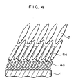
- Thus, as shown in Figure 4, when the nematic liquid crystal (7) comes in contact with this type of substrate formed of a monomolecular film with a nematic crystal portion (6a), the molecules of the nematic liquid crystal (7) insert themselves into the space in the nematic crystal portion (6a), resulting in an excellent control of the overall liquid crystal orientation. Further, (4a) and (6a) shown in Figure 4 are conceptional indications of the short carbon chain (4) and the nematic liquid crystal portion (6) shown in Figure 3.
- Moreover, as shown in Figure 5, when the liquid crystal molecules to be sealed are ferroelectric liquid crystal, if the silane-type surfactant bonded to the ferroelectric liquid crystal portion (8) and the silane-type surfactant with a short hydrocarbon chain (4) are adsorbed in specified proportions, an alignment film for liquid crystal consisting of monomolecular film can be produced. Also, as shown in Figure 6, when the ferroelectric liquid crystal (9) comes in contact with a substrate with a monomolecular film containing this type of ferroelectric liquid crystal portion (8a), the ferroelectric liquid crystal molecules (9) insert themselves into the gaps in the ferroelectric liquid crystal portion (8a) of the monomolecular film, resulting in excellent control of the overall liquid crystal orientation. Further, (4a) and (8a) shown in Figure 6 are conceptional indications of the short carbon chain (4) and the nematic liquid crystal portion (8) shown in Figure 5.
- The examples described above are the most representative cases of alignment film for liquid crystal in which multiple silane-type surfactants mixed in specified proportions are concurrently chemisorbed, and of an alignment film for liquid crystal consisting of monomolecular film formed of a silane-type surfactant bonded to liquid crystal molecules and a silane-type surfactant with a short hydrocarbon chain which are adsorbed in specified proportions; however, in cases where an alignment film for liquid crystal is formed, through adsorption of only a silane-type surfactant with long linear hydrocarbon chains, an alignment film for liquid crystal able to orient the aforementioned liquid crystal almost perpendicularly is produced.
- As an example, Figure 9 shows the spectrum data measured by FTIR spectroscopy of an alignment film produced through adsorption compared to that of an alignment film produced by the conventional spin-coating method.
- The test compound used here was CH₂=CH-(CH₂-)₁₇-SiCl₃; in the alignment film produced by adsorption (A), the adsorptions of 2930 cm⁻¹ and 2860 cm⁻¹ were clearly split, but in the spin-coated oriented film (B), two adsorption peaks overlapped; thus it was determined that the hydrocarbon chain is oriented almost perpendicularly to the substrate in the adsorbed monomolecular film, but the orientation in the spin-coated film was irregular at the molecular level.
- As shown in Figure 7, when producing a liquid crystal display unit using an alignment film for liquid crystal comprising monomolecular film of two types of silane-type compounds with different linear hydrocarbon chain lengths, silane-type surfactants which can efficiently control the orientation of long molecules dissolved in n-cetane are chemisorbed onto the second substrate (16), on which a matrix has been formed in advance; thereby single layers of monomolecular film for alignment film for liquid crystal (17) are formed onto the surface of the aforementioned substrate through the chemical bonding between the silicone in the aforementioned silane-type surfactants and the -OH group in the natural oxidization film on the surface of the aforementioned substrate. Next, the aforementioned first substrate (13) is installed facing the second substrate (16) across the spacer (18), and then fixed using adhesive (19). Next, the specified liquid crystal (20) is inserted between the aforementioned first substrate (13) and the second substrate (16). It is then completed by assembling the polarizers (21) and (22). With this type of liquid crystal display unit, a picture image can be displayed in the direction of the arrow (A) by driving various transistors using video signals while irradiating the entire surface with the back light (23).
- As described above, because the alignment film for liquid crystal of this invention is structured by the direct monomolecular chemisorption of silane-type surfactants onto the surface of the substrate, it is efficient, uniform, and thin; further, it has the ability to improve the controlling characteristics of the liquid crystal molecule orientation.
- Moreover, by using silane-type surfactants with molecules bonded to the liquid crystal molecules, the controlling characteristics of the orientation is further improved.
- Also, in liquid crystal display units using the oriented film for liquid crystal of this invention, the insulating film between the liquid crystal and the electrode is extremely thin; therefore, the energy requirements to drive the liquid crystal display unit can be reduced.
- Further, because the alignment film produced by the process of this invention, as well as liquid crystal cells using this alignment film, have the ability to line up the molecules with large intramolecular dipoles in a specific direction, extremely large secondary nonlinear optical effects can be generated.
Claims (29)
Priority Applications (1)
| Application Number | Priority Date | Filing Date | Title |
|---|---|---|---|
| EP94116585A EP0635747B1 (en) | 1989-03-09 | 1990-03-09 | Alignment film for liquid crystal and method for production thereof |
Applications Claiming Priority (2)
| Application Number | Priority Date | Filing Date | Title |
|---|---|---|---|
| JP5700489 | 1989-03-09 | ||
| JP57004/89 | 1989-03-09 |
Related Child Applications (2)
| Application Number | Title | Priority Date | Filing Date |
|---|---|---|---|
| EP94116585.4 Division-Into | 1990-03-09 | ||
| EP94116585A Division EP0635747B1 (en) | 1989-03-09 | 1990-03-09 | Alignment film for liquid crystal and method for production thereof |
Publications (3)
| Publication Number | Publication Date |
|---|---|
| EP0386782A2 true EP0386782A2 (en) | 1990-09-12 |
| EP0386782A3 EP0386782A3 (en) | 1991-08-07 |
| EP0386782B1 EP0386782B1 (en) | 1996-07-24 |
Family
ID=13043323
Family Applications (2)
| Application Number | Title | Priority Date | Filing Date |
|---|---|---|---|
| EP94116585A Expired - Lifetime EP0635747B1 (en) | 1989-03-09 | 1990-03-09 | Alignment film for liquid crystal and method for production thereof |
| EP90104531A Expired - Lifetime EP0386782B1 (en) | 1989-03-09 | 1990-03-09 | Alignment film for liquid crystal and method for production thereof, as well as liquid crystal display device utilizing said alignment film and method for production thereof |
Family Applications Before (1)
| Application Number | Title | Priority Date | Filing Date |
|---|---|---|---|
| EP94116585A Expired - Lifetime EP0635747B1 (en) | 1989-03-09 | 1990-03-09 | Alignment film for liquid crystal and method for production thereof |
Country Status (3)
| Country | Link |
|---|---|
| US (2) | US5133895A (en) |
| EP (2) | EP0635747B1 (en) |
| DE (2) | DE69033571T2 (en) |
Cited By (12)
| Publication number | Priority date | Publication date | Assignee | Title |
|---|---|---|---|---|
| EP0476543A2 (en) * | 1990-09-17 | 1992-03-25 | Matsushita Electric Industrial Co., Ltd. | Liquid crystal alignment film and method of manufacturing the same |
| US5155610A (en) * | 1990-07-19 | 1992-10-13 | U.S. Philips Corporation | Method of providing a liquid crystalline auxiliary layer in a display cell |
| JPH04356020A (en) * | 1990-09-17 | 1992-12-09 | Matsushita Electric Ind Co Ltd | Liquid crystal oriented film and production thereof as well as liquid crystal display device and production thereof |
| US5256456A (en) * | 1990-09-17 | 1993-10-26 | Matsushita Electric Industrial Co., Ltd. | Liquid crystal alignment film and method of manufacturing the same |
| EP0601895A1 (en) * | 1992-12-11 | 1994-06-15 | Sharp Kabushiki Kaisha | Method for forming an orientation film |
| US5702777A (en) * | 1993-02-26 | 1997-12-30 | Roesch; Norbert | Silane couplers containing cyclic structural elements as alignment films |
| EP1040876A1 (en) * | 1997-11-18 | 2000-10-04 | Matsushita Electric Industrial Co., Ltd. | Process for the production of monomolecular chemisorption film, and processes for the production of liquid crystal alignment films and liquid crystal displays by using the chemisorption film |
| CN103064217A (en) * | 2011-10-20 | 2013-04-24 | 三星显示有限公司 | Liquid crystal display device, alignment film, and method for manufacturing same |
| EP2520972A3 (en) * | 2011-05-02 | 2014-02-19 | Samsung Display Co., Ltd. | Liquid crystal display device alignment film, and method for manufacturing the same |
| US8865274B2 (en) | 2010-04-02 | 2014-10-21 | Samsung Display Co., Ltd. | Liquid crystal display device, alignment film, and methods for manufacturing the same |
| US9057917B2 (en) | 2010-04-02 | 2015-06-16 | Samsung Display Co., Ltd. | Pixel electrode panel, a liquid crystal display panel assembly and methods for manufacturing the same |
| CN105425473A (en) * | 2014-09-12 | 2016-03-23 | 三星显示有限公司 | Liquid crystal display device and method of manufacturing the same |
Families Citing this family (24)
| Publication number | Priority date | Publication date | Assignee | Title |
|---|---|---|---|---|
| US5133895A (en) * | 1989-03-09 | 1992-07-28 | Matsushita Electric Industrial Co., Ltd. | Alignment film for liquid crystal and method for production thereof, as well as liquid crystal display device utilizing said alignment film and method for production thereof |
| JP2711585B2 (en) * | 1990-06-26 | 1998-02-10 | 日本石油株式会社 | Compensator for active matrix liquid crystal display |
| JP3078573B2 (en) * | 1990-11-16 | 2000-08-21 | 株式会社半導体エネルギー研究所 | Liquid crystal electro-optical device |
| US6503567B2 (en) | 1990-12-25 | 2003-01-07 | Matsushita Electric Industrial Co., Ltd. | Transparent substrate and method of manufacturing the same |
| DE69129145T2 (en) | 1990-12-25 | 1998-07-16 | Matsushita Electric Ind Co Ltd | Transparent substrate with applied monomolecular film and process for its production |
| US6051289A (en) * | 1993-02-12 | 2000-04-18 | Nippon Petrochemicals, Co., Ltd | Liquid crystalline polymer film, laminate sheet for optical element using same, and optical element using the laminate |
| JP3517890B2 (en) * | 1993-02-18 | 2004-04-12 | 日産化学工業株式会社 | Coating liquid for insulating film formation for liquid crystal display element |
| US5543949A (en) * | 1993-08-18 | 1996-08-06 | Kabushiki Kaisha Toshiba | LCD polymer orienting film with a dipole moment greater than 20 debye and is bound to the substrate surface through a surface treating agent |
| GB2293889A (en) * | 1994-10-03 | 1996-04-10 | Sharp Kk | Liquid crystal device and method of making a liquid crystal device |
| US5578351A (en) * | 1995-01-20 | 1996-11-26 | Geo-Centers, Inc. | Liquid crystal composition and alignment layer |
| TW515926B (en) | 1996-07-10 | 2003-01-01 | Matsushita Electric Ind Co Ltd | Liquid crystal alignment film and method for producing the same, and liquid crystal display apparatus using the same and method for producing the same |
| DE69717135T2 (en) * | 1996-07-25 | 2003-10-09 | Geo Ct S Inc | LIQUID CRYSTAL COMPOSITION AND ORIENTATION LAYER |
| US6057038A (en) * | 1996-08-02 | 2000-05-02 | Sharp Kabushiki Kaisha | Substrate for use in display element, method of manufacturing the same, and apparatus for manufacturing the same |
| US6816218B1 (en) * | 1997-04-14 | 2004-11-09 | Merck Patent Gmbh | Homeotropically aligned liquid crystal layer and process for the homeotropic alignment of liquid crystals on plastic substrates |
| TW539901B (en) | 1997-07-31 | 2003-07-01 | Matsushita Electric Ind Co Ltd | Chemisorption matter and liquid crystal oriented film and liquid crystal display element using it |
| US6517401B1 (en) | 1997-11-18 | 2003-02-11 | Matsushita Electric Industrial Co., Ltd. | Process for the production of monomolecular chemisorption film, and processes for the production of liquid crystal alignment films and liquid crystal displays by using the chemisorption film |
| TW507106B (en) * | 1998-03-11 | 2002-10-21 | Matsushita Electric Ind Co Ltd | Method for producing an alignment chemisorption monomolecular film |
| EP1084822A1 (en) * | 1999-02-10 | 2001-03-21 | Matsushita Electric Industrial Co., Ltd. | Organic thin films, process for the production thereof and equipment therefor; alignment layers for liquid crystals, process for the production thereof and equipment therefor; and liquid crystal displays made by using the alignment layers and process for the production thereof |
| JP4185678B2 (en) * | 2001-06-08 | 2008-11-26 | 株式会社日立製作所 | Liquid crystal display |
| US7903228B2 (en) * | 2002-01-10 | 2011-03-08 | Kent State University | Material for liquid crystal cell |
| US7758773B2 (en) * | 2002-01-10 | 2010-07-20 | Kent State University | Non-synthetic method for modifying properties of liquid crystals |
| US7051760B1 (en) | 2004-01-30 | 2006-05-30 | Ralph Lewis Beamer | Three-way inline piggable branch valve |
| JP2009223138A (en) * | 2008-03-18 | 2009-10-01 | Seiko Epson Corp | Liquid crystal device and method of manufacturing the same, and electronic apparatus |
| CN105481889B (en) * | 2015-11-17 | 2018-08-14 | 深圳市华星光电技术有限公司 | The production method of response type vertical orientation organosilicon material and liquid crystal display panel |
Citations (4)
| Publication number | Priority date | Publication date | Assignee | Title |
|---|---|---|---|---|
| US3854793A (en) * | 1972-06-27 | 1974-12-17 | Bell Telephone Labor Inc | Liquid crystal cells |
| EP0168242A2 (en) * | 1984-07-10 | 1986-01-15 | Seiko Instruments Inc. | Ferro-electric liquid crystal electro-optical device |
| EP0251548A2 (en) * | 1986-06-25 | 1988-01-07 | AT&T Corp. | Liquid crystal device with chemically-induced high-tilt alignment coating |
| EP0286539A1 (en) * | 1987-04-10 | 1988-10-12 | Commissariat A L'energie Atomique | Bistable smectic ferroelectric liquid-crystal display |
Family Cites Families (21)
| Publication number | Priority date | Publication date | Assignee | Title |
|---|---|---|---|---|
| US3728008A (en) * | 1971-12-01 | 1973-04-17 | Olivetti & Co Spa | Liquid crystal display |
| SU496853A1 (en) * | 1974-07-12 | 1978-10-05 | Предприятие П/Я А-1631 | Method of manufacturing liquid crystal indicators |
| JPS5220847A (en) * | 1975-08-09 | 1977-02-17 | Sharp Corp | Base panel for holding liquid crystal |
| JPS5683718A (en) * | 1979-12-13 | 1981-07-08 | Asahi Glass Co Ltd | Liquid crystal display element |
| JPS578522A (en) * | 1980-06-18 | 1982-01-16 | Hitachi Ltd | Liquid crystal display device |
| JPS5716421A (en) * | 1980-07-02 | 1982-01-27 | Sanyo Electric Co Ltd | Liquid crystal display device |
| JPS5716419A (en) * | 1980-07-02 | 1982-01-27 | Casio Comput Co Ltd | Liquid crystal display device |
| JPS5764725A (en) * | 1980-10-09 | 1982-04-20 | Ricoh Elemex Corp | Plastic substrate liquid crystal display device |
| JPS57195219A (en) * | 1981-05-25 | 1982-11-30 | Matsushita Electric Ind Co Ltd | Liquid crystal color display panel |
| JPS589125A (en) * | 1981-07-10 | 1983-01-19 | Hitachi Ltd | Composition for coating liquid crystal oriented film by printing |
| DE3331515A1 (en) * | 1983-09-01 | 1985-03-21 | Merck Patent Gmbh, 6100 Darmstadt | TRIALKANOYLOXYSILANES |
| NL8402498A (en) * | 1984-08-14 | 1986-03-03 | Philips Nv | IMAGE DISPLAY CELL. |
| DE3601742A1 (en) * | 1985-06-13 | 1987-07-23 | Merck Patent Gmbh | ORGANOSILICIUM COMPOUNDS |
| FR2588970B1 (en) * | 1985-10-23 | 1988-01-15 | Reosc | LIGHT MIRROR WITH NON-FLAT REFLECTIVE FACE, ESPECIALLY TELESCOPE MIRROR |
| US4796979A (en) * | 1986-04-07 | 1989-01-10 | Canon Kabushiki Kaisha | Ferroelectric liquid crystal device having dual laminated alignment films |
| JPS62269119A (en) * | 1986-05-16 | 1987-11-21 | Stanley Electric Co Ltd | Liquid crystal display element |
| DD252449A1 (en) * | 1986-09-04 | 1987-12-16 | Werk Fernsehelektronik Veb | METHOD FOR ORIENTATION OF LIQUID CRYSTALS |
| FI77680C (en) * | 1987-03-25 | 1989-04-10 | K & V Licencing Oy | FOERFARANDE FOER FRAMSTAELLNING AV ETT MEMBRAN MED MONOMOLEKULAER, SYMMETRISK MOLEKYLFOERDELNINGSSTRUKTUR. |
| US5133895A (en) * | 1989-03-09 | 1992-07-28 | Matsushita Electric Industrial Co., Ltd. | Alignment film for liquid crystal and method for production thereof, as well as liquid crystal display device utilizing said alignment film and method for production thereof |
| EP0476543B1 (en) * | 1990-09-17 | 1996-08-28 | Matsushita Electric Industrial Co., Ltd. | Liquid crystal alignment film and method of manufacturing the same |
| US5256456A (en) * | 1990-09-17 | 1993-10-26 | Matsushita Electric Industrial Co., Ltd. | Liquid crystal alignment film and method of manufacturing the same |
-
1990
- 1990-03-05 US US07/489,248 patent/US5133895A/en not_active Expired - Lifetime
- 1990-03-09 DE DE69033571T patent/DE69033571T2/en not_active Expired - Lifetime
- 1990-03-09 DE DE69027875T patent/DE69027875T2/en not_active Expired - Lifetime
- 1990-03-09 EP EP94116585A patent/EP0635747B1/en not_active Expired - Lifetime
- 1990-03-09 EP EP90104531A patent/EP0386782B1/en not_active Expired - Lifetime
-
1992
- 1992-03-30 US US07/859,875 patent/US5515190A/en not_active Expired - Lifetime
Patent Citations (4)
| Publication number | Priority date | Publication date | Assignee | Title |
|---|---|---|---|---|
| US3854793A (en) * | 1972-06-27 | 1974-12-17 | Bell Telephone Labor Inc | Liquid crystal cells |
| EP0168242A2 (en) * | 1984-07-10 | 1986-01-15 | Seiko Instruments Inc. | Ferro-electric liquid crystal electro-optical device |
| EP0251548A2 (en) * | 1986-06-25 | 1988-01-07 | AT&T Corp. | Liquid crystal device with chemically-induced high-tilt alignment coating |
| EP0286539A1 (en) * | 1987-04-10 | 1988-10-12 | Commissariat A L'energie Atomique | Bistable smectic ferroelectric liquid-crystal display |
Cited By (17)
| Publication number | Priority date | Publication date | Assignee | Title |
|---|---|---|---|---|
| US5155610A (en) * | 1990-07-19 | 1992-10-13 | U.S. Philips Corporation | Method of providing a liquid crystalline auxiliary layer in a display cell |
| EP0476543A2 (en) * | 1990-09-17 | 1992-03-25 | Matsushita Electric Industrial Co., Ltd. | Liquid crystal alignment film and method of manufacturing the same |
| EP0476543A3 (en) * | 1990-09-17 | 1992-11-19 | Matsushita Electric Industrial Co., Ltd. | Liquid crystal alignment film and method of manufacturing the same |
| JPH04356020A (en) * | 1990-09-17 | 1992-12-09 | Matsushita Electric Ind Co Ltd | Liquid crystal oriented film and production thereof as well as liquid crystal display device and production thereof |
| US5256456A (en) * | 1990-09-17 | 1993-10-26 | Matsushita Electric Industrial Co., Ltd. | Liquid crystal alignment film and method of manufacturing the same |
| EP0601895A1 (en) * | 1992-12-11 | 1994-06-15 | Sharp Kabushiki Kaisha | Method for forming an orientation film |
| US5468519A (en) * | 1992-12-11 | 1995-11-21 | Sharp Kabushiki Kaisha | Method for forming an orientation film including coupling an organic compound to a silane coupling agent in a magnetic or electrical field |
| US5702777A (en) * | 1993-02-26 | 1997-12-30 | Roesch; Norbert | Silane couplers containing cyclic structural elements as alignment films |
| EP1040876A1 (en) * | 1997-11-18 | 2000-10-04 | Matsushita Electric Industrial Co., Ltd. | Process for the production of monomolecular chemisorption film, and processes for the production of liquid crystal alignment films and liquid crystal displays by using the chemisorption film |
| EP1040876A4 (en) * | 1997-11-18 | 2004-05-26 | Matsushita Electric Ind Co Ltd | Process for the production of monomolecular chemisorption film, and processes for the production of liquid crystal alignment films and liquid crystal displays by using the chemisorption film |
| US8865274B2 (en) | 2010-04-02 | 2014-10-21 | Samsung Display Co., Ltd. | Liquid crystal display device, alignment film, and methods for manufacturing the same |
| US9057917B2 (en) | 2010-04-02 | 2015-06-16 | Samsung Display Co., Ltd. | Pixel electrode panel, a liquid crystal display panel assembly and methods for manufacturing the same |
| US9081237B2 (en) | 2010-04-02 | 2015-07-14 | Samsung Display Co., Ltd. | Pixel electrode panel, a liquid crystal display panel assembly and methods for manufacturing the same |
| EP2520972A3 (en) * | 2011-05-02 | 2014-02-19 | Samsung Display Co., Ltd. | Liquid crystal display device alignment film, and method for manufacturing the same |
| CN103064217A (en) * | 2011-10-20 | 2013-04-24 | 三星显示有限公司 | Liquid crystal display device, alignment film, and method for manufacturing same |
| US9723769B2 (en) | 2011-10-20 | 2017-08-01 | Samsung Display Co., Ltd. | Liquid crystal display device, alignment film, and methods for manufacturing the same |
| CN105425473A (en) * | 2014-09-12 | 2016-03-23 | 三星显示有限公司 | Liquid crystal display device and method of manufacturing the same |
Also Published As
| Publication number | Publication date |
|---|---|
| EP0635747A1 (en) | 1995-01-25 |
| EP0386782B1 (en) | 1996-07-24 |
| DE69033571D1 (en) | 2000-08-03 |
| US5133895A (en) | 1992-07-28 |
| DE69027875T2 (en) | 1997-02-27 |
| EP0386782A3 (en) | 1991-08-07 |
| DE69027875D1 (en) | 1996-08-29 |
| US5515190A (en) | 1996-05-07 |
| DE69033571T2 (en) | 2001-03-01 |
| EP0635747B1 (en) | 2000-06-28 |
Similar Documents
| Publication | Publication Date | Title |
|---|---|---|
| EP0386782A2 (en) | Alignment film for liquid crystal and method for production thereof, as well as liquid crystal display device utilizing said alignment film and method for production thereof | |
| EP0476543B1 (en) | Liquid crystal alignment film and method of manufacturing the same | |
| US7182830B2 (en) | Compositions and assembly process for liquid crystal display | |
| US5948316A (en) | Liquid crystal composition and alignment layer | |
| US6852374B2 (en) | Liquid crystal display device, optical element, method of fabricating the liquid crystal display device and method of making the optical element | |
| KR940001825Y1 (en) | Liquid crystal display devices | |
| US6156232A (en) | Liquid crystal composition and alignment layer | |
| KR20010024339A (en) | Liquid crystal alignment film and method of producing the same, and liquid crystal display using the same and method of producing the same | |
| US5256456A (en) | Liquid crystal alignment film and method of manufacturing the same | |
| CN109471303A (en) | Liquid crystal disply device and its preparation method | |
| JP2558903B2 (en) | Liquid crystal alignment film, manufacturing method thereof, and liquid crystal display device using the same | |
| JP3083477B2 (en) | Liquid crystal alignment film, method of manufacturing the same, and liquid crystal display device using the same | |
| Ohtake et al. | A liquid crystal display having a rubbing-free photo-aligned monomolecular layer as an alignment film | |
| JP3161645B2 (en) | Liquid crystal alignment film, method of manufacturing the same, and liquid crystal display device | |
| JP3301960B2 (en) | Liquid crystal alignment film, method for manufacturing liquid crystal alignment film, liquid crystal display device, and method for manufacturing liquid crystal display device | |
| JP3537709B2 (en) | Liquid crystal alignment film and liquid crystal display device using the same | |
| JPH10339876A (en) | Liquid crystal alignment layer, manufacture therefor, liquid crystal display device using the same and manufacture therefor | |
| KR20010030786A (en) | Liquid crystal alignment film and method of producing the same, and liquid crystal display using the same and method of producing the same | |
| JP3497119B2 (en) | Organic thin film and manufacturing method thereof, liquid crystal alignment film and manufacturing method thereof, and liquid crystal display device and manufacturing method thereof | |
| JPS61151617A (en) | Liquid crystal light valve | |
| KR19980051661A (en) | Display device using potassium iodide aqueous solution | |
| JPH02257122A (en) | Method for orienting liquid crystal |
Legal Events
| Date | Code | Title | Description |
|---|---|---|---|
| PUAI | Public reference made under article 153(3) epc to a published international application that has entered the european phase |
Free format text: ORIGINAL CODE: 0009012 |
|
| AK | Designated contracting states |
Kind code of ref document: A2 Designated state(s): DE FR GB |
|
| 17P | Request for examination filed |
Effective date: 19901228 |
|
| PUAL | Search report despatched |
Free format text: ORIGINAL CODE: 0009013 |
|
| AK | Designated contracting states |
Kind code of ref document: A3 Designated state(s): DE FR GB |
|
| 17Q | First examination report despatched |
Effective date: 19930604 |
|
| GRAH | Despatch of communication of intention to grant a patent |
Free format text: ORIGINAL CODE: EPIDOS IGRA |
|
| GRAH | Despatch of communication of intention to grant a patent |
Free format text: ORIGINAL CODE: EPIDOS IGRA |
|
| GRAA | (expected) grant |
Free format text: ORIGINAL CODE: 0009210 |
|
| AK | Designated contracting states |
Kind code of ref document: B1 Designated state(s): DE FR GB |
|
| XX | Miscellaneous (additional remarks) |
Free format text: TEILANMELDUNG 94116585.4 EINGEREICHT AM 09/03/90. |
|
| REF | Corresponds to: |
Ref document number: 69027875 Country of ref document: DE Date of ref document: 19960829 |
|
| ET | Fr: translation filed | ||
| RIN2 | Information on inventor provided after grant (corrected) |
Free format text: OGAWA, KAZUFUMI * MINO, NORIHISA * TAMURA, HIDEHARU |
|
| PLBE | No opposition filed within time limit |
Free format text: ORIGINAL CODE: 0009261 |
|
| STAA | Information on the status of an ep patent application or granted ep patent |
Free format text: STATUS: NO OPPOSITION FILED WITHIN TIME LIMIT |
|
| 26N | No opposition filed | ||
| REG | Reference to a national code |
Ref country code: GB Ref legal event code: IF02 |
|
| PGFP | Annual fee paid to national office [announced via postgrant information from national office to epo] |
Ref country code: GB Payment date: 20090304 Year of fee payment: 20 |
|
| PGFP | Annual fee paid to national office [announced via postgrant information from national office to epo] |
Ref country code: DE Payment date: 20090306 Year of fee payment: 20 |
|
| PGFP | Annual fee paid to national office [announced via postgrant information from national office to epo] |
Ref country code: FR Payment date: 20090316 Year of fee payment: 20 |
|
| REG | Reference to a national code |
Ref country code: GB Ref legal event code: PE20 Expiry date: 20100308 |
|
| PG25 | Lapsed in a contracting state [announced via postgrant information from national office to epo] |
Ref country code: GB Free format text: LAPSE BECAUSE OF EXPIRATION OF PROTECTION Effective date: 20100308 |
|
| PG25 | Lapsed in a contracting state [announced via postgrant information from national office to epo] |
Ref country code: DE Free format text: LAPSE BECAUSE OF EXPIRATION OF PROTECTION Effective date: 20100309 |