EP0385702A2 - Elektrisches Verfahren, um Positionsfehler an den Kontaktöffnungen in einer Halbleitervorrichtung zu erkennen - Google Patents
Elektrisches Verfahren, um Positionsfehler an den Kontaktöffnungen in einer Halbleitervorrichtung zu erkennen Download PDFInfo
- Publication number
- EP0385702A2 EP0385702A2 EP90302042A EP90302042A EP0385702A2 EP 0385702 A2 EP0385702 A2 EP 0385702A2 EP 90302042 A EP90302042 A EP 90302042A EP 90302042 A EP90302042 A EP 90302042A EP 0385702 A2 EP0385702 A2 EP 0385702A2
- Authority
- EP
- European Patent Office
- Prior art keywords
- contact hole
- layer
- short
- conductor pattern
- circuit
- Prior art date
- Legal status (The legal status is an assumption and is not a legal conclusion. Google has not performed a legal analysis and makes no representation as to the accuracy of the status listed.)
- Granted
Links
Images

Classifications
-
- H—ELECTRICITY
- H10—SEMICONDUCTOR DEVICES; ELECTRIC SOLID-STATE DEVICES NOT OTHERWISE PROVIDED FOR
- H10P—GENERIC PROCESSES OR APPARATUS FOR THE MANUFACTURE OR TREATMENT OF DEVICES COVERED BY CLASS H10
- H10P74/00—Testing or measuring during manufacture or treatment of wafers, substrates or devices
- H10P74/20—Testing or measuring during manufacture or treatment of wafers, substrates or devices characterised by the properties tested or measured, e.g. structural or electrical properties
- H10P74/203—Structural properties, e.g. testing or measuring thicknesses, line widths, warpage, bond strengths or physical defects
Definitions
- the present invention relates to an examination method for a semiconductor device manufacturing process, and more specifically to a method for detecting a positional deviation of a contact hole which is formed in an interlayer insulator layer to mutually connect a pair of conducting layers separated from each other by the interlayer insulator layer.
- Another object of the present invention is to provide a method for detecting a deviation of a formed contact hole, without a visual inspection using an optical microscope.
- a still further object of the present invention is to provide a method for detecting a deviation of a formed contact hole, by an electrical property measurement which can be performed in an automatic manner.
- a method for detecting a positional deviation of a contact hole which is formed in an interlayer insulator layer to mutually connect a pair of conducting layers separated from each other by the interlayer insulator layer comprising the steps of forming a detection conductor pattern on a substrate at a peripheral portion of a contact hole formation area in which a contact hole is to be formed, forming a first insulating layer to cover the detection conductor pattern, forming a first conducting layer of a predetermined pattern on the first insulating layer so as to cover the contact hole formation area, forming a second insulating layer to cover the first conducting layer, forming a contact hole in the second insulating layer at the contact hole formation area, forming a second conducting layer on the second insulation layer so that the second conducting layer is deposited within the contact hole, and detecting a short-circuit between the detection conductor pattern and one of the first and second conducting layers.
- the contact hole is formed in the second insulation layer
- the formed contact hole would partially or entirely offset from a peripheral edge of the first or lower conducting layer, and therefore, a hole would be formed in the first insulating layer to reach the detection conductor pattern on one hand and to communicate with the contact hole formed in the second insulating layer on the other hand. Therefore, the second conducting layer formed on the second insulating layer will be deposited not only within the contact hole formed in the second insulating layer so as to contact the first conducting layer but also within the hole formed in the first insulating layer so as to contact the detection conductor pattern. As a result, the detection conductor pattern is brought into an electric contact with the first conducting layer and the second conducting layer. Accordingly, an adverse positional deviation of the formcd contact hole can be known by detecting a short-circuit between the detection conductor pattern and the first conducting layer or between the detection conductor pattern and the second conducting layer.
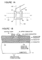
- FIG. 1A and 1B there are shown a diagrammatic plan view of a semiconductor device formed with one embodiment of a contact hole deviation checking conductor pattern in accordance with the present invention, in the case of no adverse deviation of the contact hole, and a diagrammatic sectional view taken along the line I-I in Figure 1A.
- the shown device includes a silicon substrate 10 and a first insulating layer 12 formed to cover an upper surface of the silicon substrate 10.
- a contact hole deviation checking conductor pattern composed of four strip-shaped detection conductors 14A, 14B, 14C and 14D, each of whoch is formed to extend outwardly radially from a position slightly separated from a corresponding side of a rectangular contact hole formation area 16 in a plan view, as seen from Figure 1A.
- the strip-shaped detection conductors 14A, 14B, 14C and 14D are located at equal angular intervals with regard to a center of the contact hole formation area 16, and extend in four directions orthogonal to one another in the shown embodiment.
- an edge of each of the detection conductors 14A, 14B, 14C and 14D near to the contact hole formation area 16 is separate from an outer edge of the contact hole formation area 16 by some distance which corresponds to, for example, a maximum admissible amount of a positional deviation of a contact hole.
- a second insulating layer 18 is deposited to cover the detection conductors 14A, 14B, 14C and 14D and a portion of the first insulating layer 12 on which the detection conductors 14A, 14B, 14C and 14D are not formed.
- a first or lower conducting layer 20 is formed and patterned in alignment with but larger in size than the contact hole formation area 16 in a plan view, as seen from Figure 1A.
- a peripheral portion of the lower conducting layer 20 partially overlaps with each of the detection conductors 14A, 14B, 14C and 14D in a plan view, as also seen from Figures 1A and 1B.
- a third insulating layer 22 is deposited to cover the lower conducting layer 20 and a portion of the second insulating layer 18 on which the lower conducting layer 20 is not formed. This third insulating layer 22 serves as an interlayer insulator.
- a contact hole 24 is formed in conformity with or in matching with the contact hole formation area 16 to pierce through the interlayer insulating layer 22.
- the size of the contact hole 24 is sufficiently smaller than that of the lower conducting layer 20. Therefore, if the formed contact hole 24 does not deviate from the contact hole formation area 16, namely, is in alignment with the contact hole formation area 16, an etching for formation of the contact hole 24 in blocked by the lower conducting layer 20. In other words, the contact hole 24 is positioned on only the lower conducting layer 20.
- a second or upper conducting layer 26 is formed to fulfil in the contact hole 24 and patterned to form a desired wiring conductor.
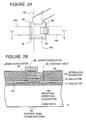
- the formation position of the contact hole 24 substantially deviates as shown in Figures 2A and 2B, namely if the contact hole 24 is formed to partially protrude out of the lower conducting layer 20 the etching for formation of the contact hole is not completely blocked by the lower conducting layer 20, and the second insulating layer 18 between the detection conductor 14A and the lower conducting layer 20 are partially removed so that the contact hole 24 partially reaches to the detection conductor 14A.
- the upper conducting layer 26 having filled in the contact hole 24 has a portion 28 short-circuiting between the upper conducting layer 26 and the detection conductor 14A.
- the short-circuit between the upper conducting layer 26 and the detection conductor 14A can be known in an electric measurement manner. If a short-circuit can be detected between the upper conducting layer 26 and any one of the detection conductors 14A, 14B, 14C and 14D, it can be concluded that the formed contact hole 24 deviates from a proper formation position.
- a short-circuit also occur between the upper conducting layer 26 and the detection conductors 14A, 14B, 14C and 14D. Therefore, whether or not the formed contact hole has a desired size, namely, a size of the formed contact hole can be known by detecting a short-circuit between the upper conducting layer 26 and all the detection conductors 14A, 14B, 14C and 14D.
- the short-circuit has been detected between the upper conducting layer 26 and the detection conductors 14A, 14B, 14C and 14D.
- the short-circuit can been detected between the lower conducting layer 20 and the detection conductors 14A, 14B, 14C and 14D, as seen from Figure 2B.
- the upper conducting layer 26 and the detection conductor 14A are short-circuited. Since there are provided the four detection conductors 14A, 14B, 14C and 14D separate from one another and orthogonal to one another, a direction of the positional deviation of the contact hole can be determined by inspecting which of the four detection conductors 14A, 14B, 14C and 14D short-circuits with the upper conducting layer 26. In the above mentioned example shown in Figure 2A, it can be judged on the basis of the short-circuit between the upper conducting layer 26 and the detection conductor 14A that the contact hole 24 has deviated in a right-hand direction of the proper formation position.
- the four detection conductors 14A, 14B, 14C and 14D can he replaced with a single detection conductor which extends to surround the contact hole formation area.
- FIG. 3 there is shown a diagrammatic plan view of a semiconductor device formed with another embodiment of a contact hole deviation checking conductor pattern in accordance with the present invention, in the case of no adverse deviation of the contact hole.
- each detection conductor 14A, 14B, 14C or 14D formed in proximity with each side of the rectangular contact hole formation area 16 are divided into three separate sub-conductors 30A, 30B and 30C (32A, 32B and 32C, 34A, 34B and 34C, and 36A, 36B and 36C) which extend in parallel to the side concerned of the rectangular contact hole formation area 16, separately from the side concerned of the rectangular contact hole formation area 16 by different distances in a direction perpendicular to the side concerned of the rectangular contact hole formation area 16.
- the lower conducting layer 20 is formed to partially overlap with an innermost one of the three separate sub-conductors 30A, 32A, 34A, and 36A, and the upper conducting layer is formed to have a size sufficient to at least partially with an outermost one of the three separate sub-conductors 30C, 32C, 34C, and 36C.
- the amount of the positional deviation of the contact hole can be known by detecting which of the four detection conductors short-circuits with the upper or lower conducting layer 20 or 26 and by detecting which of the three sub-conductors (for example, 30A, 30B and 30C) short-circuits with the upper or lower conducting layer 20 or 26.
- the detection conductors or subconductors can be formed of wiring conductors necessary to operation of the semiconductor device
- the detection conductor is formed at a position slightly separate from a contact hole formation area and at a level lower or deeper than a level at which a bottom of a contact hole is to be positioned.
- An electrical short-circuit between the detection conductor and the upper or lower conducting layer is detected for knowing a positional deviation of the formed contact hole.
- the positional deviation of the formed contact hole can be detected in an electric manner, it is possible to greatly elevate the efficiency for checking the positional deviation of the formed contact hole.
Landscapes
- Internal Circuitry In Semiconductor Integrated Circuit Devices (AREA)
- Testing Or Measuring Of Semiconductors Or The Like (AREA)
- Testing Of Individual Semiconductor Devices (AREA)
Applications Claiming Priority (3)
| Application Number | Priority Date | Filing Date | Title |
|---|---|---|---|
| JP1047781A JP2890442B2 (ja) | 1989-02-27 | 1989-02-27 | 半導体装置のコンタクトホールの目ずれ検査方法 |
| JP47781/89 | 1989-02-27 | ||
| JP4778189 | 1989-02-27 |
Publications (3)
| Publication Number | Publication Date |
|---|---|
| EP0385702A2 true EP0385702A2 (de) | 1990-09-05 |
| EP0385702A3 EP0385702A3 (de) | 1991-01-02 |
| EP0385702B1 EP0385702B1 (de) | 1999-12-08 |
Family
ID=12784914
Family Applications (1)
| Application Number | Title | Priority Date | Filing Date |
|---|---|---|---|
| EP90302042A Expired - Lifetime EP0385702B1 (de) | 1989-02-27 | 1990-02-27 | Elektrisches Verfahren, um Positionsfehler an den Kontaktöffnungen in einer Halbleitervorrichtung zu erkennen |
Country Status (4)
| Country | Link |
|---|---|
| US (1) | US5066908A (de) |
| EP (1) | EP0385702B1 (de) |
| JP (1) | JP2890442B2 (de) |
| DE (1) | DE69033386T2 (de) |
Cited By (2)
| Publication number | Priority date | Publication date | Assignee | Title |
|---|---|---|---|---|
| WO2006091990A1 (de) * | 2005-03-01 | 2006-09-08 | At & S Austria Technologie & Systemtechnik Aktiengesellschaft | Mehrlagige leiterplatte mit leitenden testflächen sowie verfahren zum bestimmen eines versatzes einer innenlage |
| WO2009112456A1 (de) * | 2008-03-13 | 2009-09-17 | X-Fab Semiconductor Foundries Ag | Teststrukturen zur ueberpruefung der positioniergenauigkeit bei mikroelektronischen schaltkreisen |
Families Citing this family (6)
| Publication number | Priority date | Publication date | Assignee | Title |
|---|---|---|---|---|
| US6429670B2 (en) * | 1995-07-18 | 2002-08-06 | Murata Manufacturing Co., Ltd. | Method of examining posture of an electronic part |
| DE19834025A1 (de) * | 1998-07-28 | 2000-02-03 | Aventis Res & Tech Gmbh & Co | Mikrokapseln hergestellt aus Cycloolefinpolymeren oder Cycloolefincopolymeren und deren Verwendung zur kontrollierten Wirkstoffabgabe |
| US6297458B1 (en) | 1999-04-14 | 2001-10-02 | Dell Usa, L.P. | Printed circuit board and method for evaluating the inner layer hole registration process capability of the printed circuit board manufacturing process |
| CN115602663A (zh) * | 2021-07-09 | 2023-01-13 | 长鑫存储技术有限公司(Cn) | 电学测试结构、半导体结构及电学测试方法 |
| US11854915B2 (en) * | 2021-07-09 | 2023-12-26 | Changxin Memory Technologies, Inc. | Electrical test structure, semiconductor structure and electrical test method |
| CN114383491B (zh) * | 2021-11-26 | 2024-12-10 | 广州美维电子有限公司 | 机械钻孔的快速偏位检查方法 |
Family Cites Families (5)
| Publication number | Priority date | Publication date | Assignee | Title |
|---|---|---|---|---|
| US3301939A (en) * | 1963-12-30 | 1967-01-31 | Prec Circuits Inc | Multilayer circuit boards with plated through holes |
| US3859711A (en) * | 1973-03-20 | 1975-01-14 | Ibm | Method of detecting misregistration of internal layers of a multilayer printed circuit panel |
| US4510446A (en) * | 1982-11-03 | 1985-04-09 | Burroughs Corporation | Test coupons for determining the registration of subsurface layers in a multilayer printed circuit board |
| JPS59188144A (ja) * | 1983-04-08 | 1984-10-25 | Hitachi Ltd | 多層配線の形成法 |
| US4894606A (en) * | 1988-07-07 | 1990-01-16 | Paur Tom R | System for measuring misregistration of printed circuit board layers |
-
1989
- 1989-02-27 JP JP1047781A patent/JP2890442B2/ja not_active Expired - Lifetime
-
1990
- 1990-02-27 US US07/485,719 patent/US5066908A/en not_active Expired - Fee Related
- 1990-02-27 EP EP90302042A patent/EP0385702B1/de not_active Expired - Lifetime
- 1990-02-27 DE DE69033386T patent/DE69033386T2/de not_active Expired - Fee Related
Cited By (3)
| Publication number | Priority date | Publication date | Assignee | Title |
|---|---|---|---|---|
| WO2006091990A1 (de) * | 2005-03-01 | 2006-09-08 | At & S Austria Technologie & Systemtechnik Aktiengesellschaft | Mehrlagige leiterplatte mit leitenden testflächen sowie verfahren zum bestimmen eines versatzes einer innenlage |
| CN101133689B (zh) * | 2005-03-01 | 2010-04-21 | At&S奥地利科技及系统技术股份公司 | 具有导电测试面的多层印刷电路板和确定内层错位的方法 |
| WO2009112456A1 (de) * | 2008-03-13 | 2009-09-17 | X-Fab Semiconductor Foundries Ag | Teststrukturen zur ueberpruefung der positioniergenauigkeit bei mikroelektronischen schaltkreisen |
Also Published As
| Publication number | Publication date |
|---|---|
| US5066908A (en) | 1991-11-19 |
| JP2890442B2 (ja) | 1999-05-17 |
| JPH02224354A (ja) | 1990-09-06 |
| DE69033386D1 (de) | 2000-01-13 |
| EP0385702B1 (de) | 1999-12-08 |
| DE69033386T2 (de) | 2000-03-30 |
| EP0385702A3 (de) | 1991-01-02 |
Similar Documents
| Publication | Publication Date | Title |
|---|---|---|
| US6717263B2 (en) | Semiconductor device having contact opening smaller than test probe, and manufacturing process and inspecting method thereof | |
| US6842028B2 (en) | Apparatus for testing reliability of interconnection in integrated circuit | |
| KR100361121B1 (ko) | 반도체 장치 및 그 제조 방법 | |
| US8508055B2 (en) | Semiconductor device and manufacturing method thereof | |
| US20050051902A1 (en) | Semiconductor substrate and test pattern for the same | |
| US5066908A (en) | Method for electrically detecting positional deviation of contact hole in semiconductor device | |
| US4751458A (en) | Test pads for integrated circuit chips | |
| CN120749105B (zh) | 一种半导体测试结构及其测试方法 | |
| JP2718380B2 (ja) | 半導体装置の電気特性検査パターン及び検査方法 | |
| US6081040A (en) | Semiconductor device having alignment mark | |
| EP0325269B1 (de) | Leitende Muster für den elektrischen Test von Halbleiterbausteinen | |
| KR100414223B1 (ko) | 집적 회로 배선의 절연 신뢰성 검사 장치 | |
| US20070210306A1 (en) | Test pattern for measuring contact short at first metal level | |
| US11906577B2 (en) | Pad structure and testkey structure and testing method for semiconductor device | |
| CN118763071A (zh) | 中介层及其测试方法、半导体结构 | |
| US8487305B2 (en) | Semiconductor device and method of manufacturing the same | |
| JP2012109402A (ja) | 半導体装置、半導体装置の製造方法、及び半導体装置の検査方法 | |
| KR100816192B1 (ko) | 정렬 마크를 가지는 반도체 장치 | |
| KR20000045895A (ko) | 테스트패턴 형성방법 | |
| CN115132602A (zh) | 一种半导体测试器件及其制备方法 | |
| KR100369349B1 (ko) | 지문인식용 집적소자 | |
| JP2891729B2 (ja) | 誘電体分離基板の測定方法及びその測定装置 | |
| CN118398599A (zh) | 漏电检测结构及接触结构制作工艺的优化方法 | |
| JPH05198614A (ja) | 半導体チップ,回路基板およびフェースダウンボンディング方法 | |
| JPH10284560A (ja) | 半導体装置の検査方法 |
Legal Events
| Date | Code | Title | Description |
|---|---|---|---|
| PUAI | Public reference made under article 153(3) epc to a published international application that has entered the european phase |
Free format text: ORIGINAL CODE: 0009012 |
|
| 17P | Request for examination filed |
Effective date: 19900313 |
|
| AK | Designated contracting states |
Kind code of ref document: A2 Designated state(s): DE FR GB |
|
| PUAL | Search report despatched |
Free format text: ORIGINAL CODE: 0009013 |
|
| AK | Designated contracting states |
Kind code of ref document: A3 Designated state(s): DE FR GB |
|
| 17Q | First examination report despatched |
Effective date: 19931110 |
|
| GRAG | Despatch of communication of intention to grant |
Free format text: ORIGINAL CODE: EPIDOS AGRA |
|
| GRAG | Despatch of communication of intention to grant |
Free format text: ORIGINAL CODE: EPIDOS AGRA |
|
| GRAH | Despatch of communication of intention to grant a patent |
Free format text: ORIGINAL CODE: EPIDOS IGRA |
|
| GRAH | Despatch of communication of intention to grant a patent |
Free format text: ORIGINAL CODE: EPIDOS IGRA |
|
| GRAA | (expected) grant |
Free format text: ORIGINAL CODE: 0009210 |
|
| AK | Designated contracting states |
Kind code of ref document: B1 Designated state(s): DE FR GB |
|
| REF | Corresponds to: |
Ref document number: 69033386 Country of ref document: DE Date of ref document: 20000113 |
|
| ET | Fr: translation filed | ||
| PLBE | No opposition filed within time limit |
Free format text: ORIGINAL CODE: 0009261 |
|
| STAA | Information on the status of an ep patent application or granted ep patent |
Free format text: STATUS: NO OPPOSITION FILED WITHIN TIME LIMIT |
|
| 26N | No opposition filed | ||
| PGFP | Annual fee paid to national office [announced via postgrant information from national office to epo] |
Ref country code: FR Payment date: 20010213 Year of fee payment: 12 |
|
| PGFP | Annual fee paid to national office [announced via postgrant information from national office to epo] |
Ref country code: GB Payment date: 20010221 Year of fee payment: 12 Ref country code: DE Payment date: 20010221 Year of fee payment: 12 |
|
| REG | Reference to a national code |
Ref country code: GB Ref legal event code: IF02 |
|
| PG25 | Lapsed in a contracting state [announced via postgrant information from national office to epo] |
Ref country code: GB Free format text: LAPSE BECAUSE OF NON-PAYMENT OF DUE FEES Effective date: 20020227 |
|
| PG25 | Lapsed in a contracting state [announced via postgrant information from national office to epo] |
Ref country code: DE Free format text: LAPSE BECAUSE OF NON-PAYMENT OF DUE FEES Effective date: 20020903 |
|
| GBPC | Gb: european patent ceased through non-payment of renewal fee |
Effective date: 20020227 |
|
| PG25 | Lapsed in a contracting state [announced via postgrant information from national office to epo] |
Ref country code: FR Free format text: LAPSE BECAUSE OF NON-PAYMENT OF DUE FEES Effective date: 20021031 |
|
| REG | Reference to a national code |
Ref country code: FR Ref legal event code: ST |