EP0385389A2 - Semiconductor integrated circuit memory enabling memory write masking - Google Patents
Semiconductor integrated circuit memory enabling memory write masking Download PDFInfo
- Publication number
- EP0385389A2 EP0385389A2 EP90103784A EP90103784A EP0385389A2 EP 0385389 A2 EP0385389 A2 EP 0385389A2 EP 90103784 A EP90103784 A EP 90103784A EP 90103784 A EP90103784 A EP 90103784A EP 0385389 A2 EP0385389 A2 EP 0385389A2
- Authority
- EP
- European Patent Office
- Prior art keywords
- write
- output mode
- enable signal
- bit input
- amplifier enable
- Prior art date
- Legal status (The legal status is an assumption and is not a legal conclusion. Google has not performed a legal analysis and makes no representation as to the accuracy of the status listed.)
- Granted
Links
Images


Classifications
-
- G—PHYSICS
- G11—INFORMATION STORAGE
- G11C—STATIC STORES
- G11C7/00—Arrangements for writing information into, or reading information out from, a digital store
- G11C7/10—Input/output [I/O] data interface arrangements, e.g. I/O data control circuits, I/O data buffers
- G11C7/1078—Data input circuits, e.g. write amplifiers, data input buffers, data input registers, data input level conversion circuits
- G11C7/1084—Data input buffers, e.g. comprising level conversion circuits, circuits for adapting load
-
- G—PHYSICS
- G11—INFORMATION STORAGE
- G11C—STATIC STORES
- G11C7/00—Arrangements for writing information into, or reading information out from, a digital store
- G11C7/10—Input/output [I/O] data interface arrangements, e.g. I/O data control circuits, I/O data buffers
- G11C7/1006—Data managing, e.g. manipulating data before writing or reading out, data bus switches or control circuits therefor
-
- G—PHYSICS
- G11—INFORMATION STORAGE
- G11C—STATIC STORES
- G11C7/00—Arrangements for writing information into, or reading information out from, a digital store
- G11C7/10—Input/output [I/O] data interface arrangements, e.g. I/O data control circuits, I/O data buffers
- G11C7/1078—Data input circuits, e.g. write amplifiers, data input buffers, data input registers, data input level conversion circuits
Definitions
- the present invention relates to a semiconductor integrated circuit (IC) memory (referred to as “semiconductor memory device” hereinafter), and more particularly to a semiconductor memory device which may be used by switching in the one-bit input and output mode as well as in the multi-bit input and output mode with the shared use of a same pellet, and enables memory write masking.
- IC semiconductor integrated circuit
- the mass storage has been accelerated as the application field of the semiconductor memory devices has expanded with the improvement in the level of integration, and devices have been developed with multi-bit input and output mode configuration which simultaneously inputs or outputs data with a plurality of bits.
- the same address terminal is multiply used in time series for a row address signal and for a column address signal, and the same terminal is used for data input and for data output by switching between them.
- the multi-bit configuration is dealt with by providing write amplifiers in a number at least equal to that of the bits that can be written simultaneously, and a selector that selects one write amplifier based on the address signals is provided to handle the case of one-bit configuration.
- memory write masking is executed by providing write mask data input circuits corresponding to the respective write amplifiers that input write mask data from data input terminals and supply them to write amplifiers at the time of multi-bit configuration, and a write mask decoder which decodes the address signals that are identical to the address signals that are supplied to the selector, and supplies a write amplifier enable signal to one of the write amplifiers only at the time of one-bit configuration.
- write masking is executed by inputting write mask data that are not subjected to address selection within the semiconductor memory device and a write amplifier enable signal that is subjected to address selection within the semiconductor memory device, to a write amplifiers.
- the present invention relates to a semiconductor memory device which shares a pellet for its use by switching for the one-bit input and output mode and the multi-bit input and output mode, and enables the memory write masking.
- each of a plurality of write amplifiers which execute data write to a memory cell array is connected to a write data line that transmits a write data and a write amplifier enable signal line that controls the activation of the write amplifier to receive inputs from these two lines.
- the semiconductor memory device of the present invention it is preferable to be equipped with means for receiving a control signal that specifies the one-bit configuration and the multi-bit configuration, and a selection circuit which, in response to the control signal, selects one write amplifier enable signal line that is designated by the address signal for the case of one-bit configuration, and outputs on the write amplifier enable signal lines a write mask data that consists of binary information with the same number as the write amplifier enable signal lines that are externally input, for the case of multi-bit configuration.
- a write mask decoder which activates one of the write amplifier enable signal lines by decoding the address signals for the one-bit configuration, and outputs a write mask data input externally, as it is, on the write amplifier enable signal lines for the multi-bit configuration.
- a write mask decoder which decodes the address signals to activate one of the outputs only when it is in the one-bit configuration, and a selector which selects an activated output and sends it out to a write amplifier enable signal line for the one-bit configuration, and sends out a write mask data externally input to the write amplifier enable signal lines for the multi-bit configuration.
- the number of signal lines for controlling the write amplifiers can be reduced. Accordingly, the area to be used for the wiring can be reduced, and the miniaturization and the enhancement of the operational performance of the semiconductor memory device can be achieved.
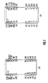
- Figs. 1(A) and Fig. 1(B) show pin arrangements of a semiconductor memory device which makes a shared use of a pellet, and makes it possible to go to a one-bit configuration (Fig. 1(A)) and a multi-bit configuration (Fig. 1(B)) by switching the connection between external terminals and lead frames.
- address input signals A0 to A10 applied to pin 9 to pin 12, pin 14 and pin 18, pin 22 and pin 5 are made effective in time series, and made to become a column address and a row address by a column address strobe signal CAS that is applied to 24 and a row address signal RAS applied to pin 3, respectively.
- a write amplifier enable signal WE applied to pin 2 designates the difference between the write operation to the memory cell array and the read operation from the memory cell array. In the case of the write operation, a data input signal D IN applied to the pin 1 is written to the memory cell array, while in the case of the read operation, a data output signal D OUT is read out from the memory cell array at the pin 25.
- the device operates as a semiconductor memory device of one-bit configuration with 1022 addresses x 1 bit.
- Fig. 1(B) the pin arrangement for the upper half part of the figure differs from that of Fig. 1(A). Namely, since the pin 22 in Fig. 1(A) is replaced in Fig. 1(B) by a pin 22B of output enable signal OE , the address input signal for this case becomes 10 bits of A0 to A9. However, each of the terminals 1 and 25 for the data input signal D IN and the data output signal D OUT , respectively, in Fig. 1(A) is used in Fig. 1(B) commonly for the input and the output, and by providing terminals 1B, 2B, 24B and 25B for altogether four data input and output signals I/O1 to I/O4, simultaneous input or output of 4 bits becomes possible. The difference between the write operation and the read operation is designated by the output enable signal OE (pin 22A). As a result, the device operates as a semiconductor memory device of multi-bit configuration with 1020 addresses x 4 bits.
- the one-bit configuration and the multi-bit configuration in the above can be affected by a simple switching of the lead frame connections for the pins of the semiconductor memory device without involving any change in the internal configuration of the device.
- the data input terminals for X4 configuration correspond to the pins 1B, 2B, 24B and 25B for the data input and output signals of the semiconductor memory device of the four-bit configuration shown in Fig. 1(B). Since the write operation will be described in what follows, these terminals will function as the data input terminals.
- a signal data applied to the data input terminals for X4 configuration of the semiconductor memory device at the time when a control signal 0 ⁇ 1 went from the level “1" to the level “0” is latched as a write mask data.
- a signal data applied to the data input terminals for X4 configuration of the semiconductor memory device at the time when a control signal 0 ⁇ 2 goes from "1" to "0” is latched as a write data for writing. If a write mask data which is input to the same input terminal is "1", the write data will be written to the memory cell array while if it is "0", the write data will not be written to the memory cell array.
- the write mask function operates for every bit of a data so that it will be meaningless unless the semiconductor memory device is of the multi-bit input and output configuration.
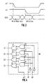
- Fig. 3 shows a block diagram for the parts that are related only to the write operation of the memory.
- a memory cell array S1 is divided into four sections in order to permit a simultaneous operation at the time of the X4 configuration.
- the row decoders S2 and the column decoders S3 decode the input address signals for the one-bit configuration of the four-bit configuration in response to the row address strobe signals RAS and the column address strobe signal CAS , respectively, to drive the row address lines and the column address lines of the memory cell array S1.
- the write amplifiers 101 to 104 are for writing data to the memory cells that are selected as in the above, the reason for having four amplifiers being, to be able to handle the case of the four-bit configuration.
- a control signal 0 ⁇ 3 is "0" that is, when the device is in the one-bit configuration
- a selector 70 selects either one of the four write data lines WD1 to WD4 using the input address signals A1 and A2, and connects the selected line to a write data line WD5.
- the control signal 0 ⁇ 3 is usually generated by a known programmable circuit means such as a fuse.
- the control signal 0 ⁇ 3 is "1" that is, when the device is in the four-bit configuration, the device is operated so as to connect the write data line WD5 to none of the write data lines WD1 to WD5.
- a write data input circuit 60 supplies a write data input from a data input terminal 50 for X1 (namely, one-bit) configuration to the write data line WD5 in response to the control signal 0 ⁇ 2 for data fetching.
- the four write data input circuits 31 to 34 supply the write data that are input through data input terminals 201 to 204 for the X4 configuration to write data lines WD1 to WD4, respectively, in response to the control signal 0 ⁇ 2.
- the four write mask data input circuits 41 and 44 supply write mask data that are input through data input terminals 201 to 204 for the X4 configuration to write mask data lines MD1 to MD4, respectively in response to the write mask data fetching control signal 0 ⁇ 1.
- a write mask decoder 80 sets only one line among four write amplifier enable signal lines E1 to E4 to "1” by decoding the input address signals A1 to A2 when the control signal 0 ⁇ 3 is "0", and sets all of the write amplifier enable signal lines E1 to E4 to "1" when the control signal 0 ⁇ 3 is "1".
- Fig. 4 is shown the logic gate configuration of the write mask decoder 80.
- the control signal 0 ⁇ 3 is "1"
- all of the four two-input OR gates Gl output "1" so that all of the four write amplifier enable signal lines E1 to E4 go to "1".
- the control signal 0 ⁇ 3 is "0”
- the outputs of the four of the two-input AND gates G2 are output as they are to the write amplifier enable signal lines E1 to E4.
- the four of the two-gate AND gates G2 and the two inverters G3 decode the input address signals A1 and A2, and output "1" from only one of the two-input AND gates G2 and "0” from the remaining two-input AND gates G2.
- the control signal 0 ⁇ 3 goes to "0" at the time of one-bit configuration, either one of the write amplifier enable signal lines E1 to E4 es set to "1" by the write mask decoder 80 in response to the input address signals A1 and A2, and only the write amplifier 101, for example, connected to that particular line is activated. Then, the write data line WD1 connected to the activated write amplifier 101 and the write data line WD5 are connected by the selector 70, and the data in the write data line WD5 is written to the memory cell array by the activated write amplifier 101.
- the control signal goes to "1"
- all of the write amplifier enable signal lines E1 to E4 go to "1" whereby activating all of the write amplifiers 101 to 104.
- the write mask data lines MD1 to MD4 are "1”
- the data in the write data lines WD1 to WD4 that are in the paired relation by being connected to the write amplifiers 101 to 104 with the same number of bits are written to the memory cell arrays.
- the write mask data lines MD1 to MD4 are "0" the data in the write data lines WD1 to WD4 are not written to the memory cell, whereby effecting the write masking.
- Fig. 5 shows the circuit layout on the common pellet for the 4 megabit DRAM in Fig. 1.
- the figure sketches the outline of the actual product, with the size ratio of the long and short sides being substantially equal to the true value of the actual product. (Note that terminals that are not needed for the description are dropped from the figure.)
- 16 write amplifiers 110 are uniformly disposed along both sides of the memory cell arrays S110 that consist of 16 parts in all.
- the selector 70 selects one of 16 write amplifiers 110 in the X1 input configuration and selects four of the 16 write amplifiers simultaneously in the X4 input configuration.
- a data input terminal 1a for the X1 configuration In the write-hand end section along the short side of the pellet there are compactly arranged a data input terminal 1a for the X1 configuration, data input terminals 1b, 2b, 24b and 25b for the X4 configuration, a write data input circuit 60, integrated units of a data input circuit 30 and a write mask data input circuit 40, a selector 70 and a mask decoder 90. Accordingly, it will be easily understood that the separation between the write mask data input circuit 40 and the write mask decoder 90 is smaller than the separation between the write mask data input circuit 40 and the write amplifier 110.
- the write mask data lines MD1 to MD4 that connect the write mask data input circuit 40 and the write amplifiers 110 have to be run over fairly long distances which requires an accordingly large wiring area. This becomes, therefor, a big obstacle to the miniaturization effort for the pellet.
- the write data lines WD1 to WD4 and the write amplifier enable signal lines E1 to E4 in addition to the write mask data lines MD1 to MD4 enter the write amplifiers 110.
- these lines run adjacent with each other for a relatively long distance so that the parasitic capacitance is increased, and consequently the operational performance of the pellet will be deteriorated.
- Figure 6 is a block diagram showing the semiconductor memory device according to a first embodiment of the present invention.
- the components identical to those in the prior art device are assigned the identical symbols to avoid the duplication of the explanation, with only characteristic features being described.
- the pin arrangement, the write mask function and the circuit layout on the pellet are as shown in Fig. 1, Fig. 2 and Fig. 5, respectively.
- the write mask data lines MD1 to MD4 from the write mask data input circuits 41 to 44 are connected to the write mask decoder 90, and the write mask data on the lines MD1 to MD4 are input to write amplifiers 111 to 114 by the write amplifier enable signal lines E1 to E4 leading from the write mask decoder 90 to the write amplifiers 111 to 114.
- the write mask data lines MD1 to MD4 and the write amplifier enable signal lines E1 to E4 are serially connected via the write mask decoder 90.
- the write mask decoder 90 selects one line among the write amplifier enable signal lines E1 to E4 by decoding the input address signals A1 and A2 and outputs "1" at the time of the one-bit configuration, and outputs the write mask data on the signal lines MD1 to MD4 to the write amplifier enable signal lines E1 to E4 for all times regardless of the values of the input address signals A1 and A2 at the time of four-bit configuration.
- the write amplifiers 111 to 114 are controlled by the write amplifier enable signal lines E1 to E4 alone. It is to be noted that this control operates under the same logic as that of the direct control by the write mask data lines MD1 to MD4 and the write amplifier enable signal lines E1 to E4 in Fig. 3.
- the control signal 0 ⁇ 3 may be generated by a known programmable circuit means such as disclosed in U.S. Patent Specification 4,571,707 issued to Watanabe.
- the write amplifiers 111 ⁇ 114 the amplifier such as disclosed in U.S. Patent Specification 4,669,064 issued to Ishimoto may be utilized.
- Fig. 7 shows the logic gate configuration of the write mask data decoder 90.
- G4 is a three-input AND gate, and the remaining components are the same as shown in Fig. 4.
- the decoder 90 outputs the values of the write mask data lines MD1 to MD4 to the write amplifier enable signal lines E1 to E4 when the control signal 0 ⁇ 3 is "1", and outputs "1" only to one line among E1 to E4 and "0" to the remainder depending upon the values of the input address signals A1 and A2 when the control signal 0 ⁇ 3 is "0".
- the control signal 0 ⁇ 3 becomes "0"
- either one of the four write amplifier enable signal lines E1 to E4 is set to "1" by the input address signals A1 and A2, and only the connected one 111, for example, of the write amplifiers is activated.
- the write data line WD5 is connected by the selector 70 to the write data line WD1 that is connected to the write amplifier 111, and the data of the write data line WD5 is written to the memory cell array.
- Fig. 8 is a block diagram for the semiconductor memory device in accordance with a second embodiment of the present invention. It is to be noted that the components identical to those of the prior art device and the first embodiment are assigned the identical symbols to avoid a duplicated explanation, and the characteristic features alone of the present embodiment will be described.
- a write mask decoder 91 is controlled by the control signal 0 ⁇ 3 and decodes the input address signals A1 and A2, but its outputs are introduced to the corresponding newly provided selectors 121 to 124 through the signal lines ES1 to ES4.
- Each of the selectors 121 to 124 selects either one of the write mask data lines MD1 and the like and the signal lines ES1 and the like by the control of the control signal 0 ⁇ 3, and inputs the signal to the corresponding one of the write amplifiers 111 to 114 by connecting the selected line to the corresponding write amplifier enable signal lines E1 and the like. Since the selectors 121 to 124 can be arranged at substantially the same positions of the write data input circuit 30 and the write mask data input circuit 40 on the circuit layout in Fig. 5, the write mask data lines MD1 to MD4 and the signal lines ES1 to ES4 in Fig. 8 can be made relatively short.
- Fig. 9 is shown the logic gate configuration of the write mask decoder 91.
- the decoder 91 either one of the signal lines ES1 to ES4 is set to “1" by the input address signals A1 and A2 when the control signal 0 ⁇ 3 is “0", and all of the signal lines are set to "0" when the control signal 0 ⁇ 3 is "1".
- Fig. 10 is shown the logic gate configuration of the selectors 121 to 124.
- the subscript i on the symbols takes on the values 1 to 4.
- the write amplifier enable lines and the write mask data lines are serially connected so that the number of the input signal lines for the write amplifiers can be reduced to two-thirds. That is, in the past, the write data lines, the write amplifier enable signal lines and the write mask data lines were connected to the write amplifiers, but in the present invention it is only needed to connect the write data lines and the write amplifier enable signal lines. Moreover, each of these input signal lines are required for the same number as the number of the write amplifiers to that the absolute number that can be reduced can be made to be equal to that of the write amplifiers.
- Each of the above-mentioned input signal lines becomes relatively long due to the circuit layout of the semiconductor memory device so that the line arrangement area can be reduced by the decrease in their number, which brings about a significant effect in the attempt to miniaturize the semiconductor memory device.
- the reduction in the parasitic capacitance will enhance the operational performance of the device.
- the wiring area can be reduced from 3840 ⁇ m2 to 3584 ⁇ m2 and the parasitic capacitance can be reduced by 16 pF.
Abstract
Description
- The present invention relates to a semiconductor integrated circuit (IC) memory (referred to as "semiconductor memory device" hereinafter), and more particularly to a semiconductor memory device which may be used by switching in the one-bit input and output mode as well as in the multi-bit input and output mode with the shared use of a same pellet, and enables memory write masking.
- The majority of the semiconductor memory devices in the early days had the one-bit input and output mode configuration which input or output only one-bit data for the main purpose of suppressing the increase in the number of IC pins. However, the mass storage has been accelerated as the application field of the semiconductor memory devices has expanded with the improvement in the level of integration, and devices have been developed with multi-bit input and output mode configuration which simultaneously inputs or outputs data with a plurality of bits. In such a semiconductor memory device the same address terminal is multiply used in time series for a row address signal and for a column address signal, and the same terminal is used for data input and for data output by switching between them.
- Now, under the semiconductor development race which has become increasingly vehement in recent years, it is becoming general to adopt a technique in which there is arranged a circuit necessary for both one-bit input and output mode configuration (abbreviated as one-bit configuration hereinafter) and multi-bit input and output mode configuration (abbreviated as multi-bit configuration hereinafter), and these configurations are changed by switching between them with a bonding or a mask. It is to be noted that even for a semiconductor memory device to be used in one-bit configuration such a technique is effective at a time of testing in reducing the test time, which has been recognized as a problem that accompanies the advancement in the level of integration, by giving the device the multi-bit configuration. In a semiconductor memory device of this technique the multi-bit configuration is dealt with by providing write amplifiers in a number at least equal to that of the bits that can be written simultaneously, and a selector that selects one write amplifier based on the address signals is provided to handle the case of one-bit configuration.
- In the semiconductor memory devices of the multi-bit configuration such as in the case used as a RAM for image in CRT or the like, there arise many instances in which there is required the memory write masking function which can invalidate the information writing to, that is, which can write mass every one of the bits. Conventionally, memory write masking is executed by providing write mask data input circuits corresponding to the respective write amplifiers that input write mask data from data input terminals and supply them to write amplifiers at the time of multi-bit configuration, and a write mask decoder which decodes the address signals that are identical to the address signals that are supplied to the selector, and supplies a write amplifier enable signal to one of the write amplifiers only at the time of one-bit configuration. In other words, write masking is executed by inputting write mask data that are not subjected to address selection within the semiconductor memory device and a write amplifier enable signal that is subjected to address selection within the semiconductor memory device, to a write amplifiers.
- Accordingly, there are required a large number of control signal lines for write amplifiers, and from the layout design for the semiconductor memory devices the write amplifiers are arranged substantially removed from the write mask data input circuits and the write mask decoder. Because of this, the wiring area becomes large which has been a serious obstacle to the miniaturization effort for the semiconductor memory device. Moreover, an increase in the wiring area leads to an increase in the parasitic capacitance which also gives rise to a problem in conjunction with the effort for enhancing the operational performance.
- Accordingly, it is a first object of the present invention to provide a semiconductor memory device with reduced area for the wiring.
- It is a second object of the present invention to provide a semiconductor memory device which can realize the miniaturization.
- Furthermore, it is a third object of the present invention to provide a semiconductor memory device which can realize an enhancement of the operational performance.
- The present invention relates to a semiconductor memory device which shares a pellet for its use by switching for the one-bit input and output mode and the multi-bit input and output mode, and enables the memory write masking. In the present invention, each of a plurality of write amplifiers which execute data write to a memory cell array is connected to a write data line that transmits a write data and a write amplifier enable signal line that controls the activation of the write amplifier to receive inputs from these two lines. In addition, there is provided means for inputting a write mask data specifying a write mask for every bit to a write amplifier via a write amplifier enable signal line for the case of multi-bit configuration.
- In the semiconductor memory device of the present invention, it is preferable to be equipped with means for receiving a control signal that specifies the one-bit configuration and the multi-bit configuration, and a selection circuit which, in response to the control signal, selects one write amplifier enable signal line that is designated by the address signal for the case of one-bit configuration, and outputs on the write amplifier enable signal lines a write mask data that consists of binary information with the same number as the write amplifier enable signal lines that are externally input, for the case of multi-bit configuration.
- Moreover, for the semiconductor memory device of the present invention it is preferable to provide a write mask decoder which activates one of the write amplifier enable signal lines by decoding the address signals for the one-bit configuration, and outputs a write mask data input externally, as it is, on the write amplifier enable signal lines for the multi-bit configuration.
- Furthermore, for the semiconductor memory device of the present invention it is preferable to provide a write mask decoder which decodes the address signals to activate one of the outputs only when it is in the one-bit configuration, and a selector which selects an activated output and sends it out to a write amplifier enable signal line for the one-bit configuration, and sends out a write mask data externally input to the write amplifier enable signal lines for the multi-bit configuration.
- In accordance with the present invention the number of signal lines for controlling the write amplifiers can be reduced. Accordingly, the area to be used for the wiring can be reduced, and the miniaturization and the enhancement of the operational performance of the semiconductor memory device can be achieved.
- The above-mentioned and other objects, features and advantages of this invention will become more apparent from the following detailed description of the invention taken in conjunction with the accompanying drawings, wherein:
- Fig. 1 shows the pin arrangement of a 4-megabit dynamic random access memory (DRAM);
- Fig. 2 shows a voltage waveform diagram for explaining the write mask function;
- Fig. 3 shows a block diagram of the prior art;
- Fig. 4 shows a logic gate diagram of the write mask decoder in Fig. 3;
- Fig. 5 shows the layout of a 4-megabit DRAM;
- Fig. 6 shows a block diagram for the semiconductor memory device in accordance with a first embodiment of the present invention;
- Fig. 7 shows a logic gate diagram of the write mask decoder in Fig. 6;
- Fig. 8 shows a block diagram for the semiconductor memory device in accordance of a second embodiment of the present invention;
- Fig. 9 shows a logic gate diagram of the write mask decoder in Fig. 8; and
- Fig. 10 shows a logic gate diagram of the selector in Fig. 8.
- Prior to the description of the embodiments in accordance with the present invention, a general description of the switching of the connection between the one-bit configuration and the multi-bit configuration and the write mask function of the semiconductor memory device, and a description of the prior art memory write mask system are in order.
- Figs. 1(A) and Fig. 1(B) show pin arrangements of a semiconductor memory device which makes a shared use of a pellet, and makes it possible to go to a one-bit configuration (Fig. 1(A)) and a multi-bit configuration (Fig. 1(B)) by switching the connection between external terminals and lead frames.
- In Fig. 1(A), address input signals A₀ to A₁₀ applied to
pin 9 topin 12, pin 14 andpin 18,pin 22 andpin 5 are made effective in time series, and made to become a column address and a row address by a column address strobe signalCAS that is applied to 24 and a row address signalRAS applied topin 3, respectively. A write amplifier enable signalWE applied topin 2 designates the difference between the write operation to the memory cell array and the read operation from the memory cell array. In the case of the write operation, a data input signal DIN applied to thepin 1 is written to the memory cell array, while in the case of the read operation, a data output signal DOUT is read out from the memory cell array at the pin 25. As a result, the device operates as a semiconductor memory device of one-bit configuration with 10²² addresses x 1 bit. - In Fig. 1(B), the pin arrangement for the upper half part of the figure differs from that of Fig. 1(A). Namely, since the
pin 22 in Fig. 1(A) is replaced in Fig. 1(B) by apin 22B of output enable signalOE , the address input signal for this case becomes 10 bits of A₀ to A₉. However, each of theterminals 1 and 25 for the data input signal DIN and the data output signal DOUT, respectively, in Fig. 1(A) is used in Fig. 1(B) commonly for the input and the output, and by providingterminals 1B, 2B, 24B and 25B for altogether four data input and output signals I/O₁ to I/O₄, simultaneous input or output of 4 bits becomes possible. The difference between the write operation and the read operation is designated by the output enable signalOE (pin 22A). As a result, the device operates as a semiconductor memory device of multi-bit configuration with 10²⁰ addresses x 4 bits. - The one-bit configuration and the multi-bit configuration in the above can be affected by a simple switching of the lead frame connections for the pins of the semiconductor memory device without involving any change in the internal configuration of the device.
- Next, referring to Fig. 2, the function of the write mask will be described.
- It is to be noted that what is called the data input terminals for X4 configuration correspond to the
pins 1B, 2B, 24B and 25B for the data input and output signals of the semiconductor memory device of the four-bit configuration shown in Fig. 1(B). Since the write operation will be described in what follows, these terminals will function as the data input terminals. - First, a signal data applied to the data input terminals for X4 configuration of the semiconductor memory device at the time when a control signal 0̸1 went from the level "1" to the level "0" is latched as a write mask data. In addition, a signal data applied to the data input terminals for X4 configuration of the semiconductor memory device at the time when a control signal 0̸2 goes from "1" to "0" is latched as a write data for writing. If a write mask data which is input to the same input terminal is "1", the write data will be written to the memory cell array while if it is "0", the write data will not be written to the memory cell array. The write mask function operates for every bit of a data so that it will be meaningless unless the semiconductor memory device is of the multi-bit input and output configuration.
- Referring to Fig. 3, the prior art memory write mask system in a semiconductor memory device which makes the multi-bit configuration operative and has the write mask function will be described.
- Fig. 3 shows a block diagram for the parts that are related only to the write operation of the memory.
- A memory cell array S1 is divided into four sections in order to permit a simultaneous operation at the time of the X4 configuration. The row decoders S2 and the column decoders S3 decode the input address signals for the one-bit configuration of the four-bit configuration in response to the row address strobe signals
RAS and the column address strobe signalCAS , respectively, to drive the row address lines and the column address lines of the memory cell array S1. - The
write amplifiers 101 to 104 are for writing data to the memory cells that are selected as in the above, the reason for having four amplifiers being, to be able to handle the case of the four-bit configuration. When a control signal 0̸3 is "0", that is, when the device is in the one-bit configuration, aselector 70 selects either one of the four write data lines WD1 to WD4 using the input address signals A₁ and A₂, and connects the selected line to a write data line WD5. The control signal 0̸3 is usually generated by a known programmable circuit means such as a fuse. Further, when the control signal 0̸3 is "1", that is, when the device is in the four-bit configuration, the device is operated so as to connect the write data line WD5 to none of the write data lines WD1 to WD5. - A write
data input circuit 60 supplies a write data input from adata input terminal 50 for X1 (namely, one-bit) configuration to the write data line WD5 in response to the control signal 0̸2 for data fetching. The four writedata input circuits 31 to 34 supply the write data that are input throughdata input terminals 201 to 204 for the X4 configuration to write data lines WD1 to WD4, respectively, in response to the control signal 0̸2. - The four write mask
data input circuits data input terminals 201 to 204 for the X4 configuration to write mask data lines MD1 to MD4, respectively in response to the write mask data fetching control signal 0̸1. Awrite mask decoder 80 sets only one line among four write amplifier enable signal lines E1 to E4 to "1" by decoding the input address signals A₁ to A₂ when the control signal 0̸3 is "0", and sets all of the write amplifier enable signal lines E1 to E4 to "1" when the control signal 0̸3 is "1". - In Fig. 4 is shown the logic gate configuration of the
write mask decoder 80. When the control signal 0̸3 is "1", all of the four two-input OR gates Gl output "1" so that all of the four write amplifier enable signal lines E1 to E4 go to "1". On the other hand, when the control signal 0̸3 is "0", the outputs of the four of the two-input AND gates G2 are output as they are to the write amplifier enable signal lines E1 to E4. The four of the two-gate AND gates G2 and the two inverters G3 decode the input address signals A₁ and A₂, and output "1" from only one of the two-input AND gates G2 and "0" from the remaining two-input AND gates G2. - Thus, referring to Fig. 3, the control signal 0̸3 goes to "0" at the time of one-bit configuration, either one of the write amplifier enable signal lines E1 to E4 es set to "1" by the
write mask decoder 80 in response to the input address signals A₁ and A₂, and only thewrite amplifier 101, for example, connected to that particular line is activated. Then, the write data line WD1 connected to the activatedwrite amplifier 101 and the write data line WD5 are connected by theselector 70, and the data in the write data line WD5 is written to the memory cell array by the activatedwrite amplifier 101. - Further, at the time of the four-bit configuration the control signal goes to "1", all of the write amplifier enable signal lines E1 to E4 go to "1", whereby activating all of the
write amplifiers 101 to 104. If then the write mask data lines MD1 to MD4 are "1", the data in the write data lines WD1 to WD4 that are in the paired relation by being connected to thewrite amplifiers 101 to 104 with the same number of bits are written to the memory cell arrays. On the other hand, if the write mask data lines MD1 to MD4 are "0", the data in the write data lines WD1 to WD4 are not written to the memory cell, whereby effecting the write masking. - Fig. 5 shows the circuit layout on the common pellet for the 4 megabit DRAM in Fig. 1. The figure sketches the outline of the actual product, with the size ratio of the long and short sides being substantially equal to the true value of the actual product. (Note that terminals that are not needed for the description are dropped from the figure.) In this example 16
write amplifiers 110 are uniformly disposed along both sides of the memory cell arrays S110 that consist of 16 parts in all. In this arrangement, theselector 70 selects one of 16write amplifiers 110 in the X1 input configuration and selects four of the 16 write amplifiers simultaneously in the X4 input configuration. In the write-hand end section along the short side of the pellet there are compactly arranged adata input terminal 1a for the X1 configuration,data input terminals data input circuit 60, integrated units of a data input circuit 30 and a write mask data input circuit 40, aselector 70 and amask decoder 90. Accordingly, it will be easily understood that the separation between the write mask data input circuit 40 and thewrite mask decoder 90 is smaller than the separation between the write mask data input circuit 40 and thewrite amplifier 110. - If it is assumed that the prior art memory write device in Fig. 3 is applied to the memory in Fig. 5, the write mask data lines MD1 to MD4 that connect the write mask data input circuit 40 and the
write amplifiers 110 have to be run over fairly long distances which requires an accordingly large wiring area. This becomes, therefor, a big obstacle to the miniaturization effort for the pellet. Further, in this case, the write data lines WD1 to WD4 and the write amplifier enable signal lines E1 to E4 in addition to the write mask data lines MD1 to MD4 enter thewrite amplifiers 110. Moreover, these lines run adjacent with each other for a relatively long distance so that the parasitic capacitance is increased, and consequently the operational performance of the pellet will be deteriorated. - Next, the embodiments of the present invention will be described.
- Figure 6 is a block diagram showing the semiconductor memory device according to a first embodiment of the present invention. In the description, the components identical to those in the prior art device are assigned the identical symbols to avoid the duplication of the explanation, with only characteristic features being described.
- Further, when the present semiconductor memory device is applied to a 4 megabit memory, the pin arrangement, the write mask function and the circuit layout on the pellet are as shown in Fig. 1, Fig. 2 and Fig. 5, respectively.
- In the present invention, the write mask data lines MD1 to MD4 from the write mask
data input circuits 41 to 44 are connected to thewrite mask decoder 90, and the write mask data on the lines MD1 to MD4 are input to writeamplifiers 111 to 114 by the write amplifier enable signal lines E1 to E4 leading from thewrite mask decoder 90 to thewrite amplifiers 111 to 114. Namely, the write mask data lines MD1 to MD4 and the write amplifier enable signal lines E1 to E4 are serially connected via thewrite mask decoder 90. - The
write mask decoder 90 selects one line among the write amplifier enable signal lines E1 to E4 by decoding the input address signals A₁ and A₂ and outputs "1" at the time of the one-bit configuration, and outputs the write mask data on the signal lines MD1 to MD4 to the write amplifier enable signal lines E1 to E4 for all times regardless of the values of the input address signals A₁ and A₂ at the time of four-bit configuration. - As a result, the
write amplifiers 111 to 114 are controlled by the write amplifier enable signal lines E1 to E4 alone. It is to be noted that this control operates under the same logic as that of the direct control by the write mask data lines MD1 to MD4 and the write amplifier enable signal lines E1 to E4 in Fig. 3. In this embodiment, the control signal 0̸3 may be generated by a known programmable circuit means such as disclosed in U.S. Patent Specification 4,571,707 issued to Watanabe. As thewrite amplifiers 111 ∼ 114, the amplifier such as disclosed in U.S. Patent Specification 4,669,064 issued to Ishimoto may be utilized. - Fig. 7 shows the logic gate configuration of the write
mask data decoder 90. In the figure, G4 is a three-input AND gate, and the remaining components are the same as shown in Fig. 4. As may be clear from the figure, thedecoder 90 outputs the values of the write mask data lines MD1 to MD4 to the write amplifier enable signal lines E1 to E4 when the control signal 0̸3 is "1", and outputs "1" only to one line among E1 to E4 and "0" to the remainder depending upon the values of the input address signals A₁ and A₂ when the control signal 0̸3 is "0". - Namely, in Fig. 6, at the time of the four-bit configuration the control signal 0̸3 becomes "1", and if the write mask data lines MD1 to MD4 are "1", the corresponding write amplifier enable signal lines E1 to E4 also become "1" via the
write mask decoder 90, and the data of the write data lines WD1 to WD4 that are paired with the data lines MD1 to MD4 are written to the memory cell arrays S1 by the activatedwrite amplifiers 111 to 114. - Further, even when the control signal 0̸3 is "1", if the write mask data lines MD1 to MD4 are "0", the corresponding write amplifier enable signal lines E1 to E4 also become "0" via the
write mask decoder 90, and the data of the write data lines WD1 to WD4 are not write to the memory cell arrays whereby effecting the write masking. - On the other hand, at the time of the one-bit configuration the control signal 0̸3 becomes "0", either one of the four write amplifier enable signal lines E1 to E4 is set to "1" by the input address signals A₁ and A₂, and only the connected one 111, for example, of the write amplifiers is activated. Then, the write data line WD5 is connected by the
selector 70 to the write data line WD1 that is connected to thewrite amplifier 111, and the data of the write data line WD5 is written to the memory cell array. - Fig. 8 is a block diagram for the semiconductor memory device in accordance with a second embodiment of the present invention. It is to be noted that the components identical to those of the prior art device and the first embodiment are assigned the identical symbols to avoid a duplicated explanation, and the characteristic features alone of the present embodiment will be described.
- In the present embodiment, four
selectors data input circuits 41 to 44 are connected to theselectors 121 to 124, respectively. Analogous to the prior artwrite mask decoder 80 shown in Fig. 3, awrite mask decoder 91 is controlled by the control signal 0̸3 and decodes the input address signals A₁ and A₂, but its outputs are introduced to the corresponding newly providedselectors 121 to 124 through the signal lines ES1 to ES4. - Each of the
selectors 121 to 124 selects either one of the write mask data lines MD1 and the like and the signal lines ES1 and the like by the control of the control signal 0̸3, and inputs the signal to the corresponding one of thewrite amplifiers 111 to 114 by connecting the selected line to the corresponding write amplifier enable signal lines E1 and the like. Since theselectors 121 to 124 can be arranged at substantially the same positions of the write data input circuit 30 and the write mask data input circuit 40 on the circuit layout in Fig. 5, the write mask data lines MD1 to MD4 and the signal lines ES1 to ES4 in Fig. 8 can be made relatively short. - Although the invention has been described with reference to specified embodiments, this description is not meant to be construed in a limiting sense. Various modifications of the disclosed embodiments will become apparent to persons skilled in the art upon reference to the description of the invention. It is therefore contemplated that the appended claims will cover any modifications or embodiments that fall within the true scope of the invention.
- In Fig. 9 is shown the logic gate configuration of the
write mask decoder 91. In thedecoder 91 either one of the signal lines ES1 to ES4 is set to "1" by the input address signals A₁ and A₂ when the control signal 0̸3 is "0", and all of the signal lines are set to "0" when the control signal 0̸3 is "1". - In Fig. 10 is shown the logic gate configuration of the
selectors 121 to 124. In the figure the subscript i on the symbols takes on thevalues 1 to 4. With these selectors, when the control signal 0̸3 is "0", the values of the signal lines ES1 to ES4 are output as they are to the write amplifier enable signal lines E1 to E4, and when the control signal 0̸3 is "1", the values of the write mask data lines MD1 to MD4 are output as they are to the write amplifier enable signal lines E1 to E4. - With the device as shown in Fig. 8 an operation similar to the embodiment shown in Fig. 6 can be obtained.
- In the present embodiment there can be obtained an advantage that the number of wirings can be reduced without requiring to lead the write mask data lines MD1 to MD4 to the
write mask decoder 91. - In the present embodiment the write amplifier enable lines and the write mask data lines are serially connected so that the number of the input signal lines for the write amplifiers can be reduced to two-thirds. That is, in the past, the write data lines, the write amplifier enable signal lines and the write mask data lines were connected to the write amplifiers, but in the present invention it is only needed to connect the write data lines and the write amplifier enable signal lines. Moreover, each of these input signal lines are required for the same number as the number of the write amplifiers to that the absolute number that can be reduced can be made to be equal to that of the write amplifiers.
- Each of the above-mentioned input signal lines becomes relatively long due to the circuit layout of the semiconductor memory device so that the line arrangement area can be reduced by the decrease in their number, which brings about a significant effect in the attempt to miniaturize the semiconductor memory device. Moreover, the reduction in the parasitic capacitance will enhance the operational performance of the device. For example, when the present invention is applied to a semiconductor memory device with chip size of 16 mm x 6 mm and a wiring pitch of 4 µm, the wiring area can be reduced from 3840 µm² to 3584 µm² and the parasitic capacitance can be reduced by 16 pF.
Claims (9)
a memory cell array;
a write amplifier for operatively performing a data write operation to said memory cell array;
a write data line connected to said write amplifier for supplying a write data;
a write amplifier enable signal line connected to said write amplifier for controlling the activation of said write amplifier;
means for receiving from the outside a write mask data for designating write mask for each bit at the time of said multi-bit input and output mode configuration; and
means connected to said receiving means and said write amplifier enable signal line for supplying a write mask data received by said receiving means from the outside to said write amplifier enable signal line at the time of said multi-bit input and output mode configuration.
connecting, to each of the write amplifiers for executing data write to a memory cell array, a write data line for transmitting a write data and a write amplifier enable signal line for controlling the activation of said write amplifier; and
inputting a write mask data for designating a write mask for every bit to said write amplifiers by means of said write amplifier enable signal lines at the time of multi-bit input and output mode configuration.
a selector which respectively sends said output at the time of one-bit input and output mode configuration, and a write mask data input from said input terminal at the time of multi-bit input and output mode configuration, as they are, to said write amplifier enable signal lines.
Applications Claiming Priority (2)
| Application Number | Priority Date | Filing Date | Title |
|---|---|---|---|
| JP45824/89 | 1989-02-27 | ||
| JP4582489 | 1989-02-27 |
Publications (3)
| Publication Number | Publication Date |
|---|---|
| EP0385389A2 true EP0385389A2 (en) | 1990-09-05 |
| EP0385389A3 EP0385389A3 (en) | 1992-09-30 |
| EP0385389B1 EP0385389B1 (en) | 1995-06-28 |
Family
ID=12729996
Family Applications (1)
| Application Number | Title | Priority Date | Filing Date |
|---|---|---|---|
| EP90103784A Expired - Lifetime EP0385389B1 (en) | 1989-02-27 | 1990-02-27 | Semiconductor integrated circuit memory enabling memory write masking |
Country Status (3)
| Country | Link |
|---|---|
| US (1) | US5148396A (en) |
| EP (1) | EP0385389B1 (en) |
| DE (1) | DE69020384T2 (en) |
Cited By (7)
| Publication number | Priority date | Publication date | Assignee | Title |
|---|---|---|---|---|
| DE4236455A1 (en) * | 1992-05-25 | 1993-12-02 | Mitsubishi Electric Corp | Semiconductor memory device with a bitwise write function in page mode |
| EP0573800A1 (en) * | 1992-06-09 | 1993-12-15 | Siemens Aktiengesellschaft | Integrated semi-conductor memory device |
| GB2271449A (en) * | 1992-09-29 | 1994-04-13 | Ricoh Kk | Dram and controller |
| US5329493A (en) * | 1992-06-09 | 1994-07-12 | Siemens Aktiengesellschaft | Integrated semiconductor memory array and method for operating the same |
| WO1994029871A1 (en) * | 1993-06-14 | 1994-12-22 | Rambus, Inc. | Method and apparatus for writing to memory components |
| EP0655741A2 (en) * | 1993-11-29 | 1995-05-31 | Kabushiki Kaisha Toshiba | Memory device and serial-parallel data transform circuit |
| EP0895162A2 (en) * | 1992-01-22 | 1999-02-03 | Enhanced Memory Systems, Inc. | Enhanced dram with embedded registers |
Families Citing this family (15)
| Publication number | Priority date | Publication date | Assignee | Title |
|---|---|---|---|---|
| GB9116493D0 (en) * | 1991-07-30 | 1991-09-11 | Inmos Ltd | Read and write circuitry for a memory |
| JP2743653B2 (en) * | 1991-09-20 | 1998-04-22 | 富士通株式会社 | Semiconductor storage device |
| US5539696A (en) * | 1994-01-31 | 1996-07-23 | Patel; Vipul C. | Method and apparatus for writing data in a synchronous memory having column independent sections and a method and apparatus for performing write mask operations |
| US5526320A (en) | 1994-12-23 | 1996-06-11 | Micron Technology Inc. | Burst EDO memory device |
| US5778428A (en) * | 1995-12-22 | 1998-07-07 | International Business Machines Corporation | Programmable high performance mode for multi-way associative cache/memory designs |
| US6167486A (en) | 1996-11-18 | 2000-12-26 | Nec Electronics, Inc. | Parallel access virtual channel memory system with cacheable channels |
| WO1999019875A2 (en) * | 1997-10-10 | 1999-04-22 | Rambus Incorporated | Apparatus and method for pipelined memory operations |
| JP4007673B2 (en) * | 1998-03-31 | 2007-11-14 | 富士通株式会社 | Memory device |
| US6330636B1 (en) | 1999-01-29 | 2001-12-11 | Enhanced Memory Systems, Inc. | Double data rate synchronous dynamic random access memory device incorporating a static RAM cache per memory bank |
| JP2001084791A (en) * | 1999-07-12 | 2001-03-30 | Mitsubishi Electric Corp | Semiconductor memory |
| US6708254B2 (en) | 1999-11-10 | 2004-03-16 | Nec Electronics America, Inc. | Parallel access virtual channel memory system |
| DE10002130A1 (en) * | 2000-01-19 | 2001-08-02 | Infineon Technologies Ag | Method and device for alternately operating a read-write memory in the one-memory operating mode and in the entangled multi-memory operating mode |
| US6529425B2 (en) | 2000-11-13 | 2003-03-04 | Kabushiki Kaisha Toshiba | Write prohibiting control circuit for a semiconductor device |
| US6532180B2 (en) | 2001-06-20 | 2003-03-11 | Micron Technology, Inc. | Write data masking for higher speed DRAMs |
| DE10245712A1 (en) * | 2002-10-01 | 2004-04-22 | Infineon Technologies Ag | Memory circuit with a test mode for writing test data |
Citations (2)
| Publication number | Priority date | Publication date | Assignee | Title |
|---|---|---|---|---|
| US4763304A (en) * | 1985-07-08 | 1988-08-09 | Oki Electric Industry Co., Ltd. | Semiconductor random access memory device having switchable input and output bit forms |
| US4807189A (en) * | 1987-08-05 | 1989-02-21 | Texas Instruments Incorporated | Read/write memory having a multiple column select mode |
Family Cites Families (7)
| Publication number | Priority date | Publication date | Assignee | Title |
|---|---|---|---|---|
| US4618947B1 (en) * | 1984-07-26 | 1998-01-06 | Texas Instruments Inc | Dynamic memory with improved address counter for serial modes |
| US4876671A (en) * | 1985-04-30 | 1989-10-24 | Texas Instruments Incorporated | Semiconductor dynamic memory device with metal-level selection of page mode or nibble mode |
| US4744053A (en) * | 1985-07-22 | 1988-05-10 | General Instrument Corp. | ROM with mask programmable page configuration |
| EP0293933B1 (en) * | 1987-06-04 | 1993-10-13 | Nec Corporation | Dynamic memory circuit with improved sensing scheme |
| JPH0778997B2 (en) * | 1987-10-30 | 1995-08-23 | 株式会社東芝 | Non-volatile semiconductor memory |
| JPH0697560B2 (en) * | 1987-11-19 | 1994-11-30 | 三菱電機株式会社 | Semiconductor memory device |
| GB2214337B (en) * | 1988-01-05 | 1991-11-27 | Texas Instruments Ltd | Improvements in or relating to integrated circuits |
-
1990
- 1990-02-27 US US07/485,693 patent/US5148396A/en not_active Expired - Lifetime
- 1990-02-27 DE DE69020384T patent/DE69020384T2/en not_active Expired - Lifetime
- 1990-02-27 EP EP90103784A patent/EP0385389B1/en not_active Expired - Lifetime
Patent Citations (2)
| Publication number | Priority date | Publication date | Assignee | Title |
|---|---|---|---|---|
| US4763304A (en) * | 1985-07-08 | 1988-08-09 | Oki Electric Industry Co., Ltd. | Semiconductor random access memory device having switchable input and output bit forms |
| US4807189A (en) * | 1987-08-05 | 1989-02-21 | Texas Instruments Incorporated | Read/write memory having a multiple column select mode |
Cited By (16)
| Publication number | Priority date | Publication date | Assignee | Title |
|---|---|---|---|---|
| EP0895162A3 (en) * | 1992-01-22 | 1999-11-10 | Enhanced Memory Systems, Inc. | Enhanced dram with embedded registers |
| EP0895162A2 (en) * | 1992-01-22 | 1999-02-03 | Enhanced Memory Systems, Inc. | Enhanced dram with embedded registers |
| DE4236455A1 (en) * | 1992-05-25 | 1993-12-02 | Mitsubishi Electric Corp | Semiconductor memory device with a bitwise write function in page mode |
| EP0573800A1 (en) * | 1992-06-09 | 1993-12-15 | Siemens Aktiengesellschaft | Integrated semi-conductor memory device |
| US5329493A (en) * | 1992-06-09 | 1994-07-12 | Siemens Aktiengesellschaft | Integrated semiconductor memory array and method for operating the same |
| US5630106A (en) * | 1992-09-29 | 1997-05-13 | Ricoh Company, Ltd. | DRAM controller including bus-width selection and data inversion |
| GB2271449A (en) * | 1992-09-29 | 1994-04-13 | Ricoh Kk | Dram and controller |
| GB2271449B (en) * | 1992-09-29 | 1996-09-04 | Ricoh Kk | Method of processing data representative of a colour image |
| WO1994029871A1 (en) * | 1993-06-14 | 1994-12-22 | Rambus, Inc. | Method and apparatus for writing to memory components |
| US5680361A (en) * | 1993-06-14 | 1997-10-21 | Rambus, Inc. | Method and apparatus for writing to memory components |
| US5844855A (en) * | 1993-06-14 | 1998-12-01 | Rambus, Inc. | Method and apparatus for writing to memory components |
| US5940340A (en) * | 1993-06-14 | 1999-08-17 | Rambus, Inc. | Method and apparatus for writing to memory components |
| US5644537A (en) * | 1993-11-29 | 1997-07-01 | Kabushiki Kaisha Toshiba | Memory device and serial-parallel data transform circuit |
| US5796660A (en) * | 1993-11-29 | 1998-08-18 | Kabushiki Kaisha Toshiba | Memory device and serial-parallel data transform circuit |
| EP0655741A3 (en) * | 1993-11-29 | 1996-12-18 | Toshiba Kk | Memory device and serial-parallel data transform circuit. |
| EP0655741A2 (en) * | 1993-11-29 | 1995-05-31 | Kabushiki Kaisha Toshiba | Memory device and serial-parallel data transform circuit |
Also Published As
| Publication number | Publication date |
|---|---|
| US5148396A (en) | 1992-09-15 |
| DE69020384T2 (en) | 1996-03-21 |
| EP0385389B1 (en) | 1995-06-28 |
| DE69020384D1 (en) | 1995-08-03 |
| EP0385389A3 (en) | 1992-09-30 |
Similar Documents
| Publication | Publication Date | Title |
|---|---|---|
| EP0385389B1 (en) | Semiconductor integrated circuit memory enabling memory write masking | |
| US7372768B2 (en) | Memory with address management | |
| US5590084A (en) | Semiconductor memory device having a column selector | |
| US4907203A (en) | Semiconductor memory device with changeable word organization modes including a test mode | |
| EP0120525A2 (en) | Memory pack addressing system | |
| US6847576B2 (en) | Layout structures of data input/output pads and peripheral circuits of integrated circuit memory devices | |
| US5365489A (en) | Dual port video random access memory with block write capability | |
| JP2006147145A (en) | Arrangement method for semiconductor memory device | |
| JP3089247B2 (en) | Method and circuit for configuring an I / O device | |
| US5781493A (en) | Semiconductor memory device having block write function | |
| US4992983A (en) | Semiconductor memory device with an improved write control circuit | |
| US6118727A (en) | Semiconductor memory with interdigitated array having bit line pairs accessible from either of two sides of the array | |
| US6754865B2 (en) | Integrated circuit | |
| US5177573A (en) | Semiconductor integrated circuit device | |
| US5666312A (en) | Column redundancy scheme for a random access memory incorporating multiplexers and demultiplexers for replacing defective columns in any memory array | |
| US6320814B1 (en) | Semiconductor device | |
| JP3035956B2 (en) | Write-maskable semiconductor memory device | |
| JP2604468B2 (en) | Semiconductor integrated circuit device | |
| US6069835A (en) | Semiconductor memory device | |
| JPH0279294A (en) | Data length variable memory | |
| US6499089B1 (en) | Method, architecture and circuitry for independently configuring a multiple array memory device | |
| JP2900944B2 (en) | Semiconductor memory | |
| US6359811B1 (en) | Semiconductor integrated circuit with random access memory testing | |
| US6542434B1 (en) | Programmable self time circuitry for memories | |
| KR100336434B1 (en) | Method for constructing a Normal Memory System using Faulty Memory Chips |
Legal Events
| Date | Code | Title | Description |
|---|---|---|---|
| PUAI | Public reference made under article 153(3) epc to a published international application that has entered the european phase |
Free format text: ORIGINAL CODE: 0009012 |
|
| 17P | Request for examination filed |
Effective date: 19900227 |
|
| AK | Designated contracting states |
Kind code of ref document: A2 Designated state(s): DE FR GB IT NL |
|
| PUAL | Search report despatched |
Free format text: ORIGINAL CODE: 0009013 |
|
| AK | Designated contracting states |
Kind code of ref document: A3 Designated state(s): DE FR GB IT NL |
|
| 17Q | First examination report despatched |
Effective date: 19931228 |
|
| GRAA | (expected) grant |
Free format text: ORIGINAL CODE: 0009210 |
|
| AK | Designated contracting states |
Kind code of ref document: B1 Designated state(s): DE FR GB IT NL |
|
| REF | Corresponds to: |
Ref document number: 69020384 Country of ref document: DE Date of ref document: 19950803 |
|
| ITF | It: translation for a ep patent filed |
Owner name: MODIANO & ASSOCIATI S.R.L. |
|
| ET | Fr: translation filed | ||
| PLBE | No opposition filed within time limit |
Free format text: ORIGINAL CODE: 0009261 |
|
| STAA | Information on the status of an ep patent application or granted ep patent |
Free format text: STATUS: NO OPPOSITION FILED WITHIN TIME LIMIT |
|
| 26N | No opposition filed | ||
| REG | Reference to a national code |
Ref country code: GB Ref legal event code: IF02 |
|
| REG | Reference to a national code |
Ref country code: GB Ref legal event code: 732E |
|
| NLS | Nl: assignments of ep-patents |
Owner name: NEC ELECTRONICS CORPORATION Owner name: NEC CORPORATION |
|
| REG | Reference to a national code |
Ref country code: FR Ref legal event code: TQ |
|
| REG | Reference to a national code |
Ref country code: GB Ref legal event code: 732E |
|
| NLS | Nl: assignments of ep-patents |
Owner name: ELPIDA MEMORY, INC. Effective date: 20070123 |
|
| REG | Reference to a national code |
Ref country code: FR Ref legal event code: TP |
|
| PGFP | Annual fee paid to national office [announced via postgrant information from national office to epo] |
Ref country code: NL Payment date: 20090215 Year of fee payment: 20 Ref country code: DE Payment date: 20090219 Year of fee payment: 20 |
|
| PGFP | Annual fee paid to national office [announced via postgrant information from national office to epo] |
Ref country code: GB Payment date: 20090225 Year of fee payment: 20 |
|
| PGFP | Annual fee paid to national office [announced via postgrant information from national office to epo] |
Ref country code: IT Payment date: 20090218 Year of fee payment: 20 |
|
| PGFP | Annual fee paid to national office [announced via postgrant information from national office to epo] |
Ref country code: FR Payment date: 20090213 Year of fee payment: 20 |
|
| REG | Reference to a national code |
Ref country code: NL Ref legal event code: V4 Effective date: 20100227 |
|
| REG | Reference to a national code |
Ref country code: GB Ref legal event code: PE20 Expiry date: 20100226 |
|
| PG25 | Lapsed in a contracting state [announced via postgrant information from national office to epo] |
Ref country code: GB Free format text: LAPSE BECAUSE OF EXPIRATION OF PROTECTION Effective date: 20100226 |
|
| PG25 | Lapsed in a contracting state [announced via postgrant information from national office to epo] |
Ref country code: NL Free format text: LAPSE BECAUSE OF EXPIRATION OF PROTECTION Effective date: 20100227 |
|
| PG25 | Lapsed in a contracting state [announced via postgrant information from national office to epo] |
Ref country code: DE Free format text: LAPSE BECAUSE OF EXPIRATION OF PROTECTION Effective date: 20100227 |