EP0381398B1 - Automatic impedance adjusting apparatus for microwave load and automatic impedance adjusting method therefor - Google Patents
Automatic impedance adjusting apparatus for microwave load and automatic impedance adjusting method therefor Download PDFInfo
- Publication number
- EP0381398B1 EP0381398B1 EP19900300870 EP90300870A EP0381398B1 EP 0381398 B1 EP0381398 B1 EP 0381398B1 EP 19900300870 EP19900300870 EP 19900300870 EP 90300870 A EP90300870 A EP 90300870A EP 0381398 B1 EP0381398 B1 EP 0381398B1
- Authority
- EP
- European Patent Office
- Prior art keywords
- impedance
- region
- stubs
- point
- microwave
- Prior art date
- Legal status (The legal status is an assumption and is not a legal conclusion. Google has not performed a legal analysis and makes no representation as to the accuracy of the status listed.)
- Expired - Lifetime
Links
Images







Classifications
-
- H—ELECTRICITY
- H01—ELECTRIC ELEMENTS
- H01P—WAVEGUIDES; RESONATORS, LINES, OR OTHER DEVICES OF THE WAVEGUIDE TYPE
- H01P5/00—Coupling devices of the waveguide type
- H01P5/04—Coupling devices of the waveguide type with variable factor of coupling
Definitions
- the present invention relates to an automatic impedance adjusting apparatus for a microwave load and an automatic impedance adjusting method therefor, and more particularly to an automatic impedance adjusting apparatus for adjusting an impedance seen looking towards a microwave load at a point of a microwave transmission line to a desirable impedance such as an impedance of a microwave oscillator, and an automatic impedance adjusting method therefor.
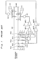
- Fig. 1 shows a conventional automatic microwave impedance matching apparatus proposed in Japanese laid open publication No. (JP-A) 63-15502/1988.
- a rectangular waveguide 100 of the automatic impedance matching apparatus is connected between a microwave oscillator and a microwave load.
- a voltage standing wave detector composed of five probes PR11 to PR15 therein aligned at an equal distance of g/8 in the longitudinal direction thereof, wherein ⁇ g is an average waveguide length of the microwave propagating in the rectangular waveguide 100.
- two pairs of composite stubs ST1 and ST2 are arranged at different positions in the longitudinal direction thereof.
- the first composite stub ST1 is composed of two stubs S11 and S12 mounted at both ends of a seesaw rod, and the stubs S11 and S12 are driven by a stub driving motor M11 so as to be inserted into and drawn out from the rectangular waveguide 100 reciprocally by a seesaw motion of the seesaw rod.
- the second composite stubs ST2 is composed of two stubs S13 and S14 mounted at both ends of another seesaw rod, and the stubs S13 and S14 are driven by another stub driving motor M12 in the same manner as the stubs S11 and S12 of the first composite stub ST1.
- a voltage standing wave of the microwave propagating in the rectangular waveguide 100 is detected by diodes DI11 to DI15 connected to the probes PR11 to PR15, respectively.
- the composed output is inputted to an input terminal of a differential amplifier AMP11 through a resistor R11.
- Each output of the diodes DI12 and DI14 is inputted to each input terminal of a differential amplifier AMP12, and the output of the diode DI13 is inputted to another input terminal of the differential amplifier AMP11.
- the output of the differential amplifier AMP11 is outputted to the stub driving motor M11 through a power amplifier AMP21, and the output of the differential amplifier AMP12 is outputted to the stub driving motor M12 through a power amplifier AMP22.
- output voltages Va11 and Va12 of respective differential amplifiers AMP11 and AMP12 are expressed by the following equations with voltages Vp11 to Vp15 of the voltage standing wave detected by respective probes PR11 to PR15.
- Va 11 Vp 11 - Vp 14
- Va 12 1 2 Vp 11 +Vp 15 -Vp 13
- the voltage standing wave in the rectangular waveguide 100 changes, namely, an impedance seen looking toward the load at the voltage standing wave detector changes. Since the probes PR11 to PR15 are arranged at an equal distance of ⁇ g/8 in the longitudinal direction of the rectangular waveguide 100, the output voltages Va11 and Va12 of respective differential amplifiers AmP11 and AMP12 are orthogonal to each other. Therefore, in the feed back system of the automatic impedance matching apparatus, the composite stubs ST1 and ST2 are driven by the stub driving motor M11 and M12 so that each of the output voltages Va11 and Va12 becomes zero. When both the output voltages Va11 and Va12 become zero, the impedance of the microwave oscillator is matched to the load impedance.
- a state of a plasma generated by the plasma generating apparatus may change suddenly, and then, a load impedance thereof may change.
- the conventional automatic impedance matching apparatus can not track the change in the load impedance thereof accurately, resulting in a hunting phenomenon therein.
- JP-A-61-1101 discloses a microwave processing apparatus utilising a control system which automatically provides triple stub tuning on a microwave line associated with a magnetron to control the sequential tuning of each of the three stubs.
- US patent no. 3617953 discloses an impedance matching device for automatically and continuously matching a time varying microwave load to a fixed frequency microwave power source and its output line.
- an automatic microwave impedance adjusting method including a first step of measuring either an impedance seen looking towards a microwave load at a predetermined reference point of a microwave transmission line of a rectangular waveguide connected between a microwave oscillator and said microwave load or a reflection coefficient thereat by detecting a voltage standing wave of a microwave propagating on said microwave transmission line;
- a whole region within a Smith chart representing an impedance seen looking towards said microwave load is divided into a first region for executing said impedance adjusting process of said third step using said first and second stubs when an impedance point seen looking towards said microwave load at said reference point is located within said first region, and a second region for executing said impedance adjusting process of said third step using said second and third stubs when said impedance point is located within said second region;
- an automatic microwave impedance adjusting apparatus for performing the above methods and comprising:
- an impedance and an admittance which are given by dividing an impedance and an admittance at a point of a rectangular waveguide 13 by a characteristic impedance of the rectangular waveguide 13 are referred to as an impedance and an admittance hereinafter, respectively.
- Fig. 3 shows the automatic microwave impedance adjusting apparatus of the preferred embodiment according to the present invention
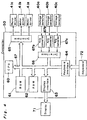
- Fig. 4 shows a controller 50 of the automatic microwave impedance adjusting apparatus and peripheral units thereof.
- the automatic microwave impedance adjusting apparatus has a single operation mode for executing only one impedance adjusting process for adjusting the reference impedance Zo to the desirable impedance Zs corresponding to the inputted desirable reflection coefficient rs without taking into consideration a change in the load impedance of the plasma generating apparatus 30, and a repeat operation mode for repeating the above impedance adjusting process with taking into consideration the change in the load impedance thereof.
- an isolator 11 for making a microwave outputted from the microwave oscillator 10 propagate toward only the plasma generating apparatus 30, a directional coupler 12, in one port of which there is mounted a diode DI10 for detecting a power of a progressive wave of the microwave propagating therein, the rectangular waveguide 13 wherein there are mounted the voltage standing wave detector 31 and the triple-stub tuner 32, a rectangular waveguide 14 wherein there is formed a hole 14h for flowing cooling air thereinto, a taper waveguide 15 for transforming the TE10 mode which is the principal mode of the isolator 11 and the rectangular waveguides 13 and 14 into the TE11 mode which is the principle mode of a circular waveguide 15, in the order of the isolator 11, the directional coupler 12, the rectangular waveguides 13 and 14 and the taper waveguide 15, in the longitudinal direction thereof. It is to be noted that a connection point of the rectangular waveguide 14 and the tape
- the power of the progressive wave of the microwave outputted from the microwave oscillator 10 is detected by the diode DI10 connected to one port of the directional coupler 12, and the detection output is inputted to a power detector 10d.
- the power detector 10d outputs a detection signal indicating a power level, which is direct proportional to the square of the detection output, to a power controller 10c.
- the power controller 10c controls the microwave oscillator 10 according to the above detection signal so that the microwave power outputted therefrom is kept a predetermined constant power level.
- the voltage standing wave detector 31 comprises three probes PR1, PR2 and PR3 which are mounted on the microwave oscillator 10 side in the rectangular waveguide 13. These probes PR1, PR2 and PR3 are mounted in the order of PR1, PR2 and PR3 from the microwave oscillator 10 side at equal spaces of ⁇ g/6 in the longitudinal direction of the rectangular waveguide 13 in the center portion of the longitudinal side of the section thereof so as to project thereinto, wherein ⁇ g is a waveguide length of the microwave propagating in the rectangular waveguide 13. Mounted points of the probes PR1, PR2 and PR3 in the longitudinal direction of the rectangular waveguide 13 are labeled Pda, Pdb and Pdc hereinafter, respectively.
- the voltage standing wave of the microwave propagating in the rectangular waveguide 13 is detected by the diodes DI1, DI2 and DI3 which are respectively connected to the probes PR1, PR2 and PR3, and respective detection outputs thereof are inputted to voltage detectors 40a, 40b and 40c, respectively.
- the voltage detectors 40a, 40b and 40c detect the voltages of the detection outputs, and output detection signals indicating detected voltage levels to analogue to digital converters (referred to as A/D converters hereinafter) 67a, 67b and 67c, respectively.
- the triple-stub tuner 32 comprises three stubs S1, S2 and S3 which are mounted on the plasma generating apparatus 30 side in the rectangular waveguide 13. These stubs S1, S2 and S3 are mounted in the order of S1, S2 and 53 from the microwave oscillator 10 side at equal spaces of ⁇ g/4 in the longitudinal direction of the rectangular waveguide 13 in the center portion of the longitudinal side of the section thereof so as to be inserted into and drawn out from the rectangular waveguide 13 in a direction perpendicular to the longitudinal side of the section thereof.
- the stub S1 is mounted at a mounted point Ps1 apart by a distance of ⁇ g/2 in the longitudinal direction of the rectangular waveguide 13 from the mounted point Pda of the probe PR1 of the voltage standing wave detector 31.
- Mounted points of respective stubs S1, S2 and S3 are labeled Ps1, Ps2 and Ps3 in the longitudinal direction of the rectangular waveguide 13.
- pulse signals indicating the insertion lengths or the drawing-out lengths of respective stubs S1, S2 and S3 to be inserted into or drawn out from the rectangular waveguide 13, and polarity signals indicating the insertion or the drawing-out operation thereof are outputted from an interface 65 of the controller 50 to respective motor drivers 41a, 41b and 41c. Responsive to these signals, the motor drivers 41a, 41b and 41c amplify the pulse signals, and output the amplified pulse signals having polarities indicated by the above polarity signals to the stepping motors M1, M2 and M3, respectively.
- the stepping motors M1, M2 and M3 respectively drive the stubs S1, S2 and S3 according to the pulse signals so as to insert them into the rectangular waveguide 13 by insertion lengths corresponding to the pulse numbers of the pulse signals, or draw out them therefrom by drawing-out lengths corresponding to the pulse numbers of the pulse signals.
- the plasma generating apparatus 30 is provided for performing an oxidation process for a high temperature superconductor W of oxide group.
- an electromagnet 17 for applying a magnetic field onto a glass plasma container 18g having a half egg shape which is mounted in the center portion of the circular waveguide 16, in order to not only generate a plasma utilizing an electron cyclotron motion but also store the generated plasma effectively within the plasma container 18g.
- a cooling air outlet 16a for exhausting the cooling air which has been flowed from the hole 14h of the rectangular waveguide 14 into the outside of the circular waveguide 16.
- cooling air is flowed thereinto in order to prevent the temperature of the plasma container 18g from increasing when the plasma container 18g receives an energy from the plasma generated therein, so as to prevent the plasma container 18g from being broken due to the over heating.
- a plasma outlet 20 for flowing out the plasma generated in the plasma container 18g into the plasma chamber 18.
- a ring-shaped electrode 20a which is electrically connected to a positive electrode of a direct-current voltage source 21 and ground.
- a negative electrode of the direct-current voltage source 21 is electrically connected to a support mechanism 19m.
- a table 19 for mounting the superconductor W to be processed.
- the table 19 is connected to the support mechanism 19m for moving the table 19 in directions as indicated by arrows 19a. Further, in the positions opposing to each other of the outer peripheral portion of the plasma processing chamber 18, there are formed an oxygen gas inlet 18h for supplying oxygen gas into the plasma processing chamber 18, and an oxygen gas outlet 18j for exhausting the supplied oxygen gas into the outside of the plasma processing chamber 18.
- the inside of the plasma processing chamber 18 is kept at an oxygen gas pressure in the range from 10 ⁇ 4 Torr to 10 ⁇ Torr, and then, the superconductor W to be processed is heated at a temperature in the range from 200 °C to 400 °C.
- a microwave having a frequency such as 2.45 GHz is generated by the microwave oscillator 10. The generated microwave propagates in the isolator 11, the directional coupler 12, the rectangular waveguides 13 and 14, the taper waveguide 15, and the circular waveguide 16, and is incident to the plasma processing chamber 18.
- a magnetic field is applied to the microwave incident into the circular waveguide 16 in a direction perpendicular to the propagation direction of the microwave by the electromagnet 17, so as to generate an electron cyclotron resonance for the incident microwave at the position on the left side in Fig. 3 of the superconductor W to be processed which is arranged in the plasma processing chamber 18.
- a negative voltage such as a voltage in the range from -5 V to -100 V is applied to the ring-shaped electrode 20a mounted on the outer peripheral portion of the plasma outlet 20 relative to a potential of the table 19 on which the superconductor W to be processed is mounted.
- Fig. 4 shows the controller 50 for controlling the operation of the automatic microwave impedance adjusting apparatus and the peripheral units thereof.
- the controller 50 comprises a central processing unit (referred to as a CPU hereinafter) 60 for controlling the impedance adjusting process of the automatic microwave impedance adjusting apparatus, a read only memory (referred to as a ROM hereinafter) 61 for storing a system program for executing the process of the CPU 60 and data required for executing the above system program, and a random access memory (referred to as a RAM hereinafter) 62 for being used as a working area and storing data required in the processing of the CPU 60.
- a CPU central processing unit
- a ROM read only memory
- RAM random access memory
- the controller 50 further comprises a display interface 63 connected to a display 71, a keyboard interface 64 connected to the keyboard 72, the A/D converters 67a, 67b and 67c, an interface 66 connected to the A/D converters 67a, 67b and 67c, and an interface 65 connected to the motor drivers 41a, 41b and 41c.
- the CPU 60, the ROM 61, the RAM 62, the display interface 63, the keyboard interface 64 and the interfaces 65 and 66 are connected to each other through a bus 67.
- Respective detection signals outputted from the voltage detectors 40a, 40b and 40c are A/D converted to digital data, and then, the digital data are transferred to the RAM through the interface 66 and the bus 67, and are stored therein.
- the CPU 60 calculates data of the insertion lengths or the drawing-out lengths of respective stubs S1, S2 and S3 required for adjusting the reference impedance Zo seen looking toward the load at the reference point Ps1 to the above desirable impedance Zs from the digital data of the detection signals, and a desirable reflection coefficient ⁇ s which has been previously inputted using the keyboard 72, and outputs the calculated data and data indicating the insertion or the drawing-out operation of respective stubs S1, S2 and S3, to the interface 65 through the bus 67.
- the interface 65 Responsive to the data, the interface 65 generates the pulse signals indicating the insertion lengths or the drawing-out lengths of respective stubs S1, S2 and S3 to be inserted into or drawn out from the rectangular waveguide 13, and the polarity signals indicating the insertion or the drawing-out operation thereof, to respective motor drivers 41a, 41b and 41c. It is to be noted that the impedance adjusting process executed by the CPU 60 will be described in detail later, with reference to flowcharts shown in Figs. 22 to 24.
- the display 71 displays impedance points seen looking toward the load on a Smith chart, and the insertion lengths of respective stubs S1, S2 and S3, according to the data inputted from the CPU 60 through the display interface 63.
- the keyboard 72 comprises a operation mode selection key (not shown) for selecting either the repeat operation mode or the single operation mode, and a set of ten keys (not shown) for inputting the absolute value
- the voltage standing wave detector 31 comprises three probes PR1, PR2 and PR3 mounted at respective points Pda, Pdb and Pdc in the longitudinal direction of the rectangular waveguide 13 at equal spaces of ⁇ g/6, as described above.
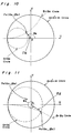
- Fig. 5 shows a voltage standing wave pattern
- of the voltage standing wave changes periodically with a period of ⁇ g/2.
- the amplitudes of the voltage standing wave at the points Pda, Pdb and Pdc are labeled
- Fig. 6 is a crank diagram showing a relationship among vectors V ⁇ a, V ⁇ b and V ⁇ c of the amplitudes Va, Vb and Vc of the voltage standing wave, a vector D ⁇ of a progressive wave voltage D, and a vector E ⁇ of a reflected wave voltage E.
- ⁇ o is a phase of the reflected wave voltage E relative to a point where the amplitude
- the reflection coefficient ⁇ o expressed by the above equation (3) is a reflection coefficient at the reference point Ps1.
- respective vectors V ⁇ a, V ⁇ b and V ⁇ c of the amplitudes of the voltage standing wave are a sum of the vector D ⁇ of the progressive wave voltage D and the vector E ⁇ of the reflected voltage E.
- Respective end points of the vector V ⁇ a, V ⁇ b and V ⁇ c are positioned on a circle having a radius equal to the amplitude of the vector E ⁇ of the reflected wave voltage E and a center point which is located at the end point Pdd of the vector D ⁇ of the progressive wave voltage D so that each difference between respective phases thereof becomes 2 3 ⁇ .
- and the phase ⁇ o of the reflection coefficient ⁇ o can be obtained by calculating the solutions of the simultaneous equations (4) to (7). Furthermore, the admittance or the impedance seen looking toward the plasma generating apparatus 30 at the reference point Ps1 can be calculated using equations (9) to (11) which are described later, from the absolute value
- the triple-stub tuner 32 comprises three stubs S1, S2 and S3 mounted at respective points Ps1, Ps2 and Ps3 of the rectangular waveguide 13 at equal spaces of ⁇ g/4 in the longitudinal direction thereof, as described above.
- Fig. 21 shows a relationship between an insertion length L of each of the stubs S1, S2 and S3 when inserted into the rectangular waveguide 13, and a susceptance B connected to the mounted point of each stub in the rectangular waveguide 13.
- each of the stubs S1, S2 and S3 operates as an admittance element having a pure susceptance B.
- Fig. 7 shows an equivalent circuit of the triple-stub tuner 32 which is connected between the microwave oscillator 10 and the plasma generating apparatus 30.
- the automatic microwave impedance adjusting apparatus of the present preferred embodiment there is calculated the insertion lengths of respective stubs S1, S2 and S3 required for adjusting the admittance Yo seen looking toward the load of the plasma generating apparatus 30 at the reference point Ps1 to a desirable admittance Ys including the admittance Yso seen looking toward the microwave oscillator 10 at the reference point Ps1, by the CPU 60 of the controller 50, and then, the stepping motors M1, M2 and M3 are driven so that the stubs S1, S2 and S3 are inserted into the rectangular waveguide 13 by the calculated insertion lengths, respectively.
- Fig. 8 shows a relationship between a Smith chart and a UV orthogonal coordinates (referred to as a UV coordinates hereinafter) of a complex plane of a reflection coefficient ⁇ .
- ⁇ e j ⁇ o u o + jv o
- u o and v o are a coordinate value of the U-axis and a coordinate value of the V-axis of the UV coordinates.
- UV coordinates of an admittance point located on the Smith chart are represented hereinafter by a coordinate representation with a suffix "uv” such as (0, j)uv, (1, j0)uv, and also, coordinates of an admittance point located on the Smith chart which indicate a conductance and a susceptance thereof is represented hereinafter by a coordinate representation without any suffix such as (Go, jBo).
- the susceptance Bo' of the admittance Yo' seen looking toward the load at the point Ps2 of the stub S2 is calculated from the UV coordinates of the admittance point Po of the admittance Yo seen looking toward the load at the reference point Ps1, and also, the susceptance Bo of the admittance Yo seen looking toward the load at the reference point Ps1 is calculated from the UV coordinates of the admittance point Pp' of the admittance Yo' seen looking toward the load at the point Ps2 of the stub S2.
- the converted susceptance can be calculated by inverting respective signs of the coordinate values of the U-axis and V-axis and substituting the inverted UV coordinates into the equation (11).
- Fig. 22 is flowchart showing a main routine of an impedance adjusting process executed by the CPU 60 of the controller 50.
- the main routine includes two subroutines executed at steps #7 and #8 of Fig. 22.
- step #1 either the repeat operation mode or the single operation mode is selected using the operation mode selection key of the keyboard 72, and then, at step #2, an absolute value
- the CPU 60 calculates a conductance Gs and a susceptance Bs of a desirable admittance Ys corresponding to the inputted reflection coefficient ⁇ s, using the equations (9) to (11) from the absolute value
- step #4 there are calculated the amplitudes of the voltage standing wave
- step #6 it is judged whether the admittance point Po of the reference admittance Yo detected by the voltage standing wave detector 31 is located within a tuning region Rx1 shown in Fig. 12, or a tuning region Ry1 shown in Fig. 15. Then, if the admittance point Po is located within the tuning region Rx1, the program flow goes to step #7, and then, the impedance adjusting process using the stubs S2 and S3 is executed so as to adjust the reference admittance Yo to the above desirable admittance Ys, and the program flow goes to step #9.
- the program flow goes to step #8, and then, the impedance adjusting process using the stubs S1 and S2 is executed so as to adjust the reference admittance Yo to the above desirable admittance Ys, and the program flow goes to step #9.
- step #9 it is judged whether or not the operation mode is set at the repeat operation mode. If the operation mode is set at the repeat operation mode, the program flow goes to step #4, and then, the processes from steps #4 are repeated. On the other hand, if the operation mode is set at the single operation mode, the impedance adjusting mode is completed.
- the repeat operation mode is useful for adjusting the impedance seen looking toward the load having a load impedance changing with a time such as the plasma generating apparatus 30. Namely, at a time t0, there is calculated reflection coefficient ro corresponding to the reference admittance Yo in the processes of steps #4 and #5. However, if the load impedance at a time t1 defined after the time t0 is shifted from the load impedance at the time t0, the reference admittance Yo after executing the impedance adjusting process at step #7 or #8 is mismatched to the desirable admittance Ys corresponding to the desirable reflection coefficient rs which has been previously inputted at step #2.
- the automatic microwave impedance adjusting apparatus has such an advantage that the impedance adjusting process can be executed depending on a change in the load impedance of the load such as the plasma generating apparatus 30, even though the load impedance changes.
- step #2 In order to match the impedance seen looking toward the microwave oscillator 10 to the impedance seen looking toward the load of the plasma generating apparatus 30, at step #2, "zero” and “any number” are inputted as the absolute value
- the reference impedance seen looking toward the load may not become a certain desirable impedance stably due to a frequent change in the load impedance of the plasma generating apparatus 30, even though the impedance adjusting process of the present preferred embodiment is executed so that the reference impedance seen looking toward the load at the reference point Ps1 is matched to the impedance seen toward the microwave oscillator 10.
- step #2 there are inputted an absolute value
- Fig. 23 is a flowchart showing the subroutine of the impedance adjusting process using the stubs S2 and S3 (step #7 of Fig. 22).
- step #11 there is calculated a susceptance Bo seen looking toward the load at the reference point Ps1 using the equations (8) and (11) from the absolute value
- step #15 there is calculated a susceptance Ba' seen looking toward the load at the point Ps2 of the stub S2 using the equation (11), as described above, from the UV coordinates of the above susceptance Ba.
- step #17 there are calculated insertion lengths of the stubs S2 and S3 using the relationship between the insertion length L thereof and the susceptance B shown in Fig. 21 which has been previously measured, from the calculated susceptances B20' and B30, and then, at step #18, the stepping motors M2 and M3 are driven, respectively, so that the stubs S2 and S3 are inserted into the rectangular waveguide 13 by the calculated insertion lengths. Then, the reference admittance Yo is adjusted to the desirable admittance Ys.
- Fig. 24 is a flowchart showing the subroutine of the impedance adjusting process using the stubs S1 and S2 (step #8 of Fig. 22).
- step #21 there is calculated a susceptance Bo' seen looking toward the load at the point Ps2 using the equations (15) and (16) from the absolute value
- step #25 there is calculated a susceptance Bb seen looking toward the load at the reference point Ps1 using the equation (11), as described above, from the UV coordinates of the above susceptance Bb'.
- step #27 there are calculated insertion lengths of the stubs S1 and S2 using the relationship between the insertion length L thereof and the susceptance B shown in Fig. 21 which has been previously measured, from the calculated susceptances B10 and B20', and then, at step #28, the stepping motors M1 and M2 are driven, respectively, so that the stubs S1 and S2 are inserted into the rectangular waveguide 13 by the calculated insertion lengths. Then, the reference admittance Yo is adjusted to the desirable admittance Ys.
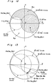
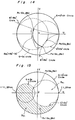
- the tuning region Rx0 is a region where the impedance matching process is executed using the stubs S2 and S3 when the admittance point Po of the reference admittance Yo is located within the tuning region Rx0 on the Smith chart
- the tuning region Ry0 is a region where the impedance matching process is executed using the stubs S1 and S2 when the admittance point Po of the reference admittance Yo is located within the tuning region Ry0 on the Smith chart.
- the impedance matching process shown in Fig. 18 is executed in a manner similar to that of the subroutine of step #7, and the impedance matching process shown in Fig. 19 is executed in a manner similar to that of the subroutine of step #8.
- step #6 of the present preferred embodiment it is judged whether the admittance point Po of the reference admittance Yo is located within the tuning region Rx1 or Ry1, and then, the impedance adjusting process using the stubs S2 and S3 is executed if the point Po is located within the tuning region Rx1, on the other hand, the impedance adjusting process using the stubs S1 and S2 is executed if the point Po is located within the tuning region Ry1.
- the present invention is not limited to this.
- an impedance adjusting process may be executed using all the stubs S1, S2 and S3. Then, the reference admittance Yo can be adjusted to a desirable admittance Ys, for a time shorter than that of the impedance adjusting process using the stubs S1 and S2, in the above case.
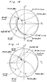
- Fig. 18 is a Smith chart and a complex plane of a UV coordinates showing an operation of an impedance matching process using all the stubs S1, S2 and S3.
- the susceptances of respective stubs S1, S2 and S3 are changed so as to match the reference admittance Yo to the admittance Yso seen looking toward the microwave oscillator 10 at the reference points Ps1.
- the calculation of this impedance matching process is executed in a manner similar to that of the subroutine of step #7 or #8.
- the present invention there are calculated the absolute value
- the present invention is not limited to this.
- a reflection coefficient corresponding to the measured impedance may be calculated, and then, the impedance adjusting process of the present invention may be executed.
- three probes PR1, PR2 and PR3 are mounted at equal spaces of ⁇ g/6 in the longitudinal direction of the rectangular waveguide 13.
- the present invention is not limited to this.
- At least three probes may be mounted at different points at predetermined spaces, one of which is not a product of any natural number and the length ⁇ g/2.
- Each space between the probes is preferably set at a length equal to a product of any natural number and the length ⁇ g/6 except for products of any natural number and the length ⁇ g/2.
- the space in the longitudinal direction of the rectangular waveguide 13 between the stub S1 and the probe PR1 is set at the length ⁇ g/2 for convenience of the explanation.
- This space may be set at any distance.
- step #2 of Fig. 22 of the present preferred embodiment there are inputted the absolute value
- the present invention is not limited to this.
- a resistance Rs and a reactance Xs of a desirable impedance Zs may be in putted, or a conductance Gs and a susceptance Bs of a desirable admittance Ys corresponding to a desirable impedance Zs may be inputted.
Landscapes
- Plasma Technology (AREA)
- Constitution Of High-Frequency Heating (AREA)
Description
- The present invention relates to an automatic impedance adjusting apparatus for a microwave load and an automatic impedance adjusting method therefor, and more particularly to an automatic impedance adjusting apparatus for adjusting an impedance seen looking towards a microwave load at a point of a microwave transmission line to a desirable impedance such as an impedance of a microwave oscillator, and an automatic impedance adjusting method therefor.
- Fig. 1 shows a conventional automatic microwave impedance matching apparatus proposed in Japanese laid open publication No. (JP-A) 63-15502/1988.
- Referring to Fig. 1, a
rectangular waveguide 100 of the automatic impedance matching apparatus is connected between a microwave oscillator and a microwave load. On the microwave oscillator side in therectangular waveguide 100, there is arranged a voltage standing wave detector composed of five probes PR11 to PR15 therein aligned at an equal distance of g/8 in the longitudinal direction thereof, wherein λg is an average waveguide length of the microwave propagating in therectangular waveguide 100. On the microwave load side in therectangular waveguide 100, two pairs of composite stubs ST1 and ST2 are arranged at different positions in the longitudinal direction thereof. - The first composite stub ST1 is composed of two stubs S11 and S12 mounted at both ends of a seesaw rod, and the stubs S11 and S12 are driven by a stub driving motor M11 so as to be inserted into and drawn out from the
rectangular waveguide 100 reciprocally by a seesaw motion of the seesaw rod. On the other hand, the second composite stubs ST2 is composed of two stubs S13 and S14 mounted at both ends of another seesaw rod, and the stubs S13 and S14 are driven by another stub driving motor M12 in the same manner as the stubs S11 and S12 of the first composite stub ST1. - A voltage standing wave of the microwave propagating in the
rectangular waveguide 100 is detected by diodes DI11 to DI15 connected to the probes PR11 to PR15, respectively. After the output of the diode DI11 is outputted to the anode of the diode DI15 so as to compose the output of the diode DI15 therewith, the composed output is inputted to an input terminal of a differential amplifier AMP11 through a resistor R11. Each output of the diodes DI12 and DI14 is inputted to each input terminal of a differential amplifier AMP12, and the output of the diode DI13 is inputted to another input terminal of the differential amplifier AMP11. - The output of the differential amplifier AMP11 is outputted to the stub driving motor M11 through a power amplifier AMP21, and the output of the differential amplifier AMP12 is outputted to the stub driving motor M12 through a power amplifier AMP22.
- In the automatic microwave impedance matching apparatus constructed above, output voltages Va₁₁ and Va₁₂ of respective differential amplifiers AMP11 and AMP12 are expressed by the following equations with voltages Vp₁₁ to Vp₁₅ of the voltage standing wave detected by respective probes PR11 to PR15.


- When the stub driving motors M11 and M12 are driven according to the output voltages Va₁₁ and Va₁₂, respectively, the voltage standing wave in the
rectangular waveguide 100 changes, namely, an impedance seen looking toward the load at the voltage standing wave detector changes. Since the probes PR11 to PR15 are arranged at an equal distance of λg/8 in the longitudinal direction of therectangular waveguide 100, the output voltages Va₁₁ and Va₁₂ of respective differential amplifiers AmP11 and AMP12 are orthogonal to each other. Therefore, in the feed back system of the automatic impedance matching apparatus, the composite stubs ST1 and ST2 are driven by the stub driving motor M11 and M12 so that each of the output voltages Va₁₁ and Va₁₂ becomes zero. When both the output voltages Va₁₁ and Va₁₂ become zero, the impedance of the microwave oscillator is matched to the load impedance. - However, when the above automatic microwave impedance matching apparatus is applied to an apparatus comprising a plasma generating apparatus such as a plasma etching apparatus, a plasma CVD apparatus or the like, the following problems are caused.
- (1) A state of a plasma generated by the plasma generating apparatus may change suddenly, and then, a load impedance thereof may change. In this case, the conventional automatic impedance matching apparatus can not track the change in the load impedance thereof accurately, resulting in a hunting phenomenon therein.
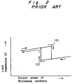
- (2) As shown in Fig. 2, there is a hysteresis in a relationship between an output power of the microwave oscillator and a load impedance of the plasma generating apparatus, and particularly, the hysteresis has two
discontinuous points discontinuous points - It is known to those skilled in the art that a plasma may be generated more stably in a state slightly shifted from the impedance matching state. Therefore, it has been desired that the impedance seen looking towards the load is automatically adjusted to a desirable impedance. However, the automatic microwave impedance matching apparatus described above cannot adjust the impedance seen looking towards the load to a desirable impedance.
- Japanese laid-open publication no. JP-A-61-1101 discloses a microwave processing apparatus utilising a control system which automatically provides triple stub tuning on a microwave line associated with a magnetron to control the sequential tuning of each of the three stubs.
- US patent no. 3617953 discloses an impedance matching device for automatically and continuously matching a time varying microwave load to a fixed frequency microwave power source and its output line.
- Attention is also directed to Patents Abstracts of Japan, vol. 10, no. 137 (E405)(2194) 21 May 1986, and JP-A-61 1101 (Fijitsu K.K.) 07 January 1986, and to 'Foundations for Microwave Engineering', International Student Edition, McGraw-Hill Physical and Quantum Electronics Series, R.E. Collin, 1966, pages 212-217.
- It would be desirable to be able to provide an automatic impedance adjusting method and/or apparatus capable of more stably and more precisely adjusting an impedance seen looking towards a microwave load to a desirable impedance such as an impedance of a microwave oscillator, even if the load impedance changes.
- According to one aspect of the present invention there is provided an automatic microwave impedance adjusting method including a first step of measuring either an impedance seen looking towards a microwave load at a predetermined reference point of a microwave transmission line of a rectangular waveguide connected between a microwave oscillator and said microwave load or a reflection coefficient thereat by detecting a voltage standing wave of a microwave propagating on said microwave transmission line;
- wherein said method includes:
- a second step of calculating insertion lengths of first to third stubs of variable impedance means so as to adjust said impedance seen looking towards said microwave load to a desired value corresponding to an inputted desired reflection coefficient, responsive to said value measured at said first step, said first to third stubs being mounted on said microwave load side of said reference point on said microwave transmission line, and mounted at different points in an order of said first to third stubs at equal spaces of a quarter of said waveguide length in the longitudinal direction of said rectangular waveguide, and
- a third step of inserting said first to third stubs into said rectangular waveguide by insertion lengths calculated at said second step, thereby adjusting said impedance seen looking towards said microwave load to said desired value,
- characterised in that a whole region within a Smith chart representing an impedance seen looking towards said microwave load is divided into a first region for executing said impedance adjusting process of said third step using first and second stubs when an impedance point seen looking towards said microwave load at said reference point is located within said first region, a second region for executing said impedance adjusting process of said third step using said second and third stubs when said impedance point is located within said second region, and a third region for executing said impedance adjusting of said third step using all said first to third stubs when said impedance point is located within said third region, said third region being defined as a partial region of said first region for any positive coordinate value of a V-axis of a UV orthogonal coordinate of the Smith chart; and
- wherein said second step includes:
- calculating an impedance seen looking towards said microwave load at said reference point responsive to said value measured at said first step; and
- judging whether an impedance point of said calculated impedance is located within either said first region, said second region or said third region on said Smith chart; and
- wherein said third step includes:
- executing said impedance adjusting process of said third step using said first and second stubs when it is judged that said impedance point of said calculated impedance is located within said first region, executing said impedance adjusting process of said third step using said second and third stubs when it is judged that said impedance point of said calculated impedance is located within said second region, and executing said impedance adjusting process of said third step using all said first to third stubs when it is judged that said impedance point of said calculated impedance is located within said third region.
- There is also provided a method according to the one aspect of the invention wherein a whole region within a Smith chart representing an impedance seen looking towards said microwave load is divided into a first region for executing said impedance adjusting process of said third step using said first and second stubs when an impedance point seen looking towards said microwave load at said reference point is located within said first region, and a second region for executing said impedance adjusting process of said third step using said second and third stubs when said impedance point is located within said second region;
- wherein said second step includes:
- calculating an impedance seen looking towards said microwave load at said reference point responsive to said value measured at said first step, and
- judging whether an impedance point of said calculated impedance is located within either said first region or said second region of said Smith chart, and
- wherein said third step includes:
- executing said impedance adjusting process of said third step using said first and second stubs when it is judged that said impedance point of said calculated impedance is located within said first region, and executing said impedance adjusting process of said third step using said second and third stubs when it is judged that said impedance point of said calculated impedance is located within said second region.
- In all said methods, the processes of said first to third steps may be repeated.
- According to a further aspect of the invention, there is provided an automatic microwave impedance adjusting apparatus for performing the above methods and comprising:
- a microwave transmission line connected between a microwave oscillator and a microwave load, said microwave transmission line being a rectangular waveguide,
- measuring means for measuring either an impedance seen looking towards said microwave load at a mounted point thereof or a reflection coefficient thereat by detecting a voltage standing wave of a microwave propagating on said microwave transmission line,
- variable impedance means for changing an impedance to be connected to a mounted point thereof, and
- control means for controlling said variable impedance means responsive to a value measured by said measuring means so as to adjust said impedance to a desired value corresponding to an inputted desired reflection coefficient,
- characterised in that
- said variable impedance means are mounted on said microwave load side of said measuring means on said microwave transmission line, said variable impedance means comprising three stubs mounted at different points at equal spaces of a quarter of said waveguide wavelength in the longitudinal direction of said rectangular waveguide, and
- said control means comprises:
- calculating means for calculating insertion lengths of first to third stubs of variable impedance means so as to adjust said impedance seen looking towards said microwave load to a desired value corresponding to an inputted desired reflection coefficient, responsive to said value measured by said measuring means, and
- insertion control means for inserting said first to third stubs into said rectangular waveguide by insertion lengths calculated by said calculating means, thereby adjusting said impedance seen looking towards said microwave load to said desired value,
- wherein a whole region within a Smith chart representing an impedance seen looking towards said microwave load is divided into a first region for executing said impedance adjusting process of said insertion control means using first and second stubs when an impedance point seen looking towards said microwave load at said reference point is located within said first region, a second region for executing said impedance adjusting process of said insertion control means using said second and third stubs when said impedance point is located within said second region, and a third region for executing said impedance adjusting of said insertion control means using all said first to third stubs when said impedance point is located within said third region, said third region being defined as a partial region of said first region for any positive coordinate value of a V-axis of a UV orthogonal coordinate of the Smith chart; and
- wherein said calculating means comprises:
- means for calculating an impedance seen looking towards said microwave load at said reference point responsive to said value measured by said measuring means; and
- means for judging whether an impedance point of said calculated impedance is located within either said first region, said second region or said third region on said Smith chart; and
- wherein said insertion control means comprises:
- executing said impedance adjusting process of said insertion control means using said first and second stubs when it is judged that said impedance point of said calculated impedance is located within said first region, executing said impedance adjusting process of said insertion control means using said second and third stubs when it is judged that said impedance point of said calculated impedance is located within said second region, and executing said impedance adjusting process of said insertion control means using all said first to third stubs when it is judged that said impedance point of said calculated impedance is located within said third region.
- By way of example only, the apparatus and method of the invention will now be described in greater detail with reference to the accompanying drawings of which:
- Fig. 1 is a schematic diagram showing a conventional automatic microwave impedance matching apparatus;
- Fig. 2 is a graph showing a relationship between a output power of a microwave oscillator and a load impedance |Z| of a plasma generating apparatus;
- Fig. 3 is a schematic diagram showing an automatic microwave impedance adjusting apparatus of a preferred embodiment according to the present invention;
- Fig. 4 is a schematic block diagram showing a controller of the automatic microwave impedance adjusting apparatus shown in Fig. 3 and peripheral units thereof;
- Fig. 5 is a chart showing a voltage standing wave pattern in a rectangular waveguide shown in Fig. 3;
- Fig. 6 is a crank diagram showing respective vectors of the voltage standing wave at mounted points of respective probes shown in Fig. 3;
- Fig. 7 is a circuit diagram showing an equivalent circuit of a triple-stub tuner arranged between the microwave oscillator and the plasma generating apparatus shown in Fig. 3;
- Figs. 8 and 9 are reflection coefficient charts and Smith charts showing an admittance contour thereon when stubs S1, S2 and S3 of the triple-stub tuner shown in Fig. 3 are inserted into and drawn out from the rectangular waveguide;
- Figs. 10 to 20 are reflection coefficient charts and Smith charts showing an action of the automatic microwave impedance adjusting apparatus shown in Figs. 1 and 2;
- Fig. 21 is a graph showing a relationship between an insertion length of each stub of the triple-stub tuner shown in Fig. 1 when inserted into the rectangular waveguide, and a susceptance connected to the stub point;
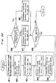
- Fig. 22 is a flowchart showing a main routine of an automatic impedance adjusting process executed by a CPU of the controller shown in Fig. 4;
- Fig. 23 is a flowchart showing a subroutine of an impedance adjusting process using stubs S2 and S3; and
- Fig. 24 is a flowchart showing a subroutine of an impedance adjusting process using stubs S1 and S1.
- An automatic microwave impedance adjusting apparatus of a preferred embodiment according to the present invention will be described below, in the order of the following items, with reference to the attached drawings.
- (1) Composition of an automatic impedance adjusting apparatus
- (2) Composition of a controller and peripheral units thereof
- (3) Voltage standing wave detector
- (4) Triple-stub tuner
- (5) Action of the automatic impedance adjusting apparatus
- (6) Impedance matching process
- (7) Modifications
- It is to be noted that, in this specification, a normalized impedance and a normalized admittance which are given by dividing an impedance and an admittance at a point of a
rectangular waveguide 13 by a characteristic impedance of therectangular waveguide 13 are referred to as an impedance and an admittance hereinafter, respectively. - Fig. 3 shows the automatic microwave impedance adjusting apparatus of the preferred embodiment according to the present invention, and Fig. 4 shows a
controller 50 of the automatic microwave impedance adjusting apparatus and peripheral units thereof. - The automatic microwave impedance adjusting apparatus of the present preferred embodiment mainly comprises:
- (a) a voltage
standing wave detector 31 composed of three probes PR1, PR2 and PR3 for detecting an amplitude of a voltage standing wave of a microwave propagating in therectangular waveguide 13 which is connected between amicrowave oscillator 10 and aplasma generating apparatus 30, the voltagestanding wave detector 13 being arranged on themicrowave oscillator 10 side in therectangular waveguide 13; - (b) a triple-
stub tuner 32 composed of three stubs S1, S2 and S3 for connecting an admittance in parallel to the transmission line of therectangular waveguide 13 when driven by stepping motors M1, M2 and M3, the triple-stub tuner 32 being arranged on theplasma generating apparatus 30 side in therectangular waveguide 13; and - (c) the
controller 50 for calculating a reflection coefficient ro at the probe PR1 of the voltagestanding wave detector 31 from amplitudes of the voltage standing wave detected by the voltagestanding wave detector 31, calculating a desirable admittance Ys corresponding to a desirable reflection coefficient Γs which has been previously inputted using akeyboard 72, calculating insertion lengths of the stubs S1, S2 and S3 required for adjusting an admittance Yo seen looking toward a load of theplasma generating apparatus 30 at a mounted point Ps₁ of the stub S1 mounted in the rectangular waveguide 13 (referred to as a reference point hereinafter) to the calculated desirable admittance Ys, and outputting driving signals for driving the stepping motors M1, M2 and M3 so that the stubs S1, S2 and S3 are inserted into therectangular waveguide 13 by the above calculated insertion lengths, respectively; and - the automatic microwave impedance adjusting apparatus is characterized in that an impedance (referred to as a reference impedance hereinafter) Zo seen looking toward the
plasma generating apparatus 30 at the reference point Ps₁ is automatically adjusted to a desirable impedance Zs corresponding to the inputted desirable reflection coefficient Γs. - The automatic microwave impedance adjusting apparatus has a single operation mode for executing only one impedance adjusting process for adjusting the reference impedance Zo to the desirable impedance Zs corresponding to the inputted desirable reflection coefficient rs without taking into consideration a change in the load impedance of the
plasma generating apparatus 30, and a repeat operation mode for repeating the above impedance adjusting process with taking into consideration the change in the load impedance thereof. - Referring to Fig. 3, between the
microwave oscillator 10 and theplasma generating apparatus 30, there are connected anisolator 11 for making a microwave outputted from themicrowave oscillator 10 propagate toward only theplasma generating apparatus 30, adirectional coupler 12, in one port of which there is mounted a diode DI10 for detecting a power of a progressive wave of the microwave propagating therein, therectangular waveguide 13 wherein there are mounted the voltagestanding wave detector 31 and the triple-stub tuner 32, arectangular waveguide 14 wherein there is formed ahole 14h for flowing cooling air thereinto, ataper waveguide 15 for transforming the TE₁₀ mode which is the principal mode of theisolator 11 and therectangular waveguides circular waveguide 15, in the order of theisolator 11, thedirectional coupler 12, therectangular waveguides taper waveguide 15, in the longitudinal direction thereof. It is to be noted that a connection point of therectangular waveguide 14 and thetaper waveguide 15 is referred to as aload end 14t seen looking at therectangular waveguide 13 of the automatic microwave impedance adjusting apparatus. - The power of the progressive wave of the microwave outputted from the
microwave oscillator 10 is detected by the diode DI10 connected to one port of thedirectional coupler 12, and the detection output is inputted to apower detector 10d. Thepower detector 10d outputs a detection signal indicating a power level, which is direct proportional to the square of the detection output, to apower controller 10c. Thepower controller 10c controls themicrowave oscillator 10 according to the above detection signal so that the microwave power outputted therefrom is kept a predetermined constant power level. - The voltage
standing wave detector 31 comprises three probes PR1, PR2 and PR3 which are mounted on themicrowave oscillator 10 side in therectangular waveguide 13. These probes PR1, PR2 and PR3 are mounted in the order of PR1, PR2 and PR3 from themicrowave oscillator 10 side at equal spaces of λg/6 in the longitudinal direction of therectangular waveguide 13 in the center portion of the longitudinal side of the section thereof so as to project thereinto, wherein λg is a waveguide length of the microwave propagating in therectangular waveguide 13. Mounted points of the probes PR1, PR2 and PR3 in the longitudinal direction of therectangular waveguide 13 are labeled Pda, Pdb and Pdc hereinafter, respectively. - The voltage standing wave of the microwave propagating in the
rectangular waveguide 13 is detected by the diodes DI1, DI2 and DI3 which are respectively connected to the probes PR1, PR2 and PR3, and respective detection outputs thereof are inputted tovoltage detectors voltage detectors - The triple-
stub tuner 32 comprises three stubs S1, S2 and S3 which are mounted on theplasma generating apparatus 30 side in therectangular waveguide 13. These stubs S1, S2 and S3 are mounted in the order of S1, S2 and 53 from themicrowave oscillator 10 side at equal spaces of λg/4 in the longitudinal direction of therectangular waveguide 13 in the center portion of the longitudinal side of the section thereof so as to be inserted into and drawn out from therectangular waveguide 13 in a direction perpendicular to the longitudinal side of the section thereof. It is to be noted that the stub S1 is mounted at a mounted point Ps₁ apart by a distance of λg/2 in the longitudinal direction of therectangular waveguide 13 from the mounted point Pda of the probe PR1 of the voltagestanding wave detector 31. Mounted points of respective stubs S1, S2 and S3 are labeled Ps₁, Ps₂ and Ps₃ in the longitudinal direction of therectangular waveguide 13. - As described later, pulse signals indicating the insertion lengths or the drawing-out lengths of respective stubs S1, S2 and S3 to be inserted into or drawn out from the
rectangular waveguide 13, and polarity signals indicating the insertion or the drawing-out operation thereof are outputted from aninterface 65 of thecontroller 50 torespective motor drivers 41a, 41b and 41c. Responsive to these signals, themotor drivers 41a, 41b and 41c amplify the pulse signals, and output the amplified pulse signals having polarities indicated by the above polarity signals to the stepping motors M1, M2 and M3, respectively. The stepping motors M1, M2 and M3 respectively drive the stubs S1, S2 and S3 according to the pulse signals so as to insert them into therectangular waveguide 13 by insertion lengths corresponding to the pulse numbers of the pulse signals, or draw out them therefrom by drawing-out lengths corresponding to the pulse numbers of the pulse signals. - The
plasma generating apparatus 30 is provided for performing an oxidation process for a high temperature superconductor W of oxide group. On the outer peripheral portion of thecircular waveguide 16 of theplasma generating apparatus 30, there is mounted anelectromagnet 17 for applying a magnetic field onto aglass plasma container 18g having a half egg shape which is mounted in the center portion of thecircular waveguide 16, in order to not only generate a plasma utilizing an electron cyclotron motion but also store the generated plasma effectively within theplasma container 18g. Furthermore, in the outer peripheral portion of thecircular waveguide 16, there is formed a coolingair outlet 16a for exhausting the cooling air which has been flowed from thehole 14h of therectangular waveguide 14 into the outside of thecircular waveguide 16. It is to be noted that the cooling air is flowed thereinto in order to prevent the temperature of theplasma container 18g from increasing when theplasma container 18g receives an energy from the plasma generated therein, so as to prevent theplasma container 18g from being broken due to the over heating. - In the center portion positioned between the
plasma container 18g mounted in thecircular waveguide 16 and aplasma processing chamber 18 for processing a superconductor W to be processed, there is formed aplasma outlet 20 for flowing out the plasma generated in theplasma container 18g into theplasma chamber 18. On the outer peripheral portion of theplasma outlet 20, there is mounted a ring-shapedelectrode 20a which is electrically connected to a positive electrode of a direct-current voltage source 21 and ground. Furthermore, a negative electrode of the direct-current voltage source 21 is electrically connected to asupport mechanism 19m. - In the center portion of the
plasma processing chamber 18, there is arranged a table 19 for mounting the superconductor W to be processed. The table 19 is connected to thesupport mechanism 19m for moving the table 19 in directions as indicated byarrows 19a. Further, in the positions opposing to each other of the outer peripheral portion of theplasma processing chamber 18, there are formed anoxygen gas inlet 18h for supplying oxygen gas into theplasma processing chamber 18, and an oxygen gas outlet 18j for exhausting the supplied oxygen gas into the outside of theplasma processing chamber 18. - In the plasma generating apparatus constructed above, after the table 19 on which the superconductor W to be processed is brought close to the
plasma outlet 20 by the support mechanism 10m, the inside of theplasma processing chamber 18 is kept at an oxygen gas pressure in the range from 10⁻⁴ Torr to 10⁻ Torr, and then, the superconductor W to be processed is heated at a temperature in the range from 200 °C to 400 °C. Thereafter, a microwave having a frequency such as 2.45 GHz is generated by themicrowave oscillator 10. The generated microwave propagates in theisolator 11, thedirectional coupler 12, therectangular waveguides taper waveguide 15, and thecircular waveguide 16, and is incident to theplasma processing chamber 18. On the other hand, a magnetic field is applied to the microwave incident into thecircular waveguide 16 in a direction perpendicular to the propagation direction of the microwave by theelectromagnet 17, so as to generate an electron cyclotron resonance for the incident microwave at the position on the left side in Fig. 3 of the superconductor W to be processed which is arranged in theplasma processing chamber 18. Furthermore, a negative voltage such as a voltage in the range from -5 V to -100 V is applied to the ring-shapedelectrode 20a mounted on the outer peripheral portion of theplasma outlet 20 relative to a potential of the table 19 on which the superconductor W to be processed is mounted. After a time in the range from 30 minutes to one hour has passed in this state, a film of the superconductor W is oxidized, and then, a superconductor having a high temperature superconductor characteristics can be obtained. - Fig. 4 shows the
controller 50 for controlling the operation of the automatic microwave impedance adjusting apparatus and the peripheral units thereof. - Referring to Fig. 4, the
controller 50 comprises a central processing unit (referred to as a CPU hereinafter) 60 for controlling the impedance adjusting process of the automatic microwave impedance adjusting apparatus, a read only memory (referred to as a ROM hereinafter) 61 for storing a system program for executing the process of theCPU 60 and data required for executing the above system program, and a random access memory (referred to as a RAM hereinafter) 62 for being used as a working area and storing data required in the processing of theCPU 60. - The
controller 50 further comprises adisplay interface 63 connected to adisplay 71, akeyboard interface 64 connected to thekeyboard 72, the A/D converters interface 66 connected to the A/D converters interface 65 connected to themotor drivers 41a, 41b and 41c. In thecontroller 50, theCPU 60, theROM 61, theRAM 62, thedisplay interface 63, thekeyboard interface 64 and theinterfaces bus 67. - Respective detection signals outputted from the
voltage detectors interface 66 and thebus 67, and are stored therein. TheCPU 60 calculates data of the insertion lengths or the drawing-out lengths of respective stubs S1, S2 and S3 required for adjusting the reference impedance Zo seen looking toward the load at the reference point Ps₁ to the above desirable impedance Zs from the digital data of the detection signals, and a desirable reflection coefficient Γs which has been previously inputted using thekeyboard 72, and outputs the calculated data and data indicating the insertion or the drawing-out operation of respective stubs S1, S2 and S3, to theinterface 65 through thebus 67. - Responsive to the data, the
interface 65 generates the pulse signals indicating the insertion lengths or the drawing-out lengths of respective stubs S1, S2 and S3 to be inserted into or drawn out from therectangular waveguide 13, and the polarity signals indicating the insertion or the drawing-out operation thereof, torespective motor drivers 41a, 41b and 41c. It is to be noted that the impedance adjusting process executed by theCPU 60 will be described in detail later, with reference to flowcharts shown in Figs. 22 to 24. - The
display 71 displays impedance points seen looking toward the load on a Smith chart, and the insertion lengths of respective stubs S1, S2 and S3, according to the data inputted from theCPU 60 through thedisplay interface 63. - The
keyboard 72 comprises a operation mode selection key (not shown) for selecting either the repeat operation mode or the single operation mode, and a set of ten keys (not shown) for inputting the absolute value |Γs| and the phase θs of the reflection coefficient Γs corresponding to the desirable impedance Zs, and outputs the inputted data to theCPU 60 through thekeyboard interface 64. - The voltage
standing wave detector 31 comprises three probes PR1, PR2 and PR3 mounted at respective points Pda, Pdb and Pdc in the longitudinal direction of therectangular waveguide 13 at equal spaces of λg/6, as described above. - Fig. 5 shows a voltage standing wave pattern |Vst| when there is a reflected wave propagating from the
load end 14t in therectangular waveguides microwave oscillator 10. - Referring to Fig. 5, the amplitude |Vst| of the voltage standing wave changes periodically with a period of λg/2. In Fig. 5, the amplitudes of the voltage standing wave at the points Pda, Pdb and Pdc are labeled |Va|, |Vb| and |Vc|, respectively.
- Fig. 6 is a crank diagram showing a relationship among vectors


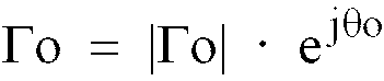
- Since the mounted point Pda of the probe PR1 is apart by a distance of λg/2 in the longitudinal direction of the
rectangular waveguide 13 from the reference point Ps₁ at which the stub S1 is mounted, the reflection coefficient Γo expressed by the above equation (3) is a reflection coefficient at the reference point Ps₁. - As shown in Fig. 6, respective vectors


- Furthermore, as is apparent from Fig. 6, the squares of respective amplitudes of the voltage standing wave |Va|, |Vb| and |Vc| detected by the probes PR1, PR2 and PR3 are expressed as follows:


- Furthermore, the absolute value |Γo| of the reflection coefficient Γ=o is expressed as follows:

- Therefore, since respective amplitudes |Va|, |Vb| and |Vc| of the voltage standing wave can be measured by the voltage
standing wave detector 31, the absolute value |Γo| and the phase θo of the reflection coefficient Γo can be obtained by calculating the solutions of the simultaneous equations (4) to (7). Furthermore, the admittance or the impedance seen looking toward theplasma generating apparatus 30 at the reference point Ps₁ can be calculated using equations (9) to (11) which are described later, from the absolute value |Γo| and the phase θo. - The triple-
stub tuner 32 comprises three stubs S1, S2 and S3 mounted at respective points Ps₁, Ps₂ and Ps₃ of therectangular waveguide 13 at equal spaces of λg/4 in the longitudinal direction thereof, as described above. - Fig. 21 shows a relationship between an insertion length L of each of the stubs S1, S2 and S3 when inserted into the
rectangular waveguide 13, and a susceptance B connected to the mounted point of each stub in therectangular waveguide 13. - As is apparent from Fig. 21, as the insertion length L of each of the stubs S1, S2 and S3 increases, the susceptance B of the mounted point increases. Namely, each of the stubs S1, S2 and S3 operates as an admittance element having a pure susceptance B.
- Fig. 7 shows an equivalent circuit of the triple-
stub tuner 32 which is connected between themicrowave oscillator 10 and theplasma generating apparatus 30. - Referring to Fig. 7, the
microwave oscillator 10, respective admittance elements Ys₁, Ys₂ and Ys₃ of the stubs S1, S2 and S3, and a load admittance Yℓ of the plasma generating apparatus are connected in parallel. Therefore, the triple-stub tuner 32 can adjust the admittance Yo = Go + jBo seen looking toward the load of theplasma generating apparatus 30 at the reference point Ps₁ where the stub S1 is mounted, to a desirable admittance Ys = 1/Zs. - For example, in order to match the load admittance Yo seen looking toward the
plasma generating apparatus 30 to the admittance of themicrowave oscillator 10, it is apparent that the stubs S1, S2 and S3 are respectively inserted into therectangular waveguide 13 by such insertion lengths that the admittance Yo seen looking toward theplasma generating apparatus 30 at the reference point Ps₁ is matched to the admittance Yso = 1/Zso seen looking toward themicrowave oscillator 10 at the reference point Ps₁. - In the automatic microwave impedance adjusting apparatus of the present preferred embodiment, there is calculated the insertion lengths of respective stubs S1, S2 and S3 required for adjusting the admittance Yo seen looking toward the load of the
plasma generating apparatus 30 at the reference point Ps₁ to a desirable admittance Ys including the admittance Yso seen looking toward themicrowave oscillator 10 at the reference point Ps₁, by theCPU 60 of thecontroller 50, and then, the stepping motors M1, M2 and M3 are driven so that the stubs S1, S2 and S3 are inserted into therectangular waveguide 13 by the calculated insertion lengths, respectively. - Fig. 8 shows a relationship between a Smith chart and a UV orthogonal coordinates (referred to as a UV coordinates hereinafter) of a complex plane of a reflection coefficient Γ.
- As shown in Fig. 8, the reflection coefficient Γo at the reference point Ps₁ is expressed as follows:

- where uo and vo are a coordinate value of the U-axis and a coordinate value of the V-axis of the UV coordinates.
- Furthermore, the admittance Yo = 1/Zo seen looking toward the load of the
plasma generating apparatus 30 at the reference point Ps₁ is uniquely expressed as follows:
- An admittance point Pp of the admittance Yo is shown on the Smith chart and the UV coordinates of Fig. 8. Furthermore, the conductance Go and the susceptance bo of the admittance Yo are uniquely expressed as follows:


- Furthermore, transforming the above equations (8) and (9) gives:


- The above equation (12) represents a G = Go circle which includes the admittance point Pp on the Smith chart and is tangent to a U = -1 straight line, as shown in Fig. 8. Also, the above equation (13) represents a B = Bo circle which includes the admittance point Pp on the Smith chart and a point of the UV coordinates (-1, j0)uv, as shown in Fig. 8.
- It is to be noted that, in the specification and Figs. 8 to 20, UV coordinates of an admittance point located on the Smith chart are represented hereinafter by a coordinate representation with a suffix "uv" such as (0, j)uv, (1, j0)uv, and also, coordinates of an admittance point located on the Smith chart which indicate a conductance and a susceptance thereof is represented hereinafter by a coordinate representation without any suffix such as (Go, jBo).
- When the insertion length of the stub S1 located at the reference point Ps₁ or the stub S3 located at the point Ps₃ apart from the reference point Ps₁ by a distance of λg/2 in the longitudinal direction of the
rectangular waveguide 13 is changed, only the susceptance B to be connected to the point Ps₁ at Ps₃ of therectangular waveguide 13 changes, as described above. Therefore, when the insertion length of the stub S1 or S3 of the triple-stub tuner 32 is changed, the admittance point Pp of the admittance Yo seen looking toward the load of theplasma generating apparatus 30 at the points Ps₁ and Ps₃ moves on the G = Go circle on the Smith chart shown in Fig. 8. - Furthermore, an admittance point of an admittance Yo' seen looking toward the load of the
plasma generating apparatus 30 at the point Ps₂ of the stub S2 is located at a point Pp' given when the admittance point Pp of the admittance Yo on the Smith chart is-rotated around the original O of the UV coordinates by 180 degrees, and the admittance Yo' is uniquely expressed as follows:
- It is to be noted that respective references of an admittance, a conductance and a susceptance seen looking toward the load of the
plasma generating apparatus 30 are suffixed with a dash mark ' so as to distinguish them from those seen looking toward the load at the reference point Ps₁. - Further, the conductance Go' and the susceptance Bo' of the admittance Yo' are uniquely expressed as follows:


- Furthermore, transforming the above equations (15) and (16) gives:


- The above equation (17) represents a G' = Go' circle which includes the admittance point Pp' on the Smith chart and is tangent to a U = 1 straight line, as shown in Fig. 9, and the G' = Go' circle and the G = Go circle are point symmetric with respective to the origin O of the UV coordinates. Also, the above equation (18) represents a B' = Bo' circle which includes the admittance point Pp' on the Smith chart and a point of the UV coordinates (1, j0)uv, as shown in Fig. 8, and the B' = Bo' circle and the B = Bo circle are point symmetric with respective to the origin O of the UV coordinates.
- It is to be noted that, in Figs. 9 to 20, the coordinates of the Smith chart are represented by coordinates of an admittance point of an admittance seen looking toward the load at the reference point Ps₁. Furthermore, in all Figs. 9 to 20, a G = G' = ∞ circle which includes points of the UV coordinates (1, j0)uv, (0, j)uv, (-1, j0)uv and (0, -j)uv is drawn as a maximum reference circle.
- When the insertion length of the stub S2 located at the point Ps₂ of the
rectangular waveguide 13 is changed, only the susceptance B to be connected to the point Ps₂ of therectangular waveguide 13 changes, as described above. Therefore, when the insertion length of the stub S2 of the triple-stub tuner 32 is changed, the admittance point Pp' of the admittance Yo' seen looking toward the load of theplasma generating apparatus 30 at the points Ps₂ moves on the G' = Go' circle on the Smith chart shown in Fig. 9. - In the impedance adjusting process executed by the
CPU 60 of thecontroller 50 as described later, the susceptance Bo' of the admittance Yo' seen looking toward the load at the point Ps₂ of the stub S2 is calculated from the UV coordinates of the admittance point Po of the admittance Yo seen looking toward the load at the reference point Ps₁, and also, the susceptance Bo of the admittance Yo seen looking toward the load at the reference point Ps₁ is calculated from the UV coordinates of the admittance point Pp' of the admittance Yo' seen looking toward the load at the point Ps₂ of the stub S2. In these calculations, the converted susceptance can be calculated by inverting respective signs of the coordinate values of the U-axis and V-axis and substituting the inverted UV coordinates into the equation (11). - Fig. 22 is flowchart showing a main routine of an impedance adjusting process executed by the
CPU 60 of thecontroller 50. The main routine includes two subroutines executed atsteps # 7 and #8 of Fig. 22. - Referring to Fig. 22, first of all, at
step # 1, either the repeat operation mode or the single operation mode is selected using the operation mode selection key of thekeyboard 72, and then, atstep # 2, an absolute value |Γs| and a phase θs of a desirable reflection coefficient Γs corresponding to a desirable impedance Zs seen looking toward the load at the reference point Ps₁ are inputted using a set of ten keys of thekeyboard 72. - Thereafter, at
step # 3, theCPU 60 calculates a conductance Gs and a susceptance Bs of a desirable admittance Ys corresponding to the inputted reflection coefficient Γs, using the equations (9) to (11) from the absolute value |Γs| and the phase θo which have been inputted, wherein the admittance point of the desirable admittance Ys is located at an intersection Ps of the G = Gs circle and the B = Bs circle on the Smith chart, as shown in Fig. 10. Thereafter, there are calculated a conductance Gs' and a susceptance Bs' of an admittance Ys' seen looking toward the load at the point Ps₂ of the stub S2 which is given when the phase of the admittance Ys is inverted, using the equations (15) and (16). - Furthermore, at
step # 4, there are calculated the amplitudes of the voltage standing wave |Va|, |Vb| and |Vc| from respective voltages detected by the diodes DI1, DI2 and DI3 which are respectively connected to the probes PR1, PR2 and PR3 of the voltagestanding wave detector 31, and then, atstep # 5, there are calculated the absolute value |Γo| and the phase θo of the reflection coefficient Γo at the reference point Ps₁ by calculating the solutions of the simultaneous equations (4) to (7). It is to be noted that the admittance point of the admittance (referred to as a reference admittance hereinafter) Yo corresponding to the calculated reflection coefficient Γo at the reference point Ps₁ is located at an intersection Po of the G = Go circle and the B = Bo circle on the Smith chart, as shown in Fig. 11. - Thereafter, at
step # 6, it is judged whether the admittance point Po of the reference admittance Yo detected by the voltagestanding wave detector 31 is located within a tuning region Rx₁ shown in Fig. 12, or a tuning region Ry₁ shown in Fig. 15. Then, if the admittance point Po is located within the tuning region Rx₁, the program flow goes to step #7, and then, the impedance adjusting process using the stubs S2 and S3 is executed so as to adjust the reference admittance Yo to the above desirable admittance Ys, and the program flow goes to step #9. On the other hand, if the admittance point Po is located within the tuning region Ry₁, the program flow goes to step #8, and then, the impedance adjusting process using the stubs S1 and S2 is executed so as to adjust the reference admittance Yo to the above desirable admittance Ys, and the program flow goes to step #9. - As shown in Fig. 12, the tuning region Rx₁ is a region located within the G = G' = ∞, and is composed of a sum of:
- (a) a region located within a G' = Gs' circle which includes the admittance point Ps of the admittance Ys on the Smith chart, and is tangent to the U = 1 straight line; and
- (b) a region of all the positive coordinate of the V-axis of the UV coordinates given excluding a region located within a G = Gs circle which includes the admittance point Ps and is tangent to the U = -1 straight line. If the admittance point Po of the reference admittance Yo on the Smith chart is located in the tuning region Rx₁, the reference admittance Yo can be adjusted to the desirable admittance Ys using two stubs S2 and S3.
- Furthermore, as shown in Fig. 15, the tuning region Ry₁ is a region located within the G = G' = ∞ given excluding the tuning region Rx₁. If the admittance point Po of the reference admittance Yo is located in the tuning region Ry₁ on the Smith chart the reference admittance Yo can be adjusted to the desirable admittance Ys using two stubs S1 and S1.
- It is to be noted that, if the admittance point Po is located on the G = Gs circle of a boundary line between the tuning regions Rx₁ and Ry₁, the above impedance adjusting process can be executed using only either stub S1 or S3. On the other hand, if the admittance point Po is located on the G' = Gs' circle of a boundary line between the tuning regions Rx₁ and Ry₁, the above impedance adjusting process can be executed using only the stub S2.
- Furthermore, at
step # 9, it is judged whether or not the operation mode is set at the repeat operation mode. If the operation mode is set at the repeat operation mode, the program flow goes to step #4, and then, the processes fromsteps # 4 are repeated. On the other hand, if the operation mode is set at the single operation mode, the impedance adjusting mode is completed. - The repeat operation mode is useful for adjusting the impedance seen looking toward the load having a load impedance changing with a time such as the
plasma generating apparatus 30. Namely, at a time t0, there is calculated reflection coefficient ro corresponding to the reference admittance Yo in the processes ofsteps # 4 and #5. However, if the load impedance at a time t1 defined after the time t0 is shifted from the load impedance at the time t0, the reference admittance Yo after executing the impedance adjusting process atstep # 7 or #8 is mismatched to the desirable admittance Ys corresponding to the desirable reflection coefficient rs which has been previously inputted atstep # 2. If the repeat operation mode is set in the automatic microwave impedance adjusting apparatus, the automatic microwave impedance adjusting apparatus has such an advantage that the impedance adjusting process can be executed depending on a change in the load impedance of the load such as theplasma generating apparatus 30, even though the load impedance changes. - In order to match the impedance seen looking toward the
microwave oscillator 10 to the impedance seen looking toward the load of theplasma generating apparatus 30, atstep # 2, "zero" and "any number" are inputted as the absolute value |Γs| and the phase θs of the reflection coefficient Γs, respectively. - Furthermore, in the case of the load of the
plasma generating apparatus 30, the reference impedance seen looking toward the load may not become a certain desirable impedance stably due to a frequent change in the load impedance of theplasma generating apparatus 30, even though the impedance adjusting process of the present preferred embodiment is executed so that the reference impedance seen looking toward the load at the reference point Ps₁ is matched to the impedance seen toward themicrowave oscillator 10. In this case, atstep # 2, there are inputted an absolute value |Γs| and a phase θs of a desirable reflection coefficient Γs close to the impedance matching point located at the origin O of the UV coordinates so as to adjust the above reference admittance Yo to a desirable admittance Ys corresponding the above inputted reflection coefficient Γs, resulting in a stable reference impedance seen looking toward the load at the reference point Ps₁. - Fig. 23 is a flowchart showing the subroutine of the impedance adjusting process using the stubs S2 and S3 (
step # 7 of Fig. 22). - Referring to Fig. 23, first of all, at
step # 11, there is calculated a susceptance Bo seen looking toward the load at the reference point Ps₁ using the equations (8) and (11) from the absolute value |Γo| and the phase θo of the reflection coefficient Γo at the reference point Ps₁ which have been calculated atstep # 5, and then, atstep # 12, there are calculated the UV coordinates of an intersection Pa of the G = Go circle and the G' = Gs' circle shown in Fig. 13, using the equation (12) and (17). - Thereafter, at
step # 13, there is calculated a susceptance Ba of the intersection Pa from the UV coordinates of the intersection Pa, and then, atstep # 14, there is calculated a susceptance B₃₀ to be connected by the stub S3 to the transmission line of therectangular waveguide 13, which is expressed by the following equation (19) :
- The susceptance B₃₀ is a difference between respective susceptances of the admittance points Po and Pa which are located on the G = Go circle on the Smith chart shown in Fig. 13.
- Thereafter, at
step # 15, there is calculated a susceptance Ba' seen looking toward the load at the point Ps₂ of the stub S2 using the equation (11), as described above, from the UV coordinates of the above susceptance Ba. - Thereafter, at
step # 16, there is calculated a susceptance B₂₀' to be connected by the stub S2 to the transmission line of therectangular waveguide 13, which is expressed by the following equation (20):
- The susceptance B₂₀' is a difference between respective susceptances of the admittance points Ps and Pa which are located on the G' = Gs' circle on the Smith chart shown in Fig. 14.
- Thereafter, at
step # 17, there are calculated insertion lengths of the stubs S2 and S3 using the relationship between the insertion length L thereof and the susceptance B shown in Fig. 21 which has been previously measured, from the calculated susceptances B₂₀' and B₃₀, and then, atstep # 18, the stepping motors M2 and M3 are driven, respectively, so that the stubs S2 and S3 are inserted into therectangular waveguide 13 by the calculated insertion lengths. Then, the reference admittance Yo is adjusted to the desirable admittance Ys. - Fig. 24 is a flowchart showing the subroutine of the impedance adjusting process using the stubs S1 and S2 (
step # 8 of Fig. 22). - Referring to Fig. 24, first of all, at
step # 21, there is calculated a susceptance Bo' seen looking toward the load at the point Ps₂ using the equations (15) and (16) from the absolute value |Γo| and the phase θo of the reflection coefficient Γo at the reference point Ps₁ which have been calculated atstep # 5, and then, atstep # 22, there are calculated the UV coordinates of an intersection Pb of the G' = Go' circle and the G = Gs circle shown in Fig. 16, using the equation (12) and (17). - Thereafter, at
step # 23, there is calculated a susceptance Bb' of the intersection Pb from the UV coordinates of the intersection Pb, and then, atstep # 24, there is calculated a susceptance B₂₀' to be connected by the stub S2 to the transmission line of therectangular waveguide 13, which is expressed by the following equation (21):
- The susceptance B₂₀' is a difference between respective susceptances of the admittance points Po and Pb which are located on the G' = Go' circle on the Smith chart shown in Fig. 16.
- Thereafter, at
step # 25, there is calculated a susceptance Bb seen looking toward the load at the reference point Ps₁ using the equation (11), as described above, from the UV coordinates of the above susceptance Bb'. - Thereafter, at
step # 26, there is calculated a susceptance B₁₀ to be connected by the stub S1 to the transmission line of therectangular waveguide 13, which is expressed by the following equation (22):
- The susceptance B₁₀ is a difference between respective susceptances of the admittance points Ps and Pb which are located on the G = Gs circle on the Smith chart shown in Fig. 17.
- Thereafter, at
step # 27, there are calculated insertion lengths of the stubs S1 and S2 using the relationship between the insertion length L thereof and the susceptance B shown in Fig. 21 which has been previously measured, from the calculated susceptances B₁₀ and B₂₀', and then, atstep # 28, the stepping motors M1 and M2 are driven, respectively, so that the stubs S1 and S2 are inserted into therectangular waveguide 13 by the calculated insertion lengths. Then, the reference admittance Yo is adjusted to the desirable admittance Ys. - Figs. 18 and 19 are Smith charts and complex planes of UV coordinates showing tuning regions Rx₀ and Ry₀ corresponding to the tuning regions Rx₁ and Ry₁, in the case of an impedance matching process for matching the reference admittance Yo seen looking toward the load of the
plasma generating apparatus 30 at the reference point Ps₁ to the admittance Yso = 1/Zso seen looking toward themicrowave oscillator 10 thereat. - In Figs. 18 and 19, the tuning region Rx₀ is a region where the impedance matching process is executed using the stubs S2 and S3 when the admittance point Po of the reference admittance Yo is located within the tuning region Rx₀ on the Smith chart, and the tuning region Ry₀ is a region where the impedance matching process is executed using the stubs S1 and S2 when the admittance point Po of the reference admittance Yo is located within the tuning region Ry₀ on the Smith chart.
- As shown in Figs. 18 and 19, the admittance point Ps of the desirable admittance Ys becomes the origin Pso of the UV coordinates, and a boundary line between the tuning regions Rx₀ and Ry₀ is composed of half the G = 1 circle for any positive coordinate value of the V-axis of the UV coordinates, and half the G' = 1 circle for any negative coordinate value of the V-axis of the UV coordinates.
- The impedance matching process shown in Fig. 18 is executed in a manner similar to that of the subroutine of
step # 7, and the impedance matching process shown in Fig. 19 is executed in a manner similar to that of the subroutine ofstep # 8. - At
step # 6 of the present preferred embodiment, it is judged whether the admittance point Po of the reference admittance Yo is located within the tuning region Rx₁ or Ry₁, and then, the impedance adjusting process using the stubs S2 and S3 is executed if the point Po is located within the tuning region Rx₁, on the other hand, the impedance adjusting process using the stubs S1 and S2 is executed if the point Po is located within the tuning region Ry₁. However, the present invention is not limited to this. If the admittance point Po is located at a partial region (referred to as a tuning region Rz₁ hereinafter) of the tuning region Ry₁ for any positive coordinate value of the V-axis of the UV coordinates, an impedance adjusting process may be executed using all the stubs S1, S2 and S3. Then, the reference admittance Yo can be adjusted to a desirable admittance Ys, for a time shorter than that of the impedance adjusting process using the stubs S1 and S2, in the above case. - Fig. 18 is a Smith chart and a complex plane of a UV coordinates showing an operation of an impedance matching process using all the stubs S1, S2 and S3.
- If the admittance point Po of the reference admittance Yo is located within a tuning region Rz₀ on the Smith chart shown in Fig. 18, the impedance matching process is executed using all the stubs S1, S2 and S3, wherein the tuning region Rz₀ is a region located within half the G = 1 for any positive value of the V-axis of the UV coordinates.
- In the impedance matching process, as shown in the Smith chart of Fig. 20, the admittance point Po of the reference admittance Yo is moved using the stub S3 to an intersection Pa of the G = Go circle and the U-axis, and then, the admittance point Pa is moved using the stub S2 to an intersection Pb of the G = 1 circle and a G' = Ga', wherein the G' = Ga' circle includes the admittance point Pa and is tangent to the U = 1 straight line. Thereafter, the admittance point Pb is moved using the stub S1 to the impedance matching point Pso. Thus, the susceptances of respective stubs S1, S2 and S3 are changed so as to match the reference admittance Yo to the admittance Yso seen looking toward the
microwave oscillator 10 at the reference points Ps₁. the calculation of this impedance matching process is executed in a manner similar to that of the subroutine ofstep # 7 or #8. - In the present preferred embodiment, there are calculated the absolute value |Γo| and the phase θo of the reflection coefficient |Γo| at the reference point by the
CPU 60 from the amplitudes of the voltage standing wave detected by respective probes PR1, PR2 and PR3 by the standing wave measuring method using the probes PR1, PR2 and PR3 and the diodes DI1, DI2 and DI3. However, the present invention is not limited to this. For example, after measuring the impedance seen looking to a load at a point of a microwave transmission line by another measuring method for measuring the impedance thereof, a reflection coefficient corresponding to the measured impedance may be calculated, and then, the impedance adjusting process of the present invention may be executed. - In the voltage
standing wave detector 31 of the present preferred embodiment, three probes PR1, PR2 and PR3 are mounted at equal spaces of λg/6 in the longitudinal direction of therectangular waveguide 13. However, the present invention is not limited to this. At least three probes may be mounted at different points at predetermined spaces, one of which is not a product of any natural number and the length λg/2. Each space between the probes is preferably set at a length equal to a product of any natural number and the length λg/6 except for products of any natural number and the length λg/2. For example, when each space between the probes is set at the length λg/3, the squares of the amplitudes of the voltage standing wave detected by respective probes PR1, PR2 and PR3 are expressed as follows:


- In the present preferred embodiment, the space in the longitudinal direction of the
rectangular waveguide 13 between the stub S1 and the probe PR1 is set at the length λg/2 for convenience of the explanation. However, the present invention is not limited to this. This space may be set at any distance. - At
step # 2 of Fig. 22 of the present preferred embodiment, there are inputted the absolute value |Γs| and the phase θo of the reflection coefficient Γs corresponding to the desirable impedance Zs seen looking toward the load at the reference point Ps₁. However, the present invention is not limited to this. A resistance Rs and a reactance Xs of a desirable impedance Zs may be in putted, or a conductance Gs and a susceptance Bs of a desirable admittance Ys corresponding to a desirable impedance Zs may be inputted.
Claims (4)
- An automatic microwave impedance adjusting method including a first step of measuring either an impedance seen looking towards a microwave load (3) at a predetermined reference point of a microwave transmission line of a rectangular waveguide (13) connected between a microwave oscillator (10) and said microwave load (30) or a reflection coefficient thereat by detecting a voltage standing wave of a microwave propagating on said microwave transmission line;wherein said method includes:a second step of calculating insertion lengths of first to third stubs (S1, S2 and S3) of variable impedance means so as to adjust said impedance seen looking towards said microwave load (30) to a desired value corresponding to an inputted desired reflection coefficient, responsive to said value measured at said first step, said first to third stubs (S1, S2 and S3) being mounted on said microwave load side of said reference point on said microwave transmission line, and mounted at different points in an order of said first to third stubs (S1, S2 and S3) at equal spaces of a quarter of said waveguide length in the longitudinal direction of said rectangular waveguide (13), anda third step of inserting said first to third stubs (S1, S2 and S3) into said rectangular waveguide (13) by insertion lengths calculated at said second step, thereby adjusting said impedance seen looking towards said microwave load (30) to said desired value,characterised in that a whole region within a Smith chart representing an impedance seen looking towards said microwave load (30) is divided into a first region (Ry) for executing said impedance adjusting process of said third step using first and second stubs (S1, S2) when an impedance point seen looking towards said microwave load (30) at said reference point is located within said first region (Ry), a second region (Rx) for executing said impedance adjusting process of said third step using said second and third stubs (S2, S3) when said impedance point is located within said second region (Rx), and a third region (Rz) for executing said impedance adjusting of said third step using all said first to third stubs (S1, S2 and S3) when said impedance point is located within said third region (Rz), said third region (Rz) being defined as a partial region of said first region (Ry) for any positive coordinate value of a V-axis of a UV orthogonal coordinate of the Smith chart; andwherein said second step includes:calculating an impedance seen looking towards said microwave load (30) at said reference point responsive to said value measured at said first step; andjudging whether an impedance point of said calculated impedance is located within either said first region (Ry), said second region (Rx) or said third region (Rz) on said Smith chart; andwherein said third step includes:executing said impedance adjusting process of said third step using said first and second stubs (S1, S2) when it is judged that said impedance point of said calculated impedance is located within said first region (Ry), executing said impedance adjusting process of said third step using said second and third stubs (S2, S3) when it is judged that said impedance point of said calculated impedance is located within said second region (Rx), and executing said impedance adjusting process of said third step using all said first to third stubs (S1, S2 and S3) when it is judged that said impedance point of said calculated impedance is located within said third region (Rz).
- A method as claimed in claim 1, wherein a whole region within a Smith chart representing an impedance seen looking towards said microwave load (30) is divided into a first region for executing said impedance adjusting process of said third step using said first and second stubs (S1, S2) when an impedance point seen looking towards said microwave load (30) at said reference point is located within said first region, and a second region for executing said impedance adjusting process of said third step using said second and third stubs (S2, S3) when said impedance point is located within said second region;wherein said second step includes:calculating an impedance seen looking towards said microwave load (30) at said reference point responsive to said value measured at said first step, andjudging whether an impedance point of said calculated impedance is located within either said first region or said second region of said Smith chart, andwherein said third step includes:executing said impedance adjusting process of said third step using said first and second stubs (S1, S2) when it is judged that said impedance point of said calculated impedance is located within said first region, and executing said impedance adjusting process of said third step using said second and third stubs (S2, S3) when it is judged that said impedance point of said calculated impedance is located within said second region.
- A method as claimed in any one of claims 1 and 2, wherein said processes of said first to third steps are repeated.
- An automatic microwave impedance adjusting apparatus for performing the method of any one of claims 1 to 3 and comprising:a microwave transmission line connected between a microwave oscillator (10) and a microwave load (3), said microwave transmission line being a rectangular waveguide (13),measuring means for measuring either an impedance seen looking towards said microwave load (30) at a mounted point thereof or a reflection coefficient thereat by detecting a voltage standing wave of a microwave propagating on said microwave transmission line,variable impedance means (32) for changing an impedance to be connected to a mounted point thereof, andcontrol means (5) for controlling said variable impedance means (32) responsive to a value measured by said measuring means so as to adjust said impedance to a desired value corresponding to an inputted desired reflection coefficient,characterised in thatsaid variable impedance means (32) are mounted on said microwave load side of said measuring means on said microwave transmission line, said variable impedance means (32) comprising three stubs (S1, S2 and S3) mounted at different points at equal spaces of a quarter of said waveguide wavelength in the longitudinal direction of said rectangular waveguide (13), andsaid control means (5) comprises:calculating means for calculating insertion lengths of first to third stubs (S1, S2 and S3) of variable impedance means so as to adjust said impedance seen looking towards said microwave load (30) to a desired value corresponding to an inputted desired reflection coefficient, responsive to said value measured by said measuring means, andinsertion control means for inserting said first to third stubs (S1, S2 and S3) into said rectangular waveguide (13) by insertion lengths calculated by said calculating means, thereby adjusting said impedance seen looking towards said microwave load (30) to said desired value,wherein a whole region within a Smith chart representing an impedance seen looking towards said microwave load (30) is divided into a first region (Ry) for executing said impedance adjusting process of said insertion control means using first and second stubs (S1, S2) when an impedance point seen looking towards said microwave load (30) at said reference point is located within said first region (Ry), a second region (Rx) for executing said impedance adjusting process of said insertion control means using said second and third stubs (S2, S3) when said impedance point is located within said second region (Rx), and a third region (Rz) for executing said impedance adjusting of said insertion control means using all said first to third stubs (S1, S2 and S3) when said impedance point is located within said third region (Rz), said third region (Rz) being defined as a partial region of said first region (Ry) for any positive coordinate value of a V-axis of a UV orthogonal coordinate of the Smith chart; andwherein said calculating means comprises:means for calculating an impedance seen looking towards said microwave load (30) at said reference point responsive to said value measured by said measuring means; andmeans for judging whether an impedance point of said calculated impedance is located within either said first region (Ry), said second region (Rx) or said third region (Rz) on said Smith chart; andwherein said insertion control means comprises:executing said impedance adjusting process of said insertion control means using said first and second stubs (S1, S2) when it is judged that said impedance point of said calculated impedance is located within said first region (Ry), executing said impedance adjusting process of said insertion control means using said second and third stubs (S2, S3) when it is judged that said impedance point of said calculated impedance is located within said second region (Rx), and executing said impedance adjusting process of said insertion control means using all said first to third stubs (S1, S2 and S3) when it is judged that said impedance point of said calculated impedance is located within said third region (Rz).
Applications Claiming Priority (6)
| Application Number | Priority Date | Filing Date | Title |
|---|---|---|---|
| JP22038/89 | 1989-01-30 | ||
| JP2203889 | 1989-01-30 | ||
| JP251684/89 | 1989-09-26 | ||
| JP25168489 | 1989-09-26 | ||
| JP14457/90 | 1990-01-24 | ||
| JP2014457A JP2986166B2 (en) | 1989-01-30 | 1990-01-24 | Apparatus and method for automatically adjusting impedance of microwave circuit |
Publications (3)
| Publication Number | Publication Date |
|---|---|
| EP0381398A2 EP0381398A2 (en) | 1990-08-08 |
| EP0381398A3 EP0381398A3 (en) | 1991-07-10 |
| EP0381398B1 true EP0381398B1 (en) | 1996-01-03 |
Family
ID=27280646
Family Applications (1)
| Application Number | Title | Priority Date | Filing Date |
|---|---|---|---|
| EP19900300870 Expired - Lifetime EP0381398B1 (en) | 1989-01-30 | 1990-01-29 | Automatic impedance adjusting apparatus for microwave load and automatic impedance adjusting method therefor |
Country Status (2)
| Country | Link |
|---|---|
| EP (1) | EP0381398B1 (en) |
| DE (1) | DE69024509T2 (en) |
Families Citing this family (10)
| Publication number | Priority date | Publication date | Assignee | Title |
|---|---|---|---|---|
| JP2981284B2 (en) * | 1990-11-28 | 1999-11-22 | 株式会社ダイヘン | Power supply for microwave oscillator |
| DE4135555C2 (en) * | 1991-10-29 | 1993-10-07 | Ant Nachrichtentech | Method for determining the output reflection factor and the backward transmission factor of a measurement object and use of the method |
| US6297649B1 (en) | 1999-09-30 | 2001-10-02 | Focus Microwaves Inc. | Harmonic rejection load tuner |
| US20050185769A1 (en) * | 2004-02-25 | 2005-08-25 | Pickerd John J. | Calibration method and apparatus |
| DE102005005887A1 (en) * | 2005-02-09 | 2006-08-10 | Rohde & Schwarz Gmbh & Co. Kg | Method and arrangement for correcting the retroactivity of electrical transducers on the object to be measured |
| US7460983B2 (en) | 2006-08-23 | 2008-12-02 | Tektronix, Inc. | Signal analysis system and calibration method |
| US7405575B2 (en) | 2006-08-23 | 2008-07-29 | Tektronix, Inc. | Signal analysis system and calibration method for measuring the impedance of a device under test |
| US7408363B2 (en) | 2006-08-23 | 2008-08-05 | Tektronix, Inc. | Signal analysis system and calibration method for processing acquires signal samples with an arbitrary load |
| US7414411B2 (en) | 2006-08-23 | 2008-08-19 | Tektronix, Inc. | Signal analysis system and calibration method for multiple signal probes |
| CN116192170B (en) * | 2022-12-30 | 2025-11-14 | 中国电信股份有限公司 | A method, apparatus, electronic device, and storage medium for adjusting the impedance of a transmission line. |
Family Cites Families (5)
| Publication number | Priority date | Publication date | Assignee | Title |
|---|---|---|---|---|
| US3617953A (en) * | 1971-03-16 | 1971-11-02 | Canadian Patents Dev | Microwave impedance matching system |
| GB1400895A (en) * | 1973-06-27 | 1975-07-16 | Canadian Patents Dev | Microwave heating apparatus |
| GB2100526B (en) * | 1981-05-21 | 1985-04-24 | Secr Defence | Improvements in or relating to impedance matching devices |
| US4679007A (en) * | 1985-05-20 | 1987-07-07 | Advanced Energy, Inc. | Matching circuit for delivering radio frequency electromagnetic energy to a variable impedance load |
| US4965607A (en) * | 1987-04-30 | 1990-10-23 | Br Communications, Inc. | Antenna coupler |
-
1990
- 1990-01-29 EP EP19900300870 patent/EP0381398B1/en not_active Expired - Lifetime
- 1990-01-29 DE DE1990624509 patent/DE69024509T2/en not_active Expired - Lifetime
Also Published As
| Publication number | Publication date |
|---|---|
| DE69024509D1 (en) | 1996-02-15 |
| EP0381398A2 (en) | 1990-08-08 |
| DE69024509T2 (en) | 1996-06-13 |
| EP0381398A3 (en) | 1991-07-10 |
Similar Documents
| Publication | Publication Date | Title |
|---|---|---|
| US5079507A (en) | Automatic impedance adjusting apparatus for microwave load and automatic impedance adjusting method therefor | |
| US5621331A (en) | Automatic impedance matching apparatus and method | |
| EP0381398A2 (en) | Automatic impedance adjusting apparatus for microwave load and automatic impedance adjusting method therefor | |
| KR100775881B1 (en) | Plasma processing device and controlling method therefor | |
| EP0552955A1 (en) | Electronically tuned matching network using predictor-corrector control system | |
| US5053725A (en) | Circuit configuration for the automatic tuning of a matching network | |
| Wexler | Solution of waveguide discontinuities by modal analysis | |
| EP0731559A1 (en) | RF plasma power supply combining technique for increased stability | |
| US7642879B2 (en) | Impedance matching apparatus | |
| KR0170400B1 (en) | Vacuum processing device with automatic calibration of pressure gauge output | |
| Ying | General Takagi-Sugeno fuzzy systems are universal approximators | |
| US5041803A (en) | Automatic load matching circuit for microwaves using multi-element matching device | |
| KR20150039725A (en) | Impedance Matching Method And Impedance Matching System | |
| US5926385A (en) | Feedback control method for chaos system using adaptive tracking | |
| EP0575671A1 (en) | Microwave power source apparatus for microwave oscillator comprising means for automatically adjusting transmitted wave power and control method therefor | |
| Schuster et al. | New method for determining the largest Liapunov exponent of simple nonlinear systems | |
| JP3021093B2 (en) | Plasma impedance measuring device | |
| JP3670188B2 (en) | Impedance matching device | |
| JPH0375082B2 (en) | ||
| US6215319B1 (en) | High accuracy measuring system | |
| Ghosh et al. | Software based linearisation of thermistor type nonlinearity | |
| Can et al. | Design of the neutrosophic membership valued fuzzy-PID controller and rotation angle control of a permanent magnet direct current motor | |
| JP3107757B2 (en) | Automatic tuning method of microwave circuit | |
| JP3578701B2 (en) | Air pump maximum output control device | |
| KR102429080B1 (en) | Plasma processing device and operating method of plasma processing device |
Legal Events
| Date | Code | Title | Description |
|---|---|---|---|
| PUAI | Public reference made under article 153(3) epc to a published international application that has entered the european phase |
Free format text: ORIGINAL CODE: 0009012 |
|
| AK | Designated contracting states |
Kind code of ref document: A2 Designated state(s): DE FR GB |
|
| 17P | Request for examination filed |
Effective date: 19910207 |
|
| PUAL | Search report despatched |
Free format text: ORIGINAL CODE: 0009013 |
|
| AK | Designated contracting states |
Kind code of ref document: A3 Designated state(s): DE FR GB |
|
| 17Q | First examination report despatched |
Effective date: 19931005 |
|
| GRAA | (expected) grant |
Free format text: ORIGINAL CODE: 0009210 |
|
| AK | Designated contracting states |
Kind code of ref document: B1 Designated state(s): DE FR GB |
|
| REF | Corresponds to: |
Ref document number: 69024509 Country of ref document: DE Date of ref document: 19960215 |
|
| ET | Fr: translation filed | ||
| PLBE | No opposition filed within time limit |
Free format text: ORIGINAL CODE: 0009261 |
|
| STAA | Information on the status of an ep patent application or granted ep patent |
Free format text: STATUS: NO OPPOSITION FILED WITHIN TIME LIMIT |
|
| 26N | No opposition filed | ||
| REG | Reference to a national code |
Ref country code: GB Ref legal event code: IF02 |
|
| PGFP | Annual fee paid to national office [announced via postgrant information from national office to epo] |
Ref country code: DE Payment date: 20090123 Year of fee payment: 20 |
|
| PGFP | Annual fee paid to national office [announced via postgrant information from national office to epo] |
Ref country code: GB Payment date: 20090128 Year of fee payment: 20 |
|
| PGFP | Annual fee paid to national office [announced via postgrant information from national office to epo] |
Ref country code: FR Payment date: 20090113 Year of fee payment: 20 |
|
| REG | Reference to a national code |
Ref country code: GB Ref legal event code: PE20 Expiry date: 20100128 |
|
| PG25 | Lapsed in a contracting state [announced via postgrant information from national office to epo] |
Ref country code: GB Free format text: LAPSE BECAUSE OF EXPIRATION OF PROTECTION Effective date: 20100128 |
|
| PG25 | Lapsed in a contracting state [announced via postgrant information from national office to epo] |
Ref country code: DE Free format text: LAPSE BECAUSE OF EXPIRATION OF PROTECTION Effective date: 20100129 |