EP0381237B1 - Circuit semi-conducteur intégré avec transistors M.O.S. à canaux P et N - Google Patents
Circuit semi-conducteur intégré avec transistors M.O.S. à canaux P et N Download PDFInfo
- Publication number
- EP0381237B1 EP0381237B1 EP90102104A EP90102104A EP0381237B1 EP 0381237 B1 EP0381237 B1 EP 0381237B1 EP 90102104 A EP90102104 A EP 90102104A EP 90102104 A EP90102104 A EP 90102104A EP 0381237 B1 EP0381237 B1 EP 0381237B1
- Authority
- EP
- European Patent Office
- Prior art keywords
- mos transistors
- potential
- region
- well
- source
- Prior art date
- Legal status (The legal status is an assumption and is not a legal conclusion. Google has not performed a legal analysis and makes no representation as to the accuracy of the status listed.)
- Expired - Lifetime
Links
- 239000004065 semiconductor Substances 0.000 title claims description 36
- 239000000758 substrate Substances 0.000 claims description 37
- 230000003071 parasitic effect Effects 0.000 description 32
- 238000009792 diffusion process Methods 0.000 description 13
- 238000000034 method Methods 0.000 description 6
- 239000000969 carrier Substances 0.000 description 4
- 230000010354 integration Effects 0.000 description 3
- 230000001681 protective effect Effects 0.000 description 2
- 230000001960 triggered effect Effects 0.000 description 2
- 230000006378 damage Effects 0.000 description 1
- 230000001747 exhibiting effect Effects 0.000 description 1
- 238000002347 injection Methods 0.000 description 1
- 239000007924 injection Substances 0.000 description 1
- 238000004519 manufacturing process Methods 0.000 description 1
- 230000004048 modification Effects 0.000 description 1
- 238000012986 modification Methods 0.000 description 1
- 230000003449 preventive effect Effects 0.000 description 1
Images

Classifications
-
- H—ELECTRICITY
- H10—SEMICONDUCTOR DEVICES; ELECTRIC SOLID-STATE DEVICES NOT OTHERWISE PROVIDED FOR
- H10D—INORGANIC ELECTRIC SEMICONDUCTOR DEVICES
- H10D84/00—Integrated devices formed in or on semiconductor substrates that comprise only semiconducting layers, e.g. on Si wafers or on GaAs-on-Si wafers
- H10D84/80—Integrated devices formed in or on semiconductor substrates that comprise only semiconducting layers, e.g. on Si wafers or on GaAs-on-Si wafers characterised by the integration of at least one component covered by groups H10D12/00 or H10D30/00, e.g. integration of IGFETs
- H10D84/82—Integrated devices formed in or on semiconductor substrates that comprise only semiconducting layers, e.g. on Si wafers or on GaAs-on-Si wafers characterised by the integration of at least one component covered by groups H10D12/00 or H10D30/00, e.g. integration of IGFETs of only field-effect components
- H10D84/83—Integrated devices formed in or on semiconductor substrates that comprise only semiconducting layers, e.g. on Si wafers or on GaAs-on-Si wafers characterised by the integration of at least one component covered by groups H10D12/00 or H10D30/00, e.g. integration of IGFETs of only field-effect components of only insulated-gate FETs [IGFET]
- H10D84/85—Complementary IGFETs, e.g. CMOS
- H10D84/854—Complementary IGFETs, e.g. CMOS comprising arrangements for preventing bipolar actions between the different IGFET regions, e.g. arrangements for latchup prevention
-
- H—ELECTRICITY
- H10—SEMICONDUCTOR DEVICES; ELECTRIC SOLID-STATE DEVICES NOT OTHERWISE PROVIDED FOR
- H10D—INORGANIC ELECTRIC SEMICONDUCTOR DEVICES
- H10D84/00—Integrated devices formed in or on semiconductor substrates that comprise only semiconducting layers, e.g. on Si wafers or on GaAs-on-Si wafers
- H10D84/01—Manufacture or treatment
- H10D84/0123—Integrating together multiple components covered by H10D12/00 or H10D30/00, e.g. integrating multiple IGBTs
- H10D84/0126—Integrating together multiple components covered by H10D12/00 or H10D30/00, e.g. integrating multiple IGBTs the components including insulated gates, e.g. IGFETs
- H10D84/0165—Integrating together multiple components covered by H10D12/00 or H10D30/00, e.g. integrating multiple IGBTs the components including insulated gates, e.g. IGFETs the components including complementary IGFETs, e.g. CMOS devices
-
- H—ELECTRICITY
- H10—SEMICONDUCTOR DEVICES; ELECTRIC SOLID-STATE DEVICES NOT OTHERWISE PROVIDED FOR
- H10D—INORGANIC ELECTRIC SEMICONDUCTOR DEVICES
- H10D89/00—Aspects of integrated devices not covered by groups H10D84/00 - H10D88/00
- H10D89/60—Integrated devices comprising arrangements for electrical or thermal protection, e.g. protection circuits against electrostatic discharge [ESD]
- H10D89/601—Integrated devices comprising arrangements for electrical or thermal protection, e.g. protection circuits against electrostatic discharge [ESD] for devices having insulated gate electrodes, e.g. for IGFETs or IGBTs
- H10D89/711—Integrated devices comprising arrangements for electrical or thermal protection, e.g. protection circuits against electrostatic discharge [ESD] for devices having insulated gate electrodes, e.g. for IGFETs or IGBTs using bipolar transistors as protective elements
- H10D89/713—Integrated devices comprising arrangements for electrical or thermal protection, e.g. protection circuits against electrostatic discharge [ESD] for devices having insulated gate electrodes, e.g. for IGFETs or IGBTs using bipolar transistors as protective elements including a PNP transistor and a NPN transistor, wherein each of said transistors has its base region coupled to the collector region of the other transistor, e.g. silicon controlled rectifier [SCR] devices
Definitions
- the present invention relates to a semiconductor circuit formed within a semiconductor substrate comprising:-
- EP-A-0 245 515 describes a semiconductor device designed to prevent the injection of minority carriers into a substrate when the potential applied to the device undergoes changes due to noise or the like.
- Latch-up is a particular phenomenon generally induced between CMOS circuits when parasitic transistors formed in parasitic NPN and PNP regions between adjacent transistor elements of the CMOS circuits are triggered and operated as a thyristor.
- the thyristor causes an uncontrollable excess current to continuously flow from a power source terminal to a ground terminal and to destroy the transistor elements.
- the latch-up phenomenon is triggered when a MOS transistor adjacent to the thyristor formed by the parasitic transistors is turned on. At this moment, hot carriers generated around a drain of the MOS transistor flow to a substrate to upset a normal substrate voltage.
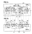
- Figure 1a is a plan view showing a conventional semiconductor circuit for explaining the latch-up phenomenon
- Fig. 1b is a sectional view thereof.
- the conventional semiconductor circuit comprises a P-type substrate 101 on which a low-potential system (Vdd) and a high-potential system (Vpp) are formed adjacent to each other.
- the low-potential system (Vdd) comprises a first P-channel MOS transistor 103 and a first N-channel MOS transistor 105 that are complementarily connected to each other.
- the high-potential system (Vpp) comprises a second P-channel MOS transistor 107 and a second N-channel MOS transistor 109 that are complementarily connected to each other.
- the first N-channel MOS transistor 105 and second P-channel MOS transistor 107 that have different channel polarities are disposed adjacent to each other.
- the first P-channel MOS transistor 103 has a gate electrode 111, a P + drain region 113, a P + source region 115, and an N + region 117 for supplying the Vdd-potential to an N-type well.
- the first N-channel MOS transistor 105 has a gate electrode 119, an N + source region 121, an N + drain region 123, and a P + region 125 for supplying the ground-potential to the P-type substrate 101.
- the second P-channel MOS transistor 107 has a gate electrode 125, P + drain and source regions 127 and 129, and an N + region 131 for supplying the Vpp-potential to the N-type well.
- the second N-channel MOS transistor 109 has a gate electrode 133, N + source and drain regions 135 and 137, and a P + region 139 for supplying the ground-potential to the P-type substrate 101.
- a parasitic NPN transistor 141 and a parasitic PNP transistor 143 are formed.
- CMOS IC complementary metal-oxide-semiconductor
- potentials of the P-type substrate 101 and an N-type well must be kept stably at a ground level and a level of Vpp, respectively.
- the parasitic transistors 141 and 143 act as a thyristor to cause the latch-up phenomenon which causes an uncontrollable excess current to continuously flow from a power source terminal 145 to a grounding terminal 147.
- the instantaneous trigger current flows in an N-type well around the parasitic PNP transistor 143, the potential of the N-type well drops from the level of Vpp to turn on the parasitic PNP transistor 143, thereby turning on the parasitic NPN transistor 141. Then, the parasitic transistors 141 and 143 act as a thyristor to cause the latch-up phenomenon which causes an uncontrollable excess current to continuously flow from the power source terminal 145 to the grounding terminal 147.
- the trigger current may be generated by an internal factor of the chip. At an instance when another MOS transistor in the vicinity of the parasitic transistors 141 and 143 is turned on, hot carriers are thought to be generated around a drain of the MOS transistor and flow to the substrate and N-type well to produce the trigger current.
- the trigger current may also be generated by an external factor of the ship.
- a MOS IC chip has a pad directly connected to a protective diode to prevent electrostatic destruction from the outside of the chip.
- the protective diode When a voltage exceeding a power source voltage is applied to the pad, the protective diode is turned on to free excessive charges to a substrate or to an N-type well. The freed charges are considered to produce the trigger current of the latch-up phenomenon.
- the trigger current generating tendency will be considered for three kinds of power sources, i.e., a grounding, a 5-volt power source Vdd, and a 12.5-volt power source Vpp.
- a known technique of preventing the latch-up phenomenon is to provide a diffusion layer between, for example, a transistor of the Vdd system and a transistor of the Vpp system, to absorb the trigger current.
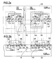
- Figure 2 shows a concrete example of the latch-up preventing technique. This example arranges a diffusion layer as a guard ring for the semiconductor circuit of Fig. 1.
- a P-type diffusion layer 151 is disposed as guard rings along a boundary between the first N-channel MOS transistor 105 of the low-potential system (Vdd) and the second P-channel MOS transistor 107 of the high-potential system (Vpp).
- an N-type diffusion layer 153 is disposed as a guard ring around the N-type well of the second P-channel MOS transistor 107.
- the diffusion layers 151 and 153 prevent the latch-up phenomenon.
- Other arrangement of Fig. 2 is the same as the arrangement of Fig. 1, and therefore, like elements are represented with like reference marks to omit their explanations.
- the diffusion layers however, enlarge a distance between the first N-channel MOS transistor 105 and the second P-channel MOS transistor 107, thereby increasing a chip area. This is disadvantageous for a circuit integration technique that requires a chip size to be minimized.
- the integration technique of nowadays is capable of minimizing a distance between elements of an integrated circuit, the latch-up phenomenon prevents a close arrangement of transistors of the Vdd and Vpp systems, thereby spoiling the merit of the integration technique.
- An object of the present invention is to provide a semiconductor circuit that can greatly reduce a distance between elements of the circuit without causing latch-up.
- Another object of the present invention is to provide a semiconductor circuit that can prevent parasitic bipolar transistors from exhibiting undesired thyristor operation, thereby preventing the latch-up phenomenon.
- the present invention provides a semiconductor circuit as defined by claim 1.
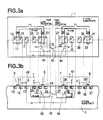
- Figure 3a is a plan view showing a semiconductor circuit according to the first embodiment of the present invention
- Fig. 3b is a sectional view thereof.
- the semiconductor circuit comprises a P-type substrate 1 on which a low-potential system (Vdd) and a high-potential system (Vpp) are formed adjacent to each other.
- the low-potential system (Vdd) comprises a first N-channel MOS transistor 3 and a first P-channel MOS transistor 5 that are complementarily connected to each other.
- the high-potential system (Vpp) comprises a second P-channel MOS transistor 7 and a second N-channel MOS transistor 9 that are complementarily connected to each other.
- the first P-channel MOS transistor 5 and second P-channel MOS transistor 7 having the same channel polarity are disposed adjacent to each other.
- the first N-channel MOS transistor 3 has a gate electrode 11, an N + drain region 13, an N + source region 15, and a P + region 17 for supplying the ground-potential to the P-type substrate 1.
- the first P-channel MOS transistor 5 has a gate electrode 19, a P + source region 21, a P + drain region 23, and an N + region 25 for supplying the Vdd-potential to an N-type well.
- the second P-channel MOS transistor 7 has a gate electrode 25, P + drain and source regions 27 and 29, and an N + region 31 for supplying the Vpp-potential to the N-type well.
- the second N-channel MOS transistor 9 has a gate electrode 33, N + source and drain regions 35 and 37, and a P + region 39 acting for supplying the ground-potential to the P-type substrate 1.
- parasitic NPN transistor 41 and parasitic PNP transistors 43 and 45 are formed.
- the parasitic PNP transistors 43 and 45 are connected in a manner similar to the conventional example of Fig. 1. In this embodiment, however, a potential of the N-well region corresponding to an emitter of the parasitic NPN transistor 41 is low (Vdd).
- the substrate potential does not increase to such an extent by the trigger current, so that the parasitic NPN transistor 41 may not be turned on to demonstrate, with the parasitic PNP transistor 45, a thyristor operation that causes an excess current to flow from a terminal 47 to a terminal 49. Namely, the latch-up phenomenon will not occur.
- the parasitic NPN transistor 41 will not demonstrate the thyristor operation because it is not turned on as explained above.
- Figure 4 shows a semiconductor circuit according to the second embodiment of the present invention.
- the semiconductor circuit comprises a P-type substrate 1 on which a low-potential system (Vdd) and a high-potential system (Vpp) are formed adjacent to each other.
- the low-potential system (Vdd) comprises a first P-channel MOS transistor 51 and a first N-channel MOS transistor 53 that are complementarily connected to each other.
- the high-potential system (Vpp) comprises a second N-channel MOS transistor 55 and a second P-channel MOS transistor 57 that are complementarily connected to each other.
- the first N-channel MOS transistor 53 and second N-channel MOS transistor 55 having the same channel polarity are disposed adjacent to each other.
- the first P-channel MOS transistor 51 has a gate electrode 57, a P + drain region 59, a P + source region 61, and an N + region 63 for supplying the Vdd-potential to an N-type well.
- the first N-channel MOS transistor 53 has a gate electrode 65, an N + source region 67, an N + drain region 69, and a P + region 71 for supplying the ground-potential to the P-type substrate 1.
- the second N-channel MOS transistor 55 has a gate electrode 73, N + drain and source regions 75 and 77, and a P + region 79 for supplying the ground-potential to the P-type substrate 1.
- the second P-channel MOS transistor 57 has a gate electrode 81, P + source and drain regions 83 and 85, and an N + region 87 for supplying the Vpp-potential to the N-type well.
- a parasitic bipolar NPN transistor 89 is formed.
- the N + diffusion region 77, P-type substrate 1 and N + diffusion region 67 from only one parasitic NPN transistor 89, so that, even if a trigger current flows to increase a potential of the P-type substrate 1, the parasitic NPN transistor 89 may not be turned on to cause a current to flow from the N + region 77 to the N + region 67.
- the embodiment does not have a parasitic PNP transistor, a thyristor conjunction is not formed to cause the latch-up phenomenon.
- N-type wells are formed in the above embodiments, P-type wells are also applicable, if potential relations are inverted. Further, a twin well structure employing P-type wells and N-type wells is also applicable.
- MOS transistors having the same channel polarity are arranged on each side of a boundary between a low-potential system and a high-potential system, so that parasitic bipolar transistors formed by the MOS transistors may not perform the thyristor operation. Accordingly, no latch-up phenomenon occurs and, unlike the conventional semiconductor circuit, no latch-up preventive diffusion region is needed.
- a distance between the transistors of the low-potential and high-potential systems can be reduced to a minimum limit allowed by a manufacturing technique.
- the arrangement can further reduce, therefore, an LSI chip area without causing the latch-up phenomenon.
Landscapes
- Metal-Oxide And Bipolar Metal-Oxide Semiconductor Integrated Circuits (AREA)
- Semiconductor Integrated Circuits (AREA)
Claims (3)
- Circuit à semi-conducteur formé dans un substrat (1) semi-conducteur d'un premier type de conductivité (P) et comprenant :une première région dudit substrat semi-conducteur dans laquelle sont formés une paire de premiers transistors MOS (3, 5 ; 51, 53) connectés de façon complémentaire, l'un (3 ; 53) desdits premiers transistors MOS étant d'un second type de conductivité (N) et l'autre (5 ; 51) desdits premiers transistors MOS étant du premier type de conductivité et étant formé dans un premier puits du second type de conductivité dans ledit substrat, lesdits premiers transistors MOS (3, 5 ; 51, 53) ayant des régions de grille, de source et de drain (11, 15, 13 ; 19, 21, 23 ; 57, 61, 59 ; 65, 67, 69) ;une première source d'alimentation pour lesdits premiers transistors MOS étant conçue pour fournir une première différence de potentiel entre un premier potentiel (Vdd) et un potentiel de masse en fournissant ledit premier potentiel à ladite source (21 ; 61) de l'un desdits premiers transistors MOS du premier type de conductivité ainsi qu'à une première région (25 ; 63) de contact de puits formée dans ledit premier puits, et en fournissant ledit potentiel de masse à ladite source (15 ; 67) de l'un desdits premiers transistors MOS du second type de conductivité ainsi qu'à une première région (17 ; 71) de contact de substrat formée dans ladite première région du substrat ;une seconde région dudit substrat semi-conducteur dans laquelle une paire de seconds transistors MOS (7, 9 ; 55, 57) connectés de façon complémentaire sont formés de façon adjacente à ladite première région, l'un (9 ; 55) desdits seconds transistors MOS étant du second type de conductivité et l'autre (7 ; 57) desdits seconds transistors MOS étant du premier type de conductivité et étant formé dans un second puits du second type de conductivité dans ledit substrat, lesdits seconds transistors MOS (7, 9 ; 55, 57) ayant des régions de grille, de source et de drain (25, 29, 27 ; 33, 35, 37 ; 73, 77, 75 ; 81, 83, 85) ;une seconde source d'alimentation pour lesdits seconds transistors MOS conçue pour fournir une seconde différence de potentiel entre un second potentiel (Vpp) et un potentiel de masse en fournissant ledit second potentiel à ladite source (29 ; 83) de l'un desdits seconds transistors MOS du premier type de conductivité ainsi qu'à une seconde région (31 ; 87) de contact de puits formée dans ledit second puits, et en fournissant ledit potentiel de masse à ladite source (35 ; 77) de l'un desdits seconds transistors MOS du second type de conductivité ainsi qu'à une seconde région (39 ; 79) de contact de substrat formée dans ladite seconde région du substrat, ledit second potentiel étant différent dudit premier potentiel ;les régions de grille, de source et de drain des premierS et secondS transistors MOS ainsi que les régions de contact de puits et de contact de substrat étant agencées suivant une rangée s'étendant dans lesdites première et seconde régions et à travers ladite frontière formée entre lesdites première et seconde régions du substrat semi-conducteur ;dans lequel les deux transistors MOS (5, 7 ; 53, 55) qui sont adjacents l'un à l'autre dans ladite rangée sur des côtés respectifs de la frontière entre lesdites première et seconde régions du substrat semi-conducteur ont la même polarité de canal ; etdans lequel ladite frontière est située dans ledit substrat semi-conducteur du premier type de conductivité, et dans lequel la séquence de types de dopage des régions de source, de drain, de puits et intermédiaire en partant de ladite frontière le long de ladite rangée dans ladite première région, est identique à la séquence de types de dopage des régions de source, de drain, de puits et intermédiaire en partant de ladite frontière le long de ladite rangée dans ladite seconde région.
- Circuit à semi-conducteur selon la revendication 1, dans lequel les transistors MOS (53, 55) desdites première et seconde régions disposées de façon adjacente les unes aux autres sur des côtés respectifs de la frontière sont chacun du type à canal N.
- Circuit à semi-conducteur selon la revendication 1, dans lequel les transistors MOS (5, 7) desdites première et seconde régions disposées de façon adjacente les unes aux autres sur des côtés respectifs de la frontière sont chacun du type à canal P.
Applications Claiming Priority (3)
| Application Number | Priority Date | Filing Date | Title |
|---|---|---|---|
| JP23985/89 | 1989-02-03 | ||
| JP2398589 | 1989-02-03 | ||
| JP1023985A JPH0770689B2 (ja) | 1989-02-03 | 1989-02-03 | 半導体回路 |
Publications (3)
| Publication Number | Publication Date |
|---|---|
| EP0381237A2 EP0381237A2 (fr) | 1990-08-08 |
| EP0381237A3 EP0381237A3 (fr) | 1991-03-27 |
| EP0381237B1 true EP0381237B1 (fr) | 1999-09-01 |
Family
ID=12125867
Family Applications (1)
| Application Number | Title | Priority Date | Filing Date |
|---|---|---|---|
| EP90102104A Expired - Lifetime EP0381237B1 (fr) | 1989-02-03 | 1990-02-02 | Circuit semi-conducteur intégré avec transistors M.O.S. à canaux P et N |
Country Status (4)
| Country | Link |
|---|---|
| EP (1) | EP0381237B1 (fr) |
| JP (1) | JPH0770689B2 (fr) |
| KR (1) | KR930001289B1 (fr) |
| DE (1) | DE69033265T2 (fr) |
Cited By (1)
| Publication number | Priority date | Publication date | Assignee | Title |
|---|---|---|---|---|
| DE19919129A1 (de) * | 1999-04-27 | 2000-11-09 | Siemens Ag | Substratkontakt für eine leitende Wanne in einer Halbleiterspeicheranordnung |
Families Citing this family (4)
| Publication number | Priority date | Publication date | Assignee | Title |
|---|---|---|---|---|
| EP0574699A2 (fr) * | 1992-05-20 | 1993-12-22 | Akzo Nobel N.V. | Membrane pour dialyse à base d'acétate de cellulose |
| US5814845A (en) * | 1995-01-10 | 1998-09-29 | Carnegie Mellon University | Four rail circuit architecture for ultra-low power and voltage CMOS circuit design |
| US6366061B1 (en) | 1999-01-13 | 2002-04-02 | Carnegie Mellon University | Multiple power supply circuit architecture |
| JP5022013B2 (ja) * | 2006-12-12 | 2012-09-12 | 株式会社豊田中央研究所 | 静電気保護用半導体装置および自動車用複合ic |
Family Cites Families (2)
| Publication number | Priority date | Publication date | Assignee | Title |
|---|---|---|---|---|
| JPS61100947A (ja) * | 1984-10-22 | 1986-05-19 | Toshiba Corp | 半導体集積回路装置 |
| JPS6273656A (ja) * | 1985-09-26 | 1987-04-04 | Toshiba Corp | 半導体装置 |
-
1989
- 1989-02-03 JP JP1023985A patent/JPH0770689B2/ja not_active Expired - Fee Related
-
1990
- 1990-02-02 KR KR1019900001270A patent/KR930001289B1/ko not_active Expired - Fee Related
- 1990-02-02 EP EP90102104A patent/EP0381237B1/fr not_active Expired - Lifetime
- 1990-02-02 DE DE69033265T patent/DE69033265T2/de not_active Expired - Fee Related
Cited By (1)
| Publication number | Priority date | Publication date | Assignee | Title |
|---|---|---|---|---|
| DE19919129A1 (de) * | 1999-04-27 | 2000-11-09 | Siemens Ag | Substratkontakt für eine leitende Wanne in einer Halbleiterspeicheranordnung |
Also Published As
| Publication number | Publication date |
|---|---|
| EP0381237A3 (fr) | 1991-03-27 |
| KR900013655A (ko) | 1990-09-06 |
| JPH0770689B2 (ja) | 1995-07-31 |
| DE69033265T2 (de) | 2000-01-05 |
| DE69033265D1 (de) | 1999-10-07 |
| KR930001289B1 (ko) | 1993-02-25 |
| EP0381237A2 (fr) | 1990-08-08 |
| JPH02205067A (ja) | 1990-08-14 |
Similar Documents
| Publication | Publication Date | Title |
|---|---|---|
| US5581104A (en) | Static discharge circuit having low breakdown voltage bipolar clamp | |
| EP0305937B1 (fr) | Protection MOS d'entrée/sortie utilisant le concept de circuit à corps commutable | |
| US6515839B1 (en) | Electronic discharge protection system for mixed voltage application specific circuit design | |
| US5796147A (en) | Semiconductor device having a plurality of circuits driven by different power sources and formed on the same substrate | |
| EP0782192B1 (fr) | Structure de décharges électrostatiques pour un dispositif semi-conducteur | |
| US4647956A (en) | Back biased CMOS device with means for eliminating latchup | |
| KR0159451B1 (ko) | 반도체장치의 보호회로 | |
| US6215135B1 (en) | Integrated circuit provided with ESD protection means | |
| WO2001045173A1 (fr) | Structure de diode esd amelioree | |
| KR100738153B1 (ko) | 기판 바이어싱을 위하여 수평 pnp 또는 pmos 또는양자를 사용하는 정전 방전 보호용 시스템 및 방법 | |
| US5763918A (en) | ESD structure that employs a schottky-barrier to reduce the likelihood of latch-up | |
| EP1048076B1 (fr) | Redresseur a thyristors a tension de maintien et de declenchement faible pour la protection contre les decharges electrostatiques | |
| US5357126A (en) | MOS transistor with an integrated protection zener diode | |
| JP3559075B2 (ja) | Cmos技術の集積電子回路用の極性反転保護装置 | |
| US6624479B2 (en) | Semiconductor device having a protective circuit | |
| EP0381237B1 (fr) | Circuit semi-conducteur intégré avec transistors M.O.S. à canaux P et N | |
| US5760447A (en) | Semiconductor device having pull-up or pull-down resistance | |
| US6580592B2 (en) | Semiconductor device | |
| US4812891A (en) | Bipolar lateral pass-transistor for CMOS circuits | |
| US5892263A (en) | CMOS device connected to at least three power supplies for preventing latch-up | |
| US6084272A (en) | Electrostatic discharge protective circuit for semiconductor device | |
| JPS6197858A (ja) | 半導体装置 | |
| US6583475B2 (en) | Semiconductor device | |
| KR100270949B1 (ko) | 극성에 상관없이 내부 회로를 보호하기 위하여 전원 공급 단자들 사이에 적용한 정전기 방지 회로 | |
| JPH044755B2 (fr) |
Legal Events
| Date | Code | Title | Description |
|---|---|---|---|
| PUAI | Public reference made under article 153(3) epc to a published international application that has entered the european phase |
Free format text: ORIGINAL CODE: 0009012 |
|
| 17P | Request for examination filed |
Effective date: 19900202 |
|
| AK | Designated contracting states |
Kind code of ref document: A2 Designated state(s): DE FR GB |
|
| PUAL | Search report despatched |
Free format text: ORIGINAL CODE: 0009013 |
|
| AK | Designated contracting states |
Kind code of ref document: A3 Designated state(s): DE FR GB |
|
| 17Q | First examination report despatched |
Effective date: 19930525 |
|
| GRAG | Despatch of communication of intention to grant |
Free format text: ORIGINAL CODE: EPIDOS AGRA |
|
| GRAG | Despatch of communication of intention to grant |
Free format text: ORIGINAL CODE: EPIDOS AGRA |
|
| GRAH | Despatch of communication of intention to grant a patent |
Free format text: ORIGINAL CODE: EPIDOS IGRA |
|
| GRAH | Despatch of communication of intention to grant a patent |
Free format text: ORIGINAL CODE: EPIDOS IGRA |
|
| GRAA | (expected) grant |
Free format text: ORIGINAL CODE: 0009210 |
|
| AK | Designated contracting states |
Kind code of ref document: B1 Designated state(s): DE FR GB |
|
| REF | Corresponds to: |
Ref document number: 69033265 Country of ref document: DE Date of ref document: 19991007 |
|
| ET | Fr: translation filed | ||
| PLBE | No opposition filed within time limit |
Free format text: ORIGINAL CODE: 0009261 |
|
| STAA | Information on the status of an ep patent application or granted ep patent |
Free format text: STATUS: NO OPPOSITION FILED WITHIN TIME LIMIT |
|
| 26N | No opposition filed | ||
| REG | Reference to a national code |
Ref country code: GB Ref legal event code: IF02 |
|
| PGFP | Annual fee paid to national office [announced via postgrant information from national office to epo] |
Ref country code: DE Payment date: 20060126 Year of fee payment: 17 |
|
| PGFP | Annual fee paid to national office [announced via postgrant information from national office to epo] |
Ref country code: GB Payment date: 20060201 Year of fee payment: 17 |
|
| PGFP | Annual fee paid to national office [announced via postgrant information from national office to epo] |
Ref country code: FR Payment date: 20060220 Year of fee payment: 17 |
|
| GBPC | Gb: european patent ceased through non-payment of renewal fee |
Effective date: 20070202 |
|
| REG | Reference to a national code |
Ref country code: FR Ref legal event code: ST Effective date: 20071030 |
|
| PG25 | Lapsed in a contracting state [announced via postgrant information from national office to epo] |
Ref country code: DE Free format text: LAPSE BECAUSE OF NON-PAYMENT OF DUE FEES Effective date: 20070901 |
|
| PG25 | Lapsed in a contracting state [announced via postgrant information from national office to epo] |
Ref country code: GB Free format text: LAPSE BECAUSE OF NON-PAYMENT OF DUE FEES Effective date: 20070202 Ref country code: FR Free format text: LAPSE BECAUSE OF NON-PAYMENT OF DUE FEES Effective date: 20070228 |