EP0380926A2 - Asynchronous microprocessor random access memory arbitration controller - Google Patents
Asynchronous microprocessor random access memory arbitration controller Download PDFInfo
- Publication number
- EP0380926A2 EP0380926A2 EP90100331A EP90100331A EP0380926A2 EP 0380926 A2 EP0380926 A2 EP 0380926A2 EP 90100331 A EP90100331 A EP 90100331A EP 90100331 A EP90100331 A EP 90100331A EP 0380926 A2 EP0380926 A2 EP 0380926A2
- Authority
- EP
- European Patent Office
- Prior art keywords
- access
- microprocessor
- common memory
- memory
- controller according
- Prior art date
- Legal status (The legal status is an assumption and is not a legal conclusion. Google has not performed a legal analysis and makes no representation as to the accuracy of the status listed.)
- Withdrawn
Links
Images


Classifications
-
- G—PHYSICS
- G06—COMPUTING; CALCULATING OR COUNTING
- G06F—ELECTRIC DIGITAL DATA PROCESSING
- G06F15/00—Digital computers in general; Data processing equipment in general
- G06F15/16—Combinations of two or more digital computers each having at least an arithmetic unit, a program unit and a register, e.g. for a simultaneous processing of several programs
- G06F15/163—Interprocessor communication
- G06F15/167—Interprocessor communication using a common memory, e.g. mailbox
-
- G—PHYSICS
- G06—COMPUTING; CALCULATING OR COUNTING
- G06F—ELECTRIC DIGITAL DATA PROCESSING
- G06F13/00—Interconnection of, or transfer of information or other signals between, memories, input/output devices or central processing units
- G06F13/14—Handling requests for interconnection or transfer
- G06F13/16—Handling requests for interconnection or transfer for access to memory bus
- G06F13/1605—Handling requests for interconnection or transfer for access to memory bus based on arbitration
- G06F13/1652—Handling requests for interconnection or transfer for access to memory bus based on arbitration in a multiprocessor architecture
- G06F13/1663—Access to shared memory
Definitions
- the present invention generally, relates to data processing computer systems and, more particularly, to a new and improved system of arbitration for access to a random access memory unit by a plurality of asynchronous microprocessor devices.
- microprocessors that are arranged to use the "wait" signal (in contrast with a “not ready” signal) stop functioning at cycle boundaries. Then, such microprocessors release their control lines to other devices.
- U.S. Patent No. 4,096,572 issued in June 1978 teaches the use of a handshake system with a "wait" signal, if there is a memory access conflict.
- a request for access to the common memory is responded to by an "acknowledge” or a "wait” signal, and processors provide memory access timing.
- the present invention does not use a request/acknowledgement handshake method, as will be understood better as the description proceeds.
- the present invention not only provides such an arbitration control device but reduces the usual cost of these devices while, in addition, providing other desirable and useful features, as will become more readily apparent.
- the present invention provides a system of arbitration for access to a common memory by two microprocessor without excluding either microprocessor for more than a predetermined, limited period of time.
- An arbitration system in accordance with the invention includes two microprocessors connected to a common memory unit through an arbitration controller with a connection to convey a "not ready” signal to a microprocessor requesting access to the memory when the other microprocessor has access.
- the "not ready” signal stops the requesting microprocessor during its cycle.
- the arbitration system re-creates the timing up to the point that the requesting microprocessor was stopped, removes the "not ready” condition when the cycle of the common memory is ready to permit access and allows the requesting microprocessor to complete its cycle of operation. Thereafter, the requesting microprocessor does not exist on all microprocessors. It stops normal operations of the microprocessor at the point in its cycle that it receives a "not ready” signal from the common memory.
- a "not ready” mode is the state of a microprocessor when the "not ready” condition is present and is controlled by the arbiter. It is the arbiter controls that must re-create the timing sequence in the microprocessor up to the point at which the normal operation of the microprocessor was interrupted, remove the "not ready” condition, and allow the microprocessor to complete its interrupted cycle.
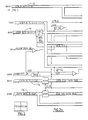
- a MAIN microprocessor is identified by the reference numeral 10
- a TASK microprocessor is identified by the reference numeral 11.
- the TASK microprocessor 11 interfaces the printer control unit to several different kinds of data processing systems. Each type of data processing system manner. This is a form of "contention", as will be described more fully presently.
- active and inactive is meant only that the signal is a “one” or a “zero”.
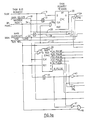
- a second flip flop device 23 is connected to an OR gate 24 through which, when the flip flop 20 is "on", a terminal D on the flip flop device 23 is active.
- the flip flop 23 must be turned “on”, and to accomplish this, two signals are needed, one from the “not on” terminal 25 of the flip flop 23 and the other from the MAIN clockout 22 in order to apply a signal to the "clk” terminal of the flip flop 23 through an AND gate 26. This condition is in existence now, and so, there is an output from the AND gate 26 and the flip flop 23 is turned “on”.
- the MAIN clockout clock pulse is the signal that clocks the entire system, in accordance with the invention.
- the cycle just described above is a two-step sequence: first, the "TASK request pending" flip flop 20 is turned “on”, because there is a “contention” between the two microprocessors for access to the common memory 14, and second, the TASK RAM cycle flip flop 23 is turned “on” as described. Now, with the flip flop 23 turned “on”, the TASK microprocessor will be synchronized with the MAIN clockout signal on connection 22.
- the only time that the TASK request pending flip flop 20 is used, according to the invention, is when there is contention.
- the TASK microprocessor requests access to the common memory 14 and the MAIN microprocessor is not using the common memory, the only thing to be done is to synchronize the TASK microprocessor with the MAIN clockout signal on connection 22 which is done with a signal on the input connection 24 a to the OR gate 24.
- an AND gate To develop a signal on the input connection 24 a to the OR gate 24, an AND gate must have two signal inputs.
- One input signal on connection 28 is from the TASK bus request to indicate that the TASK microprocessor needs access to the common memory 14, and the second input signal on connection 29 indicates that the MAIN microprocessor is not using the common memory.
- the flip flop 20 is needed, and if there is no contention, only the flip flop 23 is needed. In both of these situations, however, the flip flop 23 is used because it is needed to start the synchronism procedure for synchronizing the TASK microprocess with the MAIN clockout signal on connection 22.
- connection 30 has an "active" signal, and this is applied to one terminal of an AND gate 31.
- the system of the invention uses the MAIN clockout signal on line 22. It is a free-running clock at a frequency that is predetermined, in the present invention as used in a printer apparatus, it runs at 7.5 mega-Hertz, meaning it cycles once every 133 nano-seconds. Of course, its frequency can be set to correspond with a particular use. But it is the base clock in this use, and it is running whenever the printer power is turned on.
- the flip flop devices 20 and 23 are a type known as "D" type flip flops, which require two conditions for one to be turned “on”, as will be understood readily by one skilled in the art. First the signal on the D terminal must be active, and second, there must be an edge on the signal at the "clk” terminal. An “edge” is a transition for the signal on the "clk” terminal. On the other hand, if the signal at the terminal D is not active, a transition at the "clk” terminal will cause the flip flop to turn “off”.
- the "clk” on the shift register 32 is slightly different.
- the use of the shift register 32 is to provide a source of signals in a predetermined sequence or in some other desired manner.
- the pulses out from the shift register 32 are labeled "A” through “G”, and these pulses are generated only when the input terminal "D" on the shift register 32 is active, a condition which is controlled by an AND gate 31.
- the AND gate 31 develops a signal to turn the terminal "D" of the shift register 32 "on” when its input is satisfied, which is when the flip flop 23 is turned “on” and there is an active signal on the connection 30 and when a LATCH device 33 is turned “off”.
- the AND gate is developing an active signal, or a "1"
- the MAIN clockout signal goes from a negative to a positive, that causes the first pulse to be developed by the shift register 32, which is an "A" pulse.
- each flip flop 20 and 23 can be reset by a general reset condition in the printer control unit, which is a "machine reset" signal on the connection 34 through an OR gate 35 a .
- the TASK request pending flip flop 20 is reset logically when the TASK RAM cycle flip flop 23 is turned “on”.
- the TASK RAM cycle flip flop 23 is reset through an OR gate 35 b by a machine reset signal, or a TASK bus request long signal, or a signal from an AND gate 35 c .
- the signal from the AND gate 35 c is the normal reset signal for the flip flop 23.
- the MAIN microprocessor is prevented from obtaining access to the common memory 14 while the TASK microprocessor completes its cycle of the common memory.
- the signal on the connection 30 is not active, because the flip flop 23 turns "off", and therefore, at this time, the MAIN microprocessor may obtain access for its cycle of the common memory.
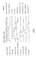
- line No. 1 with the identity legend "MAIN clockout” shows the 133 nano-second (7.5 MHz) clock signal to which an asynchronous TASK microprocessor, according to the invention, is synchronized.
- the other signals are identified by appropriate legends also so that the interaction of the respective components is readily understandable without much additional effort.
- item No. 2 shows that the TASK Bus Request has been asserted, and now, moving down to item No. 6 shows when the TASK RAM cycle flip flop turns "on".
- item No. 6 shows when the TASK RAM cycle flip flop turns "on".
- "1.2. 3 is indicated, which in words, reads, "one.two.not 3”. This can be translated to say, “item No. 1 is needed, item No. 2 is needed and not item No. 3" in order to accomplish this item No. 6.
- each LATCH device, 33, 40 and 41 simply involves a set terminal "S” and a reset terminal “R” as inputs in order to turn each one "on”, meaning the "Q" terminal is active (or “1"). This means simply that a "set” turns a LATCH "on”, and a “reset” turns a LATCH "off”.
- an "A" pulse from the shift register 32 will cause the LATCH 40 to turn “on”, providing an active condition (or a "1" signal) at its "Q" output terminal. This condition remains until a reset occurs, which is in one of two ways.
- An OR gate 42 connects one or the other of two signals to the reset terminal. The uppermost connection to the OR gate 42 connects with the "machine reset" signal, provided by a general condition in the printer control unit. The lowermost connection to the OR gate 42 is a logical connection for the signal provided by the invention as follows.
- An AND gate 43 provides a logical signal when there is a "D" pulse from the shift register 32 plus NOT a MAIN clockout signal (note the inverter "N” identified also by the numeral 44). When this occurs, the TASK Bus Acknowledge connection goes from a “one” to a “zero”, or is turned “off”. Looking at FIG. 5 reveals exactly how this appears (in item No. 8) and when, (or its relative timing).
- the operation of the other LATCH devices can be understood readily.
- the LATCH device 33 it is turned “on” by a set signal to its "S" terminal from the A pulse output from the shift register 32 directly, and it is turned “off” or reset by a G pulse.
- the LATCH device is "on” for a longer period of time, by item No. 9 being “on” from the beginning of the A pulse to the beginning of the G pulse.
- the G pulse is connected through an OR gate 45, the other terminal being the same "machine reset" signal described above.
- the final LATCH device 41 is used in this logic circuit for detail memory controls. Functionally, it is not an important device in accomplishing the purposes of the invention and is included for completeness of the disclosure.
- This LATCH is set by the B pulse from the shift register 32 to provide a signal output on the TASK RAM gate bus, as shown.
- the LATCH device 41 is reset by either the same "machine reset" signal described previously through an OR gate 46 or by an output from an AND gate 47.
- One of the two input connections to the AND gate 47 is by a connection from the same inverter 44 described previously in connection with LATCH 40 and the other input connection is from the C pulse output of the shift register 32.
- the shift register 32 provides any number of pulses of any desired duration for any needed control purpose.
- One important purpose accomplished by the shift register 32 is control of access by the MAIN microprocessor to the common memory, particularly when the TASK microprocessor needs access.
- each of the two microprocessors have access to the common memory for a shared, predetermined, limited period of time. In this embodiment, that limited period of time is for one cycle of the common memory.
- Still another important use of the shift register, according to the invention, is to synchronize the two asynchronous microprocessors.
- the "clk" terminal of the shift register 32 is connected directly with the MAIN clockout signal of the MAIN microprocessor so that the various pulses output from the shift register 32 are synchronized with the MAIN microprocessor.
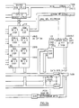
- FIG. 2 of the drawings shows the various input/output connections for a particularly arranged random access memory unit, identified with the legend "COMMON MEMORY”.
- This unit is common to two microprocessors, one being identified with the legend "Main” and the other with the legend "Task”.
- the Main microprocessor that is used in this presently preferred embodiment is an Intel 80186 that is available commercially from the Intel Corporation.
- the particular random access memory unit in FIG. 2 has a total of 32K bytes of memory that is used by the Main microprocessor, 4K of which is shared with the Task microprocessor.
- This random access memory unit also contains l6k bytes of Read Only Memory (ROM) which is available only to the Main microprocessor.
- ROM Read Only Memory
- the parallel interface to the Main microprocessor consists of address, control and data (2 bi-directional bytes) signals to access the Random Access Memory (RAM) and the ROM (or the EPROM). Access to the RAM by the Main microprocessor will be more frequent than by the Task microprocessor because all of the Main microprocessor's working memory is contained within the circuit of FIG. 2. It should be noted also that parity checkers are included in this circuit to verify data integrity for RAM accesses for both data bytes.
- FIG. 2 there is shown also the parallel interface to the Task microprocessor consists of address, control and data (1 bi-directional byte) signals.
- the purpose of this parallel interface is to allow Task access to the 4KB RAM that is shared with the Main microprocessor. During operations, this part of the RAM is used to pass control and data information back and forth between the two microprocessors.
- FIG. 3 contains all of the arbitration controls to designate that the Main microprocessor can not perform two back-to-back accesses to the common memory while the Task microprocessor is requesting access. If the Task microprocessor initiates a request for access while the Main microprocessor is accessing the RAM, the Task microprocessor must wait until the Main microprocessor completes a cycle of its access to the RAM. At the completion of the MAIN microprocessor cycle, the TASK bus request signal will set the TASK RAM flip flop, as previously described, and cause the shift register 32 to activate the LATCH 40 to generate a TASK bus acknowledge signal. This signal is the beginning of the TASK cycle.
- neither microprocessor is locked out for more than a predetermined period of time which, in the preferred embodiment, is one cycle of RAM time.
- the arbitration controller of the invention gives priority to the Main microprocessor, but upon completion of one cycle of access time, access by the Main microprocessor is interrupted while the Task microprocessor has access for one cycle.
- FIG. 3 of the drawings show the arbitration controls to accomplish the above-described routines.
- the various legends included directly in all of the FIGs. of the drawings permit one skilled in this art to understand these circuit arrangements, and therefore, this written description is only supplemental to the full disclosure of the drawings.
- the TASK Request Pending FF will only be set to indicate that the TASK microprocessor has requested a cycle of access time with the common memory, and this indication is given only while the Main microprocessor is accessing the RAM, i.e., during its turn with the Common Memory. Thereafter, as described above, the Task microprocessor will be granted access for the next memory cycle, which will be indicated by the set of the Task RAM Cycle FF.
- All of the logic in FIG. 3 is activated only to control the Common Memory for a Task microprocessor turn at a RAM cycle.
- All of the logic in FIG. 3 is degated.
- FIG 4 and FIG. 5 show details of the timing relative to priority arbitration, as well as memory cycles for both of the microprocessors. It is believed that all of the legends included directly on these drawings will be more than sufficient to understand their function and operation. For example, the timing for operation of the block, in FIG. 3, with the legend "Shift Reg. (164)" is given clearly in FIG. 4 of the drawings.
Abstract
Description
- The present invention, generally, relates to data processing computer systems and, more particularly, to a new and improved system of arbitration for access to a random access memory unit by a plurality of asynchronous microprocessor devices.
- It is common practice in networks having multiple microprocessors that two of the microprocessors will share large amounts of memory. It is known also that, as between two such microprocessors, a system of arbitration must be provided to control their access to the common memory. The problem is compounded when the microprocessors are asynchronous.
- There are many off-the-shelf vendor components available today that have Dual Port Memory Controls which include various amounts of memory with each module, but a difficulty is experienced in attempting to use them with microprocessors that are asynchronous. Another difficulty with such components available today is that the memory associated with these components are too small or that the memory controls do not match the control need as between two microprocessors because of a mismatch with the synchronism of the microprocessors.
- In the past, it has been customary in a device utilizing a plurality of microprocessors for one microprocessor to be connected to a memory unit to the exclusion of the others. Other microprocessors may obtain access only while the memory unit is "idle".
- It was recognized early in the art that if the common memory unit could be utilized more efficiently, the efficiency of the whole computer network would be improved. Thereafter, the search was on to develop a wide variety of systems, techniques and/or devices to permit such improvement.
- From about the mid 1970's to about the mid 1980's, the search for an improvement in the overall efficiency of utilization of a common memory as between at least two memory utilization devices was most intense. However, many arrangements developed during this period used a system involving a "wait" signal to identify the microprocessor that was to be denied access to the common memory.
- The microprocessors that are arranged to use the "wait" signal (in contrast with a "not ready" signal) stop functioning at cycle boundaries. Then, such microprocessors release their control lines to other devices.
- An early U.S. Patent No. 4,065,809 was issued in 1977 and involves two synchronous CPU's with a simple flip-flop to render one CPU inactive when the other CPU is active. While effective in a simple arithmetic environment, this arrangement is inoperative in a complex environment in which the present invention is adapted to function.
- U.S. Patent No. 4,096,572 issued in June 1978 teaches the use of a handshake system with a "wait" signal, if there is a memory access conflict. A request for access to the common memory is responded to by an "acknowledge" or a "wait" signal, and processors provide memory access timing. The present invention does not use a request/acknowledgement handshake method, as will be understood better as the description proceeds.
- U.S. Patent No. 4,121,285 issued in October 1978 teaches that, when several devices must access a common unit, equal priority is provided. This arrangement only determines priority and does not provide for any access timing, as with the present invention.
- U.S. Patent No. 4,128,881 issued then in December 1978 provides a different, pre-fixed address for each processor that must have access to a common memory. This arrangement does not involve a need to determine priority between the processors and, therefore, is completely at variance with the present invention.
- A more recent U.S. Patent No. 4,542,454 issued in September 1985 is entitled "Apparatus for Controlling Access To A Memory". However, its system is for access to a memory by a single processor for different purposes. It teaches using a
dynamic memory controller 26 to obtain access under four different modes or functions, such as (1) refresh without error detection, (2) refresh with error detection, (3) clear and (4) read/write. - Therefore, the need still exists today for a control to arbitrate effectively between two asynchronous microprocessors in a network having a common memory. The present invention not only provides such an arbitration control device but reduces the usual cost of these devices while, in addition, providing other desirable and useful features, as will become more readily apparent.
- Accordingly, it is a principal object of the present invention to provide an arbitration controller for use with asynchronous microprocessors.
- It is also an object of the present invention to provide a system of arbitration for access to a memory that is common to two microprocessors.
- Briefly, the present invention provides a system of arbitration for access to a common memory by two microprocessor without excluding either microprocessor for more than a predetermined, limited period of time. An arbitration system in accordance with the invention includes two microprocessors connected to a common memory unit through an arbitration controller with a connection to convey a "not ready" signal to a microprocessor requesting access to the memory when the other microprocessor has access. The "not ready" signal stops the requesting microprocessor during its cycle. The arbitration system re-creates the timing up to the point that the requesting microprocessor was stopped, removes the "not ready" condition when the cycle of the common memory is ready to permit access and allows the requesting microprocessor to complete its cycle of operation. Thereafter, the requesting microprocessor does not exist on all microprocessors. It stops normal operations of the microprocessor at the point in its cycle that it receives a "not ready" signal from the common memory.
- A "not ready" mode is the state of a microprocessor when the "not ready" condition is present and is controlled by the arbiter. It is the arbiter controls that must re-create the timing sequence in the microprocessor up to the point at which the normal operation of the microprocessor was interrupted, remove the "not ready" condition, and allow the microprocessor to complete its interrupted cycle.
- Before presenting a detailed description of the respective figures 1-5b in the drawings, an identification of the abbreviations used in these figures is given in the following Glossary of terms:
ALE Address Latch Enable
ARDY Asynchronous ready
BHE Bus high enable
CTRLS Controls
DEN Data bus enable
DIAG Diagnostic
DRV Driver
DT/R Data transmit/receive
FF Flip flop
EPROM Electrically programmable read only memory
I/O Input/output
IRPT Interrupt
LCS Lower memory chip select
MCS Mid memory chip select
N Inverter circuit
NMI Non-maskable interrupt
OE Output enable
PCS Peripheral chip select
PTY Parity
PTY CHK Parity checker
RAM Random access memory
RD Read
ROM Read only memory
RST Reset
TBA Task bus acknowledge
TBR Task bus request
TXC Task transfer complete
WR Write
UCS Upper memory chip select
UP Microprocessor
XCVR Transceiver - Referring first to FIG. 1 of the drawings, a MAIN microprocessor is identified by the
reference numeral 10, and a TASK microprocessor is identified by thereference numeral 11. TheTASK microprocessor 11 interfaces the printer control unit to several different kinds of data processing systems. Each type of data processing system manner. This is a form of "contention", as will be described more fully presently. - Referring to FIG. 2 and to FIG. 3, at the completion of each cycle of the
common memory 14, the signal on thebus 18, also identified as "MAIN Select", goes inactive. This signal is active during each cycle of the common memory, and at the end of each cycle, it goes inactive. If the TASK microprocessor needs access to thecommon memory 14, an active signal is applied on aconnection 19 and to a terminal D of aflip flop device 20. By "active" and "inactive", is meant only that the signal is a "one" or a "zero". - At the end of a cycle of the
MAIN microprocessor 10, the signal on thebus 18 goes inactive, which applies a clock signal at a "clk" terminal on theflip flop 20, but since the two microprocessors are asynchronous, synchronism must be obtained with the MAIN clockout signal. To accomplish this, according to the invention, a secondflip flop device 23 is connected to anOR gate 24 through which, when theflip flop 20 is "on", a terminal D on theflip flop device 23 is active. - At this point in the cycle being described, the
flip flop 23 must be turned "on", and to accomplish this, two signals are needed, one from the "not on"terminal 25 of theflip flop 23 and the other from the MAIN clockout 22 in order to apply a signal to the "clk" terminal of theflip flop 23 through an ANDgate 26. This condition is in existence now, and so, there is an output from the ANDgate 26 and theflip flop 23 is turned "on". - The MAIN clockout clock pulse is the signal that clocks the entire system, in accordance with the invention.
- The cycle just described above is a two-step sequence: first, the "TASK request pending"
flip flop 20 is turned "on", because there is a "contention" between the two microprocessors for access to thecommon memory 14, and second, the TASK RAMcycle flip flop 23 is turned "on" as described. Now, with theflip flop 23 turned "on", the TASK microprocessor will be synchronized with the MAIN clockout signal onconnection 22. - It should be noted that the only time that the TASK request pending
flip flop 20 is used, according to the invention, is when there is contention. When the TASK microprocessor requests access to thecommon memory 14 and the MAIN microprocessor is not using the common memory, the only thing to be done is to synchronize the TASK microprocessor with the MAIN clockout signal onconnection 22 which is done with a signal on the input connection 24a to theOR gate 24. - To develop a signal on the input connection 24a to the
OR gate 24, an AND gate must have two signal inputs. One input signal onconnection 28 is from the TASK bus request to indicate that the TASK microprocessor needs access to thecommon memory 14, and the second input signal onconnection 29 indicates that the MAIN microprocessor is not using the common memory. - There are only two situations, one when there is contention and the other when there is no contention. If there is contention, the
flip flop 20 is needed, and if there is no contention, only theflip flop 23 is needed. In both of these situations, however, theflip flop 23 is used because it is needed to start the synchronism procedure for synchronizing the TASK microprocess with the MAIN clockout signal onconnection 22. - Therefore, the synchronization of any TASK microprocessor with the MAIN clock signal is accomplished by, first turning "on" the
flip flop 23, as described above. Now, theconnection 30 has an "active" signal, and this is applied to one terminal of an ANDgate 31. - Every system must have a clock to control its activities in an orderly and predictable manner. The system of the invention uses the MAIN clockout signal on
line 22. It is a free-running clock at a frequency that is predetermined, in the present invention as used in a printer apparatus, it runs at 7.5 mega-Hertz, meaning it cycles once every 133 nano-seconds. Of course, its frequency can be set to correspond with a particular use. But it is the base clock in this use, and it is running whenever the printer power is turned on. - The
flip flop devices - The "clk" on the
shift register 32 is slightly different. The use of theshift register 32 is to provide a source of signals in a predetermined sequence or in some other desired manner. For the present use, the pulses out from theshift register 32 are labeled "A" through "G", and these pulses are generated only when the input terminal "D" on theshift register 32 is active, a condition which is controlled by an ANDgate 31. - The AND
gate 31 develops a signal to turn the terminal "D" of theshift register 32 "on" when its input is satisfied, which is when theflip flop 23 is turned "on" and there is an active signal on theconnection 30 and when a LATCH device 33 is turned "off". At this time in each cycle, i.e., when the AND gate is developing an active signal, or a "1", when the MAIN clockout signal goes from a negative to a positive, that causes the first pulse to be developed by theshift register 32, which is an "A" pulse. - Now, when the next transition occurs on the MAIN clockout signal, the "A" pulse ends and a "B" pulse is developed, and so forth. This pulse sequence is illustrated clearly on
line 3 of FIG. 4. - To describe the RESET function of the "Rst" terminal on each
flip flop flip flop 20 is reset logically when the TASK RAMcycle flip flop 23 is turned "on". The TASK RAMcycle flip flop 23 is reset through an ORgate 35b by a machine reset signal, or a TASK bus request long signal, or a signal from an ANDgate 35c. The signal from the ANDgate 35c is the normal reset signal for theflip flop 23. - If a signal on
connection 36, with a legend also of "MAIN ARDY", is not active, the MAIN microprocessor is prevented from obtaining access to the common memory and is made "not ready". Such a signal is developed by the ANDgate 38 through aninverter 37 in response to the signal on the MAINselect connection 18 plus either (due to OR gate 39) the LATCH 33 being turned "on" or the TASK RAMcycle flip flop 23 being turned "on". - By the means of the lock signal on the
connection 36 the MAIN microprocessor is prevented from obtaining access to thecommon memory 14 while the TASK microprocessor completes its cycle of the common memory. At the end of this cycle, the signal on theconnection 30 is not active, because theflip flop 23 turns "off", and therefore, at this time, the MAIN microprocessor may obtain access for its cycle of the common memory. - Note that, in FIG. 5, line No. 1 with the identity legend "MAIN clockout" shows the 133 nano-second (7.5 MHz) clock signal to which an asynchronous TASK microprocessor, according to the invention, is synchronized. The other signals are identified by appropriate legends also so that the interaction of the respective components is readily understandable without much additional effort.
- For example, item No. 2 shows that the TASK Bus Request has been asserted, and now, moving down to item No. 6 shows when the TASK RAM cycle flip flop turns "on". At the beginning of this pulse, note that "1.2.
3 " is indicated, which in words, reads, "one.two.not 3". This can be translated to say, "item No. 1 is needed, item No. 2 is needed and not item No. 3" in order to accomplish this item No. 6. - In FIG. 3 of the drawings, note that two
LATCH devices - Consider the
LATCH 40 first, an "A" pulse from theshift register 32 will cause theLATCH 40 to turn "on", providing an active condition (or a "1" signal) at its "Q" output terminal. This condition remains until a reset occurs, which is in one of two ways. An ORgate 42 connects one or the other of two signals to the reset terminal. The uppermost connection to theOR gate 42 connects with the "machine reset" signal, provided by a general condition in the printer control unit. The lowermost connection to theOR gate 42 is a logical connection for the signal provided by the invention as follows. - An AND
gate 43 provides a logical signal when there is a "D" pulse from theshift register 32 plus NOT a MAIN clockout signal (note the inverter "N" identified also by the numeral 44). When this occurs, the TASK Bus Acknowledge connection goes from a "one" to a "zero", or is turned "off". Looking at FIG. 5 reveals exactly how this appears (in item No. 8) and when, (or its relative timing). - With this description, the operation of the other LATCH devices can be understood readily. For example, take the LATCH device 33, it is turned "on" by a set signal to its "S" terminal from the A pulse output from the
shift register 32 directly, and it is turned "off" or reset by a G pulse. From the timing chart in FIG. 5, it can be seen that the LATCH device is "on" for a longer period of time, by item No. 9 being "on" from the beginning of the A pulse to the beginning of the G pulse. The G pulse is connected through anOR gate 45, the other terminal being the same "machine reset" signal described above. - The
final LATCH device 41 is used in this logic circuit for detail memory controls. Functionally, it is not an important device in accomplishing the purposes of the invention and is included for completeness of the disclosure. This LATCH is set by the B pulse from theshift register 32 to provide a signal output on the TASK RAM gate bus, as shown. TheLATCH device 41 is reset by either the same "machine reset" signal described previously through anOR gate 46 or by an output from an ANDgate 47. One of the two input connections to the ANDgate 47 is by a connection from thesame inverter 44 described previously in connection withLATCH 40 and the other input connection is from the C pulse output of theshift register 32. - While only the
LATCH devices shift register 32 provides any number of pulses of any desired duration for any needed control purpose. One important purpose accomplished by theshift register 32 is control of access by the MAIN microprocessor to the common memory, particularly when the TASK microprocessor needs access. - By this means of control, neither microprocessor is locked out of such access for a lengthy period of time. According to the invention, each of the two microprocessors have access to the common memory for a shared, predetermined, limited period of time. In this embodiment, that limited period of time is for one cycle of the common memory.
- Still another important use of the shift register, according to the invention, is to synchronize the two asynchronous microprocessors. The "clk" terminal of the
shift register 32 is connected directly with the MAIN clockout signal of the MAIN microprocessor so that the various pulses output from theshift register 32 are synchronized with the MAIN microprocessor. - As described previously hereinabove, FIG. 2 of the drawings shows the various input/output connections for a particularly arranged random access memory unit, identified with the legend "COMMON MEMORY". This unit is common to two microprocessors, one being identified with the legend "Main" and the other with the legend "Task".
- While the legend "Task" is termed a microprocessor in the following description, it is actually more because the legend "Task" is an interface or an adapter since it interconnects an entire host system to the printer control unit, FIG. 1. Therefore, it will be understood that the legend "Task" is called a microprocessor in this description for convenience. To be absolutely accurate, the legend "Task" identifies an Adapter Microprocessor Interface.
- The Main microprocessor that is used in this presently preferred embodiment is an Intel 80186 that is available commercially from the Intel Corporation.
- The particular random access memory unit in FIG. 2 has a total of 32K bytes of memory that is used by the Main microprocessor, 4K of which is shared with the Task microprocessor. This random access memory unit also contains l6k bytes of Read Only Memory (ROM) which is available only to the Main microprocessor.
- There is shown also in FIG. 2 that the parallel interface to the Main microprocessor consists of address, control and data (2 bi-directional bytes) signals to access the Random Access Memory (RAM) and the ROM (or the EPROM). Access to the RAM by the Main microprocessor will be more frequent than by the Task microprocessor because all of the Main microprocessor's working memory is contained within the circuit of FIG. 2. It should be noted also that parity checkers are included in this circuit to verify data integrity for RAM accesses for both data bytes.
- In FIG. 2, there is shown also the parallel interface to the Task microprocessor consists of address, control and data (1 bi-directional byte) signals. The purpose of this parallel interface is to allow Task access to the 4KB RAM that is shared with the Main microprocessor. During operations, this part of the RAM is used to pass control and data information back and forth between the two microprocessors.
- It should be noted that FIG. 3 contains all of the arbitration controls to designate that the Main microprocessor can not perform two back-to-back accesses to the common memory while the Task microprocessor is requesting access. If the Task microprocessor initiates a request for access while the Main microprocessor is accessing the RAM, the Task microprocessor must wait until the Main microprocessor completes a cycle of its access to the RAM. At the completion of the MAIN microprocessor cycle, the TASK bus request signal will set the TASK RAM flip flop, as previously described, and cause the
shift register 32 to activate theLATCH 40 to generate a TASK bus acknowledge signal. This signal is the beginning of the TASK cycle. - At this point, assume that the Main microprocessor has not completed its need for access to the RAM. It is nevertheless put on hold by a "not ready" signal for one cycle of the RAM, while the Task microprocessor completes its one cycle of RAM access time. Thus, the two microprocessors alternate access to the RAM until each has completed its need for access.
- By this procedure, neither microprocessor is locked out for more than a predetermined period of time which, in the preferred embodiment, is one cycle of RAM time. However, if both microprocessors request access to the common memory at the same time, the arbitration controller of the invention gives priority to the Main microprocessor, but upon completion of one cycle of access time, access by the Main microprocessor is interrupted while the Task microprocessor has access for one cycle.
- FIG. 3 of the drawings show the arbitration controls to accomplish the above-described routines. The various legends included directly in all of the FIGs. of the drawings permit one skilled in this art to understand these circuit arrangements, and therefore, this written description is only supplemental to the full disclosure of the drawings.
- For example, it is understood that the block in FIG. 3 with the legend "N" that is in the connection labeled "MAIN ARDY" serves to hold the MAIN microprocessor in its "Not Ready" state while the TASK microprocessor cycle of access is in progress. This is accomplished, in accordance with the invention, because the "N" circuit actually is an Inverter, thereby inverting the applied signal.
- For example, it should be noted that, since the MAIN microprocessor has priority, the TASK Request Pending FF will only be set to indicate that the TASK microprocessor has requested a cycle of access time with the common memory, and this indication is given only while the Main microprocessor is accessing the RAM, i.e., during its turn with the Common Memory. Thereafter, as described above, the Task microprocessor will be granted access for the next memory cycle, which will be indicated by the set of the Task RAM Cycle FF.
- All of the logic in FIG. 3 is activated only to control the Common Memory for a Task microprocessor turn at a RAM cycle. When the Main microprocessor is using the Common Memory, all of the logic in FIG. 3 is degated.
- FIG 4 and FIG. 5 show details of the timing relative to priority arbitration, as well as memory cycles for both of the microprocessors. It is believed that all of the legends included directly on these drawings will be more than sufficient to understand their function and operation. For example, the timing for operation of the block, in FIG. 3, with the legend "Shift Reg. (164)" is given clearly in FIG. 4 of the drawings.
- It is seen also in these views that, in accordance with a feature of the present invention, bi-directional data communication is available between the Main and the Task microprocessors directly without an associated memory cycle being involved or required. This is accomplished by using the
Data Busses 17a and 17b under the control of the Main microprocessor's "MAIN/Task connect" connection and the "MAIN DT/R " signals shown in FIG. 2.
Claims (20)
connection means for selectively connecting each of said two microprocessors to said common memory;
clock means for determining a limited period of time for maintaining said connection means when both of said microprocessors request access to said common memory; and
control circuit means connected with each of said microprocessors to interrupt one of said two microprocessors when the other is connected for access to said common memory.
first circuit means for giving priority to a predetermined one of said asynchronous microprocessor means when there is contention for access to said common memory means;
second circuit means, responsive to a predetermined signal, for initiating an adjustment in the internal timing of an asynchronous microprocessor means to bring it into synchronism with said clock means; and
means to interrupt said connection means after a predetermined, limited period of time;
whereby each of said plurality of asynchronous microprocessor means has one of said predetermined, limited periods of time for accessing said common memory means.
Applications Claiming Priority (2)
| Application Number | Priority Date | Filing Date | Title |
|---|---|---|---|
| US07/304,777 US5047921A (en) | 1989-01-31 | 1989-01-31 | Asynchronous microprocessor random access memory arbitration controller |
| US304777 | 1989-01-31 |
Publications (2)
| Publication Number | Publication Date |
|---|---|
| EP0380926A2 true EP0380926A2 (en) | 1990-08-08 |
| EP0380926A3 EP0380926A3 (en) | 1992-03-18 |
Family
ID=23177968
Family Applications (1)
| Application Number | Title | Priority Date | Filing Date |
|---|---|---|---|
| EP19900100331 Withdrawn EP0380926A3 (en) | 1989-01-31 | 1990-01-09 | Asynchronous microprocessor random access memory arbitration controller |
Country Status (4)
| Country | Link |
|---|---|
| US (1) | US5047921A (en) |
| EP (1) | EP0380926A3 (en) |
| JP (1) | JPH02306359A (en) |
| CA (1) | CA1319761C (en) |
Cited By (3)
| Publication number | Priority date | Publication date | Assignee | Title |
|---|---|---|---|---|
| EP0540363A1 (en) * | 1991-10-31 | 1993-05-05 | International Business Machines Corporation | Data processing system |
| EP0632374A2 (en) * | 1993-07-02 | 1995-01-04 | Alcatel N.V. | Method of permitting the exchange of information between processes through a communication device |
| WO2004059498A2 (en) * | 2002-12-18 | 2004-07-15 | Veritas Software Corporation | Systems and method providing input/output fencing in shared storage environments |
Families Citing this family (21)
| Publication number | Priority date | Publication date | Assignee | Title |
|---|---|---|---|---|
| US5276818A (en) * | 1989-04-24 | 1994-01-04 | Hitachi, Ltd. | Bus system for information processing system and method of controlling the same |
| US5377332A (en) * | 1989-10-02 | 1994-12-27 | Data General Corporation | Bus arbitration algorithm and apparatus |
| US5331538A (en) * | 1989-10-23 | 1994-07-19 | Pitney Bowes Inc. | Mail processing system controller |
| US5293493A (en) * | 1989-10-27 | 1994-03-08 | International Business Machines Corporation | Preemption control for central processor with cache |
| JPH03210649A (en) * | 1990-01-12 | 1991-09-13 | Fujitsu Ltd | Microcomputer and its bus cycle control method |
| US5263150A (en) * | 1990-04-20 | 1993-11-16 | Chai I Fan | Computer system employing asynchronous computer network through common memory |
| US5408627A (en) * | 1990-07-30 | 1995-04-18 | Building Technology Associates | Configurable multiport memory interface |
| US5414814A (en) * | 1992-05-08 | 1995-05-09 | The United States Of America As Represented By The Secretary Of The Navy | I/O interface between VME bus and asynchronous serial data computer |
| US5471588A (en) * | 1992-11-25 | 1995-11-28 | Zilog, Inc. | Technique and circuit for providing two or more processors with time multiplexed access to a shared system resource |
| US5463739A (en) * | 1992-12-22 | 1995-10-31 | International Business Machines Corporation | Apparatus for vetoing reallocation requests during a data transfer based on data bus latency and the number of received reallocation requests below a threshold |
| JPH07105146A (en) * | 1993-10-01 | 1995-04-21 | Toyota Motor Corp | Common memory device |
| US5729767A (en) * | 1994-10-07 | 1998-03-17 | Dell Usa, L.P. | System and method for accessing peripheral devices on a non-functional controller |
| US5983327A (en) * | 1995-12-01 | 1999-11-09 | Nortel Networks Corporation | Data path architecture and arbitration scheme for providing access to a shared system resource |
| US5784624A (en) * | 1996-01-31 | 1998-07-21 | Dallas Semiconductor Corp | Multiple asynchronous event arbitrator |
| US5845130A (en) * | 1996-09-11 | 1998-12-01 | Vlsi Technology, Inc. | Mailbox traffic controller |
| US6374319B1 (en) * | 1999-06-22 | 2002-04-16 | Philips Electronics North America Corporation | Flag-controlled arbitration of requesting agents |
| US6473821B1 (en) | 1999-12-21 | 2002-10-29 | Visteon Global Technologies, Inc. | Multiple processor interface, synchronization, and arbitration scheme using time multiplexed shared memory for real time systems |
| JP3523181B2 (en) * | 2000-11-01 | 2004-04-26 | Necマイクロシステム株式会社 | Asynchronous bus interface circuit and microcomputer |
| US8867303B2 (en) | 2011-09-16 | 2014-10-21 | Altera Corporation | Memory arbitration circuitry |
| US8806259B2 (en) | 2011-10-28 | 2014-08-12 | Altera Corporation | Time division multiplexed multiport memory implemented using single-port memory elements |
| JP2016092445A (en) * | 2014-10-29 | 2016-05-23 | 株式会社リコー | Serial communication system |
Citations (2)
| Publication number | Priority date | Publication date | Assignee | Title |
|---|---|---|---|---|
| US4065809A (en) * | 1976-05-27 | 1977-12-27 | Tokyo Shibaura Electric Co., Ltd. | Multi-processing system for controlling microcomputers and memories |
| EP0249720A2 (en) * | 1986-06-20 | 1987-12-23 | International Business Machines Corporation | Shared storage multiprocessors |
Family Cites Families (13)
| Publication number | Priority date | Publication date | Assignee | Title |
|---|---|---|---|---|
| JPS586973B2 (en) * | 1975-02-20 | 1983-02-07 | パナフアコム カブシキガイシヤ | Memory load bunch access Seigiyohoshiki |
| US4121285A (en) * | 1977-04-01 | 1978-10-17 | Ultronic Systems Corporation | Automatic alternator for priority circuit |
| US4363094A (en) * | 1977-12-29 | 1982-12-07 | M/A-COM DDC, Inc. | Communications processor |
| US4415972A (en) * | 1980-12-29 | 1983-11-15 | Sperry Corporation | Dual port memory interlock |
| JPS58222367A (en) * | 1982-06-18 | 1983-12-24 | Usac Electronics Ind Co Ltd | Multi-microprocessor control system |
| US4620118A (en) * | 1982-10-01 | 1986-10-28 | At&T Bell Laboratories | Dual port access circuit with automatic asynchronous contention resolving capability |
| JPS5991563A (en) * | 1982-11-18 | 1984-05-26 | Nec Corp | Common memory device |
| IT1206331B (en) * | 1983-10-25 | 1989-04-14 | Honeywell Inf Systems | DATA PROCESSING SYSTEM ARCHITECTURE. |
| JPS6091473A (en) * | 1983-10-25 | 1985-05-22 | Oki Electric Ind Co Ltd | Memory multi-access system |
| JPS6097462A (en) * | 1983-11-01 | 1985-05-31 | Kinki Keisokki Kk | Time-sharing common-memory type multimicroprocessor system |
| JPS60262259A (en) * | 1984-06-08 | 1985-12-25 | Tokyo Electric Co Ltd | Access control system for shared memory using plural microprocessors |
| JPS6375867A (en) * | 1986-09-18 | 1988-04-06 | Tokyo Electric Co Ltd | Ram controller using multi-cpu |
| US4841178A (en) * | 1988-02-23 | 1989-06-20 | Northern Telecom Limited | Asynchronous processor arbitration circuit |
-
1989
- 1989-01-31 US US07/304,777 patent/US5047921A/en not_active Expired - Fee Related
- 1989-09-22 CA CA000612652A patent/CA1319761C/en not_active Expired - Fee Related
-
1990
- 1990-01-09 EP EP19900100331 patent/EP0380926A3/en not_active Withdrawn
- 1990-01-31 JP JP2019396A patent/JPH02306359A/en active Pending
Patent Citations (2)
| Publication number | Priority date | Publication date | Assignee | Title |
|---|---|---|---|---|
| US4065809A (en) * | 1976-05-27 | 1977-12-27 | Tokyo Shibaura Electric Co., Ltd. | Multi-processing system for controlling microcomputers and memories |
| EP0249720A2 (en) * | 1986-06-20 | 1987-12-23 | International Business Machines Corporation | Shared storage multiprocessors |
Cited By (7)
| Publication number | Priority date | Publication date | Assignee | Title |
|---|---|---|---|---|
| EP0540363A1 (en) * | 1991-10-31 | 1993-05-05 | International Business Machines Corporation | Data processing system |
| EP0632374A2 (en) * | 1993-07-02 | 1995-01-04 | Alcatel N.V. | Method of permitting the exchange of information between processes through a communication device |
| EP0632374A3 (en) * | 1993-07-02 | 1995-04-26 | Alcatel Nv | Method of permitting the exchange of information between processes through a communication device. |
| AU670874B2 (en) * | 1993-07-02 | 1996-08-01 | Alcatel N.V. | Inter-process communication |
| WO2004059498A2 (en) * | 2002-12-18 | 2004-07-15 | Veritas Software Corporation | Systems and method providing input/output fencing in shared storage environments |
| WO2004059498A3 (en) * | 2002-12-18 | 2005-02-17 | Veritas Software Corp | Systems and method providing input/output fencing in shared storage environments |
| US7721136B2 (en) | 2002-12-18 | 2010-05-18 | Symantec Operating Corporation | Systems and methods providing input/output fencing in shared storage environments |
Also Published As
| Publication number | Publication date |
|---|---|
| US5047921A (en) | 1991-09-10 |
| JPH02306359A (en) | 1990-12-19 |
| EP0380926A3 (en) | 1992-03-18 |
| CA1319761C (en) | 1993-06-29 |
Similar Documents
| Publication | Publication Date | Title |
|---|---|---|
| US5047921A (en) | Asynchronous microprocessor random access memory arbitration controller | |
| US4901234A (en) | Computer system having programmable DMA control | |
| US4797815A (en) | Interleaved synchronous bus access protocol for a shared memory multi-processor system | |
| US5119480A (en) | Bus master interface circuit with transparent preemption of a data transfer operation | |
| US4381542A (en) | System for interrupt arbitration | |
| US4847757A (en) | Interleaved access to global memory by high priority source | |
| EP0518037A2 (en) | Bus arbitration system | |
| JPS5837585B2 (en) | Keisan Kisouchi | |
| CA1309506C (en) | Asynchronous processor arbitration circuit | |
| US4556939A (en) | Apparatus for providing conflict-free highway access | |
| EP0399204B1 (en) | Data processing system having dual arbiter for controlling access to a system bus | |
| EP0929866B1 (en) | Bus interface control circuit | |
| US4612542A (en) | Apparatus for arbitrating between a plurality of requestor elements | |
| US5241661A (en) | DMA access arbitration device in which CPU can arbitrate on behalf of attachment having no arbiter | |
| EP0094140A1 (en) | Data processing system with system bus for transfer of information | |
| US4580213A (en) | Microprocessor capable of automatically performing multiple bus cycles | |
| US5937206A (en) | System for converting states of DMA requests into first serial information and transmitting information to first bus whenever a state change of a request | |
| US5878239A (en) | Method and apparatus for processing a target retry from a PCI target device to an ISA master devise using a PCI/ISA bridge | |
| US5850529A (en) | Method and apparatus for detecting a resource lock on a PCI bus | |
| GB2181578A (en) | Clock delay for microprocessor | |
| GB1595471A (en) | Computer system | |
| US5857081A (en) | Method and apparatus for controlling a master abort in a computer system | |
| US4180855A (en) | Direct memory access expander unit for use with a microprocessor | |
| JPS62154045A (en) | Bus arbitration system | |
| CA1299295C (en) | Dma access arbitration device in which cpu can arbitrate on behalfof attachment having no arbiter |
Legal Events
| Date | Code | Title | Description |
|---|---|---|---|
| PUAI | Public reference made under article 153(3) epc to a published international application that has entered the european phase |
Free format text: ORIGINAL CODE: 0009012 |
|
| AK | Designated contracting states |
Kind code of ref document: A2 Designated state(s): DE FR GB IT |
|
| 17P | Request for examination filed |
Effective date: 19901113 |
|
| PUAL | Search report despatched |
Free format text: ORIGINAL CODE: 0009013 |
|
| AK | Designated contracting states |
Kind code of ref document: A3 Designated state(s): DE FR GB IT |
|
| 17Q | First examination report despatched |
Effective date: 19950504 |
|
| STAA | Information on the status of an ep patent application or granted ep patent |
Free format text: STATUS: THE APPLICATION IS DEEMED TO BE WITHDRAWN |
|
| 18D | Application deemed to be withdrawn |
Effective date: 19960801 |