EP0367531B1 - Method of driving ferroelectric liquid crystal display panel - Google Patents
Method of driving ferroelectric liquid crystal display panel Download PDFInfo
- Publication number
- EP0367531B1 EP0367531B1 EP89311174A EP89311174A EP0367531B1 EP 0367531 B1 EP0367531 B1 EP 0367531B1 EP 89311174 A EP89311174 A EP 89311174A EP 89311174 A EP89311174 A EP 89311174A EP 0367531 B1 EP0367531 B1 EP 0367531B1
- Authority
- EP
- European Patent Office
- Prior art keywords
- voltage
- period
- liquid crystal
- selection
- scanning
- Prior art date
- Legal status (The legal status is an assumption and is not a legal conclusion. Google has not performed a legal analysis and makes no representation as to the accuracy of the status listed.)
- Expired - Lifetime
Links
- 239000005262 ferroelectric liquid crystals (FLCs) Substances 0.000 title claims description 27
- 238000000034 method Methods 0.000 title claims description 15
- 239000011159 matrix material Substances 0.000 claims description 13
- 239000004973 liquid crystal related substance Substances 0.000 claims description 8
- 238000010586 diagram Methods 0.000 description 19
- 238000007789 sealing Methods 0.000 description 5
- 239000013078 crystal Substances 0.000 description 2
- 239000011521 glass Substances 0.000 description 2
- 239000007788 liquid Substances 0.000 description 2
- 238000006243 chemical reaction Methods 0.000 description 1
- 238000007796 conventional method Methods 0.000 description 1
Images


Classifications
-
- G—PHYSICS
- G09—EDUCATION; CRYPTOGRAPHY; DISPLAY; ADVERTISING; SEALS
- G09G—ARRANGEMENTS OR CIRCUITS FOR CONTROL OF INDICATING DEVICES USING STATIC MEANS TO PRESENT VARIABLE INFORMATION
- G09G3/00—Control arrangements or circuits, of interest only in connection with visual indicators other than cathode-ray tubes
- G09G3/20—Control arrangements or circuits, of interest only in connection with visual indicators other than cathode-ray tubes for presentation of an assembly of a number of characters, e.g. a page, by composing the assembly by combination of individual elements arranged in a matrix no fixed position being assigned to or needed to be assigned to the individual characters or partial characters
- G09G3/34—Control arrangements or circuits, of interest only in connection with visual indicators other than cathode-ray tubes for presentation of an assembly of a number of characters, e.g. a page, by composing the assembly by combination of individual elements arranged in a matrix no fixed position being assigned to or needed to be assigned to the individual characters or partial characters by control of light from an independent source
- G09G3/36—Control arrangements or circuits, of interest only in connection with visual indicators other than cathode-ray tubes for presentation of an assembly of a number of characters, e.g. a page, by composing the assembly by combination of individual elements arranged in a matrix no fixed position being assigned to or needed to be assigned to the individual characters or partial characters by control of light from an independent source using liquid crystals
- G09G3/3611—Control of matrices with row and column drivers
- G09G3/3622—Control of matrices with row and column drivers using a passive matrix
- G09G3/3629—Control of matrices with row and column drivers using a passive matrix using liquid crystals having memory effects, e.g. ferroelectric liquid crystals
-
- G—PHYSICS
- G09—EDUCATION; CRYPTOGRAPHY; DISPLAY; ADVERTISING; SEALS
- G09G—ARRANGEMENTS OR CIRCUITS FOR CONTROL OF INDICATING DEVICES USING STATIC MEANS TO PRESENT VARIABLE INFORMATION
- G09G2310/00—Command of the display device
- G09G2310/06—Details of flat display driving waveforms
Definitions
- the present invention relates to a method of driving a ferroelectric liquid crystal displaying panel. More specifically, the present invention relates to a method of driving a ferroelectric liquid crystal displaying panel having a plurality of scanning electrodes arranged parallel to each other, signal electrodes arranged parallel to each other intersecting the plurality of scanning electrodes and ferroelectric liquid crystal sealed between each of the scanning electrodes and each of the signal electrodes.
- Fig. 6 is a cross sectional view of a conventional simple matrix panel sealing ferroelectric liquid crystal.
- two deflecting plates 1 are provided at the top and bottom, arranged in the relation of crossed nicols with each other.
- a glass 2 is provided on the deflecting plate 1, and on which glass 2 the scanning electrode 3 or the signal electrode 4 is formed.
- An insulating film 5 is formed over the scanning electrodes 3 and the signal electrodes 4 to protect the ferroelectric liquid crystal 8.
- An aligning film 6 is provided on the insulating film 5 which is subjected to a process such as rubbing so as to align the molecules of the ferroelectric liquid crystal 8.
- Sealing member 7 is provided for preventing the ferroelectric crystal liquid in the cell from leaking outward.
- Fig. 7 shows the structure of the electrodes in the simple matrix panel sealing ferroelectric crystal liquid shown in Fig. 6.
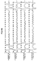
- the example shown in Fig. 7 is a simple matrix panel comprising 4 scanning electrodes 3 and 4 signal electrodes 4, which will be referred to as a 4 x 4 simple matrix panel (the former numeral indicating the number of the scanning electrodes 3 and the latter numeral indicating the number of the signal electrodes 4).
- the scanning electrodes 3 are labeled as L1, L2, L3 and L4 respectively, from the uppermost one, and the signal electrodes are labeled, from the left side, as S1, S2, S3 and S4, respectively.
- the intersection of the scanning electrode L i and the signal electrode S j is represented as a pixel A ij (i and j are positive integer).
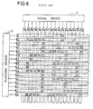
- Fig. 8 shows a 16 x 16 simple matrix panel displaying a letter " " ".
- Fig. 9 is a diagram of voltage waveforms applied to the scanning electrodes when the panel of Fig. 8 is driven.
- Fig. 10 is a diagram of voltage waveforms applied to the signal electrodes 4 for driving the panel shown in Fig. 8.
- Figs. 11A and 11B are diagrams of voltage waveforms applied to the pixels when the panel shown in Fig. 8 is driven.
- the operation for driving the panel shown in Fig. 8 in accordance with the conventional method of driving will be described in the following.
- the voltage shown in Fig. 9 is applied to the scanning electrode L i by the scanning driver 10, and the voltage shown in Fig. 10 is applied to the signal electrode S j by the signal driver 9.
- the voltages such as shown in Figs. 11A and 11B are applied to the pixel A ij , so that the pixel A ij is set in a bright or dark memory state, thereby displaying the character " " ".
- the ferroelectric liquid crystal has two memory states, one of which is referred to as the dark memory state while the other is referred to as the bright memory state.
- the bright memory state and the dark memory state maybe changed with each other.
- the voltage C (the voltage V0, and then the voltage -V0) is applied to the scanning electrodes L1 to L4 as shown in Fig. 9 (a) to (d), while the voltage G (voltage -2V0/3, and then the voltage 2V0/3) is applied to the scanning electrodes L5 to L9 as shown in Fig. 9 (e) to (h).
- the voltage A (voltage -V0 and then voltage V0) is applied to the scanning electrode L1 and the voltage B (voltage 2V0/3 and then the voltage -2V0/3) is applied to the remaining scanning electrodes.
- the voltage A is applied to the scanning electrode L2 and the voltage B is applied to the remaining scanning electrodes.
- the voltage A is applied to the scanning electrode L3 and the voltage B is applied to the remaining scanning electrodes.
- the voltage A is applied to the scanning electrode L4 and the voltage B is applied to the remaining scanning electrodes.
- the voltage C is applied to the scanning electrodes L5 to L8 and the voltage G is applied to the scanning electrode L9 and L1 to L4. Thereafter, the similar operation is repeated.
- the voltage F (voltage -V0 and then voltage V0) is applied to all the signal electrodes S j as shown in Fig. 10.
- the voltage D (voltage V0 and then the voltage -V0) or the voltage E (voltage V0/3 and then voltage -V0/3) is applied to each of the signal electrodes S j .
- the voltage F is applied to all the signal electrodes S j . Thereafter, the same operation is repeated.
- the voltages such as shown in Figs. 11A and 11B are applied to the pixels A ij . More specifically, the voltage applied to the pixel is equal to the voltage applied to the scanning electrode L i minus the voltage applied to the signal electrode S j .
- the voltage shown in Fig. 11A (a) is applied to the pixel A22.
- the voltage CF is applied to the pixels A 1j to A 4j including the pixel A22 during the time period -t0 to 0.
- the voltage 2V0 and then -2V0 are applied to the pixels including the pixel A22, which are set in the dark memory state.
- the ferroelectric liquid crystal sealed in this panel has a nature to be set in the dark memory state when the voltage -2V0 is applied for t0/2.
- the voltage A is supplied to the scanning electrode L2 and the voltage E is applied to the signal electrode S2 during the time period t0 to 2t0, then the voltage AE is applied to the pixel A22, keeping the dark memory state.
- the ferroelectric liquid crystal sealed in this panel has a nature that it is not set to the bright memory state even if the voltage 4V0/3 is applied for t0/2.
- the voltage shown in Fig. 11A (d) is applied to the pixel A 2c . Namely, the voltage CF is applied to the pixels A 1j to A 4j including the pixel A 2c during the time -t0 to 0.
- the voltage CF By the voltage CF, the voltage 2V0 and then -2V0 are applied to the pixels including the pixel A 2c , so that these pixels are set to the dark memory state. If the voltage A is applied to the scanning electrode L2 and the voltage D is applied to the signal electrode S c during t0 to 2t0, then the voltage AD is applied, so that the bright memory state is realized.
- the ferroelectric liquid crystal introduced in this panel has a nature that it is set to the bright memory state when the voltage 2V0 is applied for t0/2.
- the pixels A22 and A 2c rewritten in this manner are kept in the bright or dark memory state until the voltage CF is applied the next time as shown in Fig. 11A (a) and (d).
- the erasing voltage C and the non-selection voltage G are applied to a set of scanning electrodes 3, each set including 4 scanning electrodes 3.
- the erasing voltage C and the non-selection voltage G are applied to a set of scanning electrodes 3, each set including 2 to 16 electrodes.
- T a (17M ⁇ 16) x 2t m (sec)
- the scanning time per 1 scanning electrode provided by dividing the above value by the number of scanning electrodes m is about 2.1 x t m (sec).
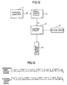
- Fig. 12 is a block diagram for the display of output signal of a conventional personal computer.
- Fig. 13 is a diagram of waveforms showing the output signal of the personal computer and the input signal of the signal driver showing in Fig. 12.
- the scanning time per scanning electrode can be made considerably close to 2t m (sec).
- a timing converting circuit 12 must be provided between the personal computer 11 and the control circuit 13 shown in Fig. 12. The reason for this is that although the output signal from the personal computer 11 is continues to the signal for the scanning electrodes L1, L2, L3, L4, L5, L6 and so on as shown in Fig. 13 (a), the actual signal to be applied to the signal driver 9 must include a signal corresponding to the timing of applying the voltage F to the signal electrode S j as shown in Fig. 13 (b). Therefore, the timing of the output signals of the personal computer 11 must be converted, so that they can be applied to the signal driver 9. See also GB-A-2 175 725.
- one object of the present invention is to provide a method of driving a ferroelectric liquid crystal displaying panel in a relatively simple manner without providing a timing converting circuit.
- the liquid crystal displaying panel comprises a plurality of scanning electrodes arranged parallel to each other, signal electrodes arranged parallel to each other intersecting the plurality of scanning electrodes, and ferroelectric liquid crystal sealed between the plurality of scanning electrodes and the plurality of signal electrodes.
- a compensation voltage G is applied followed by a succeeding erasing voltage H to the scanning electrode L i (i is a positive integer) corresponding to a pixel to be displayed out of the plurality of scanning electrodes, and thereafter a selecting voltage A is applied thereto, a bright voltage D is applied to a signal electrode corresponding to the pixel to be displayed, so that the corresponding pixel is turned on.
- the scanning time t0 per scanning electrode can be set twice the pulse width t m necessary for rewriting the memory state of the ferroelectric liquid crystal without providing the timing converting circuit as in the prior art.
- the compensation voltage G is a voltage which becomes negative for a prescribed time period
- the succeeding erasing voltage H is a voltage which becomes positive for a prescribed time period
- the selection voltage A is, in a former half of the predetermined time period, a negative voltage which is approximately equal to the succeeding erasing voltage H and, in the latter half of the period, a positive voltage which is approximately equal to the compensation voltage G
- the bright voltage D is, in the former half of the predetermined period, a positive voltage which is approximately the same as the selection voltage A in the latter half of the period, and in the latter half of the period, it is selected to be a negative voltage which is approximately equal to the selection voltage A in the former half of the period.
- a dark voltage E is applied to the signal electrode corresponding to the pixel to be displayed, so that the corresponding pixel is set in the off state.
- the dark voltage E is selected to be, in the former half of the prescribed period, a positive voltage lower than the bright voltage D in the former half of the period, and in the latter half, it is selected to be a negative voltage higher than the bright voltage D.
- the non-selection voltage B is applied to the scanning electrodes corresponding to the pixels which are not to be displayed, so that these pixels are set to the non-selected state.
- the non-selection voltage B is selected to be, in the former half in the predetermined time period, a positive voltage lower than the selection voltage A in the latter half and higher than the dark voltage E in the former half, and in the latter half of the period, a negative voltage higher than the selection voltage A in the former half and lower than the dark voltage E in the latter half.
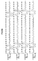
- Fig. 1 is a diagram of waveforms illustrating the principle of the present invention. Referring to Fig. 1, the principle of the present invention will be described. Before the selection voltage A is applied to the scanning electrode L i (i is a positive integer), the compensation voltage G is applied followed by the succeeding erasing voltage H. More specifically, from the time 0 to t0, a selection voltage A having the waveform as shown in Fig. 1 (1), that is, -V a in the former half of a predetermined time period and Va in the latter half of the period, is applied to the scanning electrode L i . A non-selection voltage B having such a waveform as shown in Fig.
- the succeeding erasing voltage H is applied to the scanning electrode L i .
- the voltage -V g - V d is applied in the former half of the period and the voltage -V g + V d is applied in the latter half of the period to the pixel A ij , as shown in Fig. 1 (g). If the dark voltage E shown in Fig.
- the pixel A ij can be kept in the dark memory state, since it is approximately the same as the application of the voltage -V g for the time P x t0 to the pixel A ij no matter whether the bright voltage D is applied or the dark voltage E is applied to the signal electrode S j .
- the compensation voltage G is applied. If the bright voltage D is applied to the signal electrode S j at this time, then, the voltage V g - V d is applied followed by the voltage V g + V d to the pixel A ij as shown in Fig. 1 (e).
- the voltage -V a is applied in the former half and the voltage V a is applied in the latter half as the selection voltage A
- the voltage V b is applied in the former half and the voltage -V b is applied in the latter half as the non-selection voltage B
- the voltage V g is applied as the compensation voltage G and the voltage -V g is applied as the succeeding erasing voltage H
- the voltage V d is applied in the former half and the voltage -V d is applied in the latter half as the bright voltage D
- the voltage V e is applied in the former half and the voltage -V e is applied in the latter half as the dark voltage E.
- the same effect can be obtained provided that the same voltage waveform is applied to the pixel A ij , even if the voltage V z or the like is commonly added to the respective voltages.
- Fig. 2 is a block diagram showing one embodiment of the present invention.
- a personal computer 11 a control circuit 13 a signal driver 9 and a scanning driver 10.
- the timing converting circuit 12 shown in Fig. 11 is omitted.
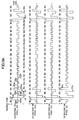
- Fig. 3 is a diagram of voltage waveforms applied to the scanning electrodes when the panel shown in Fig. 8 is driven.
- Fig. 4 is a diagram of voltage waveforms applied to the signal electrodes.
- Figs. 5A and 5B are diagrams of voltage waveforms applied to the pixels.
- a driving method of one embodiment of the present invention will be described in the following.
- the selection voltage A (voltage -V0 and then voltage V0) is applied to the scanning electrode L1; the succeeding erasing voltage H (voltage -V0) is applied to the scanning electrode L2; the compensation voltage G (voltage V0) is applied to the scanning electrode L3; and the non-selection voltage B (voltage 2V0/3 and then voltage -2V0/3) is applied to the scanning electrodes L4 to L9.
- the selection voltage A is applied to the scanning electrode L2
- the succeeding erasing voltage H is applied to the scanning electrode L3
- the compensation voltage G is applied to the scanning electrode L4
- the non-selection voltage B is applied to the scanning electrodes L5 to L9 and to L1.
- the dark voltage E (voltage V0/3 and then voltage -V0/3) or the bright voltage D (voltage V0 and then voltage -V0) is applied to the signal electrode S j .
- the voltages shown in Fig. 4 (a) to (e) are applied to the signal electrodes S2, S6, S b , S c and S d .
- the voltages applied to the pixels A22, A26, A 2b , A 2c , A 2d , A 3b , A32 and A36 are as shown in Fig. 5A (a) to (d) and Fig. 5B (e) to (h).
- the pixel A22 for example, is once set to the dark memory state by the difference voltage between the succeeding erasing voltage H and the dark voltage E or the bright voltage D, that is, HD or HE.
- the sealed ferroelectric liquid crystal is set to the dark memory state by the difference voltage HD as described with reference to the prior art. Approximately the same effect is provided by the difference voltage HE. In view of the variations of the characteristics of the cells, the succeeding erasing voltage H may be applied twice.
- the selection voltage A is applied from the time t0 to 2t0 to the scanning electrode L2.
- the dark voltage E must be applied to the signal electrode S j as shown in Fig. 4 (a) to (c).
- the difference voltage AE is applied to the pixel A 2j as shown in Fig. 5A (a) to (c).
- the memory state of the pixel A 2j is not changed, as shown in the prior art. If the pixel A 2j is to be set to the bright memory state, then the bright voltage D must be applied to the signal electrode S j as shown in Fig. 4 (d) and (e).
- the difference voltage AD is applied to the pixel A 2j as shown in Fig. 5A (d) and Fig. 5B (e) so that the pixel A 2j is changed to the bright memory state.
- a compensation voltage G and then the succeeding erasing voltage H are applied to the scanning electrode L1 before the application of the selection voltage A, so that the scanning time t0 (sec) per each scanning electrode can be set twice the time width t m (sec) of the pulse necessary for rewriting the memory state of the ferroelectric liquid crystal, without providing the timing conversion circuit as in the prior art.
Description
- The present invention relates to a method of driving a ferroelectric liquid crystal displaying panel. More specifically, the present invention relates to a method of driving a ferroelectric liquid crystal displaying panel having a plurality of scanning electrodes arranged parallel to each other, signal electrodes arranged parallel to each other intersecting the plurality of scanning electrodes and ferroelectric liquid crystal sealed between each of the scanning electrodes and each of the signal electrodes.
- Fig. 6 is a cross sectional view of a conventional simple matrix panel sealing ferroelectric liquid crystal. Referring to Fig. 6, two deflecting
plates 1 are provided at the top and bottom, arranged in the relation of crossed nicols with each other. Aglass 2 is provided on thedeflecting plate 1, and on whichglass 2 thescanning electrode 3 or thesignal electrode 4 is formed. Aninsulating film 5 is formed over thescanning electrodes 3 and thesignal electrodes 4 to protect the ferroelectricliquid crystal 8. An aligningfilm 6 is provided on theinsulating film 5 which is subjected to a process such as rubbing so as to align the molecules of theferroelectric liquid crystal 8.Sealing member 7 is provided for preventing the ferroelectric crystal liquid in the cell from leaking outward. - Fig. 7 shows the structure of the electrodes in the simple matrix panel sealing ferroelectric crystal liquid shown in Fig. 6. The example shown in Fig. 7 is a simple matrix panel comprising 4
scanning electrodes signal electrodes 4, which will be referred to as a 4 x 4 simple matrix panel (the former numeral indicating the number of thescanning electrodes 3 and the latter numeral indicating the number of the signal electrodes 4). Thescanning electrodes 3 are labeled as L₁, L₂, L₃ and L₄ respectively, from the uppermost one, and the signal electrodes are labeled, from the left side, as S₁, S₂, S₃ and S₄, respectively. The intersection of the scanning electrode Li and the signal electrode Sj is represented as a pixel Aij (i and j are positive integer). - Fig. 8 shows a 16 x 16 simple matrix panel displaying a letter "". Fig. 9 is a diagram of voltage waveforms applied to the scanning electrodes when the panel of Fig. 8 is driven. Fig. 10 is a diagram of voltage waveforms applied to the

signal electrodes 4 for driving the panel shown in Fig. 8. Figs. 11A and 11B are diagrams of voltage waveforms applied to the pixels when the panel shown in Fig. 8 is driven. - The operation for driving the panel shown in Fig. 8 in accordance with the conventional method of driving will be described in the following. The voltage shown in Fig. 9 is applied to the scanning electrode Li by the
scanning driver 10, and the voltage shown in Fig. 10 is applied to the signal electrode Sj by thesignal driver 9. Then, the voltages such as shown in Figs. 11A and 11B are applied to the pixel Aij, so that the pixel Aij is set in a bright or dark memory state, thereby displaying the character "".
- The ferroelectric liquid crystal has two memory states, one of which is referred to as the dark memory state while the other is referred to as the bright memory state. In the following, the bright memory state and the dark memory state maybe changed with each other.
- More specifically, as to the scanning electrodes Li, during the time period -t₀ to 0, the voltage C (the voltage V₀, and then the voltage -V₀) is applied to the scanning electrodes L₁ to L₄ as shown in Fig. 9 (a) to (d), while the voltage G (voltage -2V₀/3, and then the voltage 2V₀/3) is applied to the scanning electrodes L₅ to L₉ as shown in Fig. 9 (e) to (h). During the
time period 0 to t₀, the voltage A (voltage -V₀ and then voltage V₀) is applied to the scanning electrode L₁ and the voltage B (voltage 2V₀/3 and then the voltage -2V₀/3) is applied to the remaining scanning electrodes. - During the time t₀ to 2t₀, the voltage A is applied to the scanning electrode L₂ and the voltage B is applied to the remaining scanning electrodes. During the time period 2t₀ to 3t₀, the voltage A is applied to the scanning electrode L₃ and the voltage B is applied to the remaining scanning electrodes. During the time period 3t₀ to 4t₀, the voltage A is applied to the scanning electrode L₄ and the voltage B is applied to the remaining scanning electrodes. Then, during the time 4t₀ to 5t₀, the voltage C is applied to the scanning electrodes L₅ to L₈ and the voltage G is applied to the scanning electrode L₉ and L₁ to L₄. Thereafter, the similar operation is repeated.
- As to the signal electrodes Sj, during the time period -t₀ to 0, the voltage F (voltage -V₀ and then voltage V₀) is applied to all the signal electrodes Sj as shown in Fig. 10. During the
time period 0 to 4t₀, the voltage D (voltage V₀ and then the voltage -V₀) or the voltage E (voltage V₀/3 and then voltage -V₀/3) is applied to each of the signal electrodes Sj. During the time period 4t₀ to 5t₀, the voltage F is applied to all the signal electrodes Sj. Thereafter, the same operation is repeated. - By applying the voltages to the scanning electrodes L₁ to L₄ and L₅ to L₉ and to the signal electrodes Sj in the above described manner, the voltages such as shown in Figs. 11A and 11B are applied to the pixels Aij. More specifically, the voltage applied to the pixel is equal to the voltage applied to the scanning electrode Li minus the voltage applied to the signal electrode Sj. For example, the voltage shown in Fig. 11A (a) is applied to the pixel A₂₂. Namely, the voltage CF is applied to the pixels A1j to A4j including the pixel A₂₂ during the time period -t₀ to 0. By this voltage CF, the voltage 2V₀ and then -2V₀ are applied to the pixels including the pixel A₂₂, which are set in the dark memory state.
- The ferroelectric liquid crystal sealed in this panel has a nature to be set in the dark memory state when the voltage -2V₀ is applied for t₀/2. When the voltage A is supplied to the scanning electrode L₂ and the voltage E is applied to the signal electrode S₂ during the time period t₀ to 2t₀, then the voltage AE is applied to the pixel A₂₂, keeping the dark memory state. The ferroelectric liquid crystal sealed in this panel has a nature that it is not set to the bright memory state even if the voltage 4V₀/3 is applied for t₀/2. The voltage shown in Fig. 11A (d) is applied to the pixel A2c. Namely, the voltage CF is applied to the pixels A1j to A4j including the pixel A2c during the time -t₀ to 0. By the voltage CF, the voltage 2V₀ and then -2V₀ are applied to the pixels including the pixel A2c, so that these pixels are set to the dark memory state. If the voltage A is applied to the scanning electrode L₂ and the voltage D is applied to the signal electrode Sc during t₀ to 2t₀, then the voltage AD is applied, so that the bright memory state is realized. The ferroelectric liquid crystal introduced in this panel has a nature that it is set to the bright memory state when the voltage 2V₀ is applied for t₀/2.
- The pixels A₂₂ and A2c rewritten in this manner are kept in the bright or dark memory state until the voltage CF is applied the next time as shown in Fig. 11A (a) and (d).
- Since the example shown in Fig. 8 is a 16 x 16 simple matrix panel, the erasing voltage C and the non-selection voltage G are applied to a set of
scanning electrodes 3, each set including 4scanning electrodes 3. Generally, the erasing voltage C and the non-selection voltage G are applied to a set of scanningelectrodes 3, each set including 2 to 16 electrodes. When we represent the minimum panel time width necessary for rewriting the memory state of a ferroelectric liquid crystal with a certain applied voltage as tm (sec), then the time Ta necessary for rewriting all pixels in the M x N simple matrix panel will be as follows, when the erasing voltage C and the non-selection voltage G are applied to a set ofscanning electrodes 3 including 16 electrodes. - With a minimum integer K satisfying the condition of

the time Ta will be
- Assuming that M is a multiple of 16, then,

- Consequently, the scanning time per 1 scanning electrode provided by dividing the above value by the number of scanning electrodes m is about 2.1 x tm (sec).
- Fig. 12 is a block diagram for the display of output signal of a conventional personal computer. Fig. 13 is a diagram of waveforms showing the output signal of the personal computer and the input signal of the signal driver showing in Fig. 12.
- By using the above described method of driving, the scanning time per scanning electrode can be made considerably close to 2tm (sec). However, a
timing converting circuit 12 must be provided between thepersonal computer 11 and thecontrol circuit 13 shown in Fig. 12. The reason for this is that although the output signal from thepersonal computer 11 is continues to the signal for the scanning electrodes L₁, L₂, L₃, L₄, L₅, L₆ and so on as shown in Fig. 13 (a), the actual signal to be applied to thesignal driver 9 must include a signal corresponding to the timing of applying the voltage F to the signal electrode Sj as shown in Fig. 13 (b). Therefore, the timing of the output signals of thepersonal computer 11 must be converted, so that they can be applied to thesignal driver 9.
See also GB-A-2 175 725. - Therefore, one object of the present invention is to provide a method of driving a ferroelectric liquid crystal displaying panel in a relatively simple manner without providing a timing converting circuit.
- Briefly stated, in the present invention, the liquid crystal displaying panel comprises a plurality of scanning electrodes arranged parallel to each other, signal electrodes arranged parallel to each other intersecting the plurality of scanning electrodes, and ferroelectric liquid crystal sealed between the plurality of scanning electrodes and the plurality of signal electrodes. A compensation voltage G is applied followed by a succeeding erasing voltage H to the scanning electrode Li (i is a positive integer) corresponding to a pixel to be displayed out of the plurality of scanning electrodes, and thereafter a selecting voltage A is applied thereto, a bright voltage D is applied to a signal electrode corresponding to the pixel to be displayed, so that the corresponding pixel is turned on.
- Therefore, in accordance with the present invention, the scanning time t₀ per scanning electrode can be set twice the pulse width tm necessary for rewriting the memory state of the ferroelectric liquid crystal without providing the timing converting circuit as in the prior art.
- In accordance with a preferred embodiment of the present invention, the compensation voltage G is a voltage which becomes negative for a prescribed time period, the succeeding erasing voltage H is a voltage which becomes positive for a prescribed time period, the selection voltage A is, in a former half of the predetermined time period, a negative voltage which is approximately equal to the succeeding erasing voltage H and, in the latter half of the period, a positive voltage which is approximately equal to the compensation voltage G, the bright voltage D is, in the former half of the predetermined period, a positive voltage which is approximately the same as the selection voltage A in the latter half of the period, and in the latter half of the period, it is selected to be a negative voltage which is approximately equal to the selection voltage A in the former half of the period.
- In a more preferred embodiment, a dark voltage E is applied to the signal electrode corresponding to the pixel to be displayed, so that the corresponding pixel is set in the off state. The dark voltage E is selected to be, in the former half of the prescribed period, a positive voltage lower than the bright voltage D in the former half of the period, and in the latter half, it is selected to be a negative voltage higher than the bright voltage D.
- In a more preferred embodiment, the non-selection voltage B is applied to the scanning electrodes corresponding to the pixels which are not to be displayed, so that these pixels are set to the non-selected state. The non-selection voltage B is selected to be, in the former half in the predetermined time period, a positive voltage lower than the selection voltage A in the latter half and higher than the dark voltage E in the former half, and in the latter half of the period, a negative voltage higher than the selection voltage A in the former half and lower than the dark voltage E in the latter half.
- The foregoing and other objects, features, aspects and advantages of the present invention will become more apparent from the following detailed description of the present invention when taken in conjunction with the accompanying drawings.
-
- Fig. 1 is a diagram of voltage waveforms illustrating the principle of the present invention;
- Fig. 2 is a schematic block diagram of one embodiment of the present invention;
- Fig. 3 is a diagram of voltage waveforms applied to scanning electrodes in driving the liquid crystal display panel shown in Fig. 8;
- Fig. 4 is a diagram of voltage waveforms applied to signal electrodes in driving the panel shown in Fig. 8;
- Figs. 5A and 5B are diagrams of voltage waveforms applied to pixels in driving the liquid crystal display panel shown in Fig. 8;
- Fig. 6 is a cross sectional view of a conventional simple matrix panel sealing ferroelectric liquid crystal;
- Fig. 7 shows an electrode structure of the simple matrix panel sealing the ferroelectric liquid crystal shown in Fig. 6;
- Fig. 8 shows an example of a display of a letter "A" on a 16 x 16 matrix panel;
- Fig. 9 is a diagram of voltage waveforms applied to the scanning electrodes when the liquid crystal display panel shown in Fig. 8 is driven in a conventional manner;
- Fig. 10 is a diagram of voltage waveforms applied to the signal electrodes when the liquid crystal display panel of Fig. 8 is driven in the conventional manner;
- Figs. 11A and 11B are diagrams of voltage waveforms applied to the pixels when the panel shown in Fig. 8 is driven in the conventional manner;
- Fig. 12 is a schematic block diagram of a conventional apparatus for displaying output signals from a personal computer; and
- Fig. 13 shows output signals from the personal computer and the input signals of the signal driver shown in Fig. 12.
- Fig. 1 is a diagram of waveforms illustrating the principle of the present invention. Referring to Fig. 1, the principle of the present invention will be described. Before the selection voltage A is applied to the scanning electrode Li (i is a positive integer), the compensation voltage G is applied followed by the succeeding erasing voltage H. More specifically, from the
time 0 to t₀, a selection voltage A having the waveform as shown in Fig. 1 (1), that is, -Va in the former half of a predetermined time period and Va in the latter half of the period, is applied to the scanning electrode Li. A non-selection voltage B having such a waveform as shown in Fig. 1 (2), that is, the voltage Vb in the former half of the period and -Vb in the latter half of the period, or a compensation voltage G having such waveform as shown in Fig. 1 (3), that is, Vg in the predetermined period, or a succeeding erasing voltage H having such a waveform as shown in Fig. 1 (4), that is, -Vg in the prescribed time period, is applied to other scanning electrodes Lk (k ≠ i). - When a bright voltage D having the waveform as shown in Fig. 1 (5), that is, Vd in the former half of the period and -Vd in latter half of the period,is applied to the signal electrode Sj, then the pixel Aij corresponding to the scanning electrode Li is set to the bright memory state. When the dark voltage E having the waveform of Fig. 1 (6), that is, Ve in the former half of the period and -Ve and in the latter half of the period is applied, then the memory state of the pixel Aij corresponding to the scanning electrode Li is kept as it is.
- At the time P x t₀ (P= 1, 2...) before the application of the selection voltage A, the succeeding erasing voltage H is applied to the scanning electrode Li. When the bright voltage D is applied to the signal electrode Sj at this time, then the voltage -Vg - Vd is applied in the former half of the period and the voltage -Vg + Vd is applied in the latter half of the period to the pixel Aij, as shown in Fig. 1 (g). If the dark voltage E shown in Fig. 1 (6) is applied to the signal electrode Sj at this time, then the voltage -Vg - Ve is applied in the former half of the period and the voltage -Vg + Ve is applied in the latter half of the period to the pixel Aij as shown in Fig. 1 (h). Therefore, by determining the value of the voltage Vg such that -Vg + Vd ≦ 0 and -Vg + Ve ≦ 0, then the pixel Aij can be kept in the dark memory state, since it is approximately the same as the application of the voltage -Vg for the time P x t₀ to the pixel Aij no matter whether the bright voltage D is applied or the dark voltage E is applied to the signal electrode Sj.
- In addition, at the time Q x t₀ (Q= 1, 2...) before the application of the succeeding erasing voltage H to the scanning electrode Li, the compensation voltage G is applied. If the bright voltage D is applied to the signal electrode Sj at this time, then, the voltage Vg - Vd is applied followed by the voltage Vg + Vd to the pixel Aij as shown in Fig. 1 (e).
- When the dark voltage E is applied to the signal electrode Sj at this time, then the voltage Vg - Ve is applied followed by the voltage Vg + Ve to the pixel Aij as shown in Fig. 1 (f). Namely, no matter whether the bright voltage D is applied or the dark voltage E is applied to the electrode Sj, an average voltage of V g is applied for the time Q x t₀ to the pixel Aij. Therefore, by applying the succeeding erasing voltage H to the scanning electrode Li and by applying the compensation voltage G to the signal electrode Sj, the voltage time product Vg x P x t₀ applied to the pixel Aij is cancelled, realizing driving with no DC component left therein.
- The voltage -Va is applied in the former half and the voltage Va is applied in the latter half as the selection voltage A, the voltage Vb is applied in the former half and the voltage -Vb is applied in the latter half as the non-selection voltage B, the voltage Vg is applied as the compensation voltage G and the voltage -Vg is applied as the succeeding erasing voltage H, the voltage Vd is applied in the former half and the voltage -Vd is applied in the latter half as the bright voltage D and the voltage Ve is applied in the former half and the voltage -Ve is applied in the latter half as the dark voltage E. However, the same effect can be obtained provided that the same voltage waveform is applied to the pixel Aij, even if the voltage Vz or the like is commonly added to the respective voltages.
- Fig. 2 is a block diagram showing one embodiment of the present invention. In this embodiment, provided are a
personal computer 11, acontrol circuit 13, asignal driver 9 and ascanning driver 10. Thetiming converting circuit 12 shown in Fig. 11 is omitted. - In this embodiment also, the simple matrix panel shown in Fig. 8 is driven.
- Fig. 3 is a diagram of voltage waveforms applied to the scanning electrodes when the panel shown in Fig. 8 is driven. Fig. 4 is a diagram of voltage waveforms applied to the signal electrodes. Figs. 5A and 5B are diagrams of voltage waveforms applied to the pixels.
- A driving method of one embodiment of the present invention will be described in the following. As shown in Fig. 3 (a) to (d), from the
time 0 to t₀, the selection voltage A (voltage -V₀ and then voltage V₀) is applied to the scanning electrode L₁; the succeeding erasing voltage H (voltage -V₀) is applied to the scanning electrode L₂; the compensation voltage G (voltage V₀) is applied to the scanning electrode L₃; and the non-selection voltage B (voltage 2V₀/3 and then voltage -2V₀/3) is applied to the scanning electrodes L₄ to L₉. Then, from the time t₀ to 2t₀, the selection voltage A is applied to the scanning electrode L₂, the succeeding erasing voltage H is applied to the scanning electrode L₃, the compensation voltage G is applied to the scanning electrode L₄, and the non-selection voltage B is applied to the scanning electrodes L₅ to L₉ and to L₁. - While the scanning electrodes L₁ to L₉ are scanned in this manner, the dark voltage E (voltage V₀/3 and then voltage -V₀/3) or the bright voltage D (voltage V₀ and then voltage -V₀) is applied to the signal electrode Sj. In order to display the letter "A" as shown in Fig. 8, the voltages shown in Fig. 4 (a) to (e) are applied to the signal electrodes S₂, S₆, Sb, Sc and Sd.
- Consequently, the voltages applied to the pixels A₂₂, A₂₆, A2b, A2c, A2d, A3b, A₃₂ and A₃₆ are as shown in Fig. 5A (a) to (d) and Fig. 5B (e) to (h). The pixel A₂₂, for example, is once set to the dark memory state by the difference voltage between the succeeding erasing voltage H and the dark voltage E or the bright voltage D, that is, HD or HE.
- The sealed ferroelectric liquid crystal is set to the dark memory state by the difference voltage HD as described with reference to the prior art. Approximately the same effect is provided by the difference voltage HE. In view of the variations of the characteristics of the cells, the succeeding erasing voltage H may be applied twice.
- The selection voltage A is applied from the time t₀ to 2t₀ to the scanning electrode L₂. When the pixel A2j is to be set to the dark memory state on this occasion, then the dark voltage E must be applied to the signal electrode Sj as shown in Fig. 4 (a) to (c).
- At this time, the difference voltage AE is applied to the pixel A2j as shown in Fig. 5A (a) to (c). However, the memory state of the pixel A2j is not changed, as shown in the prior art. If the pixel A2j is to be set to the bright memory state, then the bright voltage D must be applied to the signal electrode Sj as shown in Fig. 4 (d) and (e). On this occasion, the difference voltage AD is applied to the pixel A2j as shown in Fig. 5A (d) and Fig. 5B (e) so that the pixel A2j is changed to the bright memory state. In practice, CS - 1014 produced by CHISSO Corp. is sealed in the simple matrix panel as the ferroelectric liquid crystal and it is driven with


- As described above, in this embodiment of the present invention, a compensation voltage G and then the succeeding erasing voltage H are applied to the scanning electrode L₁ before the application of the selection voltage A, so that the scanning time t₀ (sec) per each scanning electrode can be set twice the time width tm (sec) of the pulse necessary for rewriting the memory state of the ferroelectric liquid crystal, without providing the timing conversion circuit as in the prior art.
- Although the present invention has been described and illustrated in detail, it is clearly understood that the same is by way of illustration and example only and is not to be taken by way of limitation, the scope of the present invention being limited only by the terms of the appended claims.
Claims (9)
- A method of driving a liquid crystal display panel having a plurality of scanning electrodes (Li, i is a positive integer) arranged parallel to each other, a plurality of signal electrodes (Sj, j is a positive integer) arranged parallel to each other and intersecting said plurality of said scanning electrodes, and ferroelectric liquid crystal (8) sealed between said plurality of scanning electrodes and the plurality of signal electrodes, comprising the steps of:
applying a compensation voltage (G) followed by a succeeding erasing voltage (H) and thereafter applying a selection voltage (A) to a selected scanning electrode (Li) corresponding to a pixel to be displayed out of said plurality of scanning electrodes; and
applying a bright voltage (D) to a signal electrode corresponding to said pixel to be displayed; whereby the corresponding pixel is turned on. - A method of driving a ferroelectric liquid crystal display panel according to claim 1, wherein said succeeding erasing voltage (H) has a pulse width of at least twice the duration of a pulse width of said selection voltage (A), such that by applying said succeeding erasing voltage (H) having the same magnitude as said selection voltage (A) to said scanning electrode (Li) said corresponding pixel can be erased prior to applying said selection voltage (A) to said scanning electrode (Li).
- A method of driving a ferroelectric liquid crystal display panel according to claim 1 or claim 2, wherein:
said compensation voltage (G) comprises a voltage which becomes negative for a prescribed time period,
said succeeding erasing voltage (H) comprises a voltage which becomes positive for said predetermined time period;
said selection voltage (A) comprises, in the former half of said predetermined time period, a negative voltage approximately equal to the succeeding erasing voltage (H) and, in the latter half of said predetermined time period, a positive voltage approximately equal to said compensation voltage (G); and
said bright voltage (D) comprises, in the former half of said predetermined time period, a positive voltage approximately equal to said selection voltage (A) in the latter half of the period, and in the latter half of the period, a negative voltage approximately equal to said selection voltage (A) in the former half of the period. - A method of driving a ferroelectric liquid crystal display panel according to claim 3, further comprising the step of:
applying a dark voltage (E) to the signal electrode corresponding to said pixel to be displayed, whereby the corresponding pixel is turned off. - A method of driving a ferroelectric liquid crystal display panel according to claim 4, wherein:
said dark voltage (E) comprises, the former half of said predetermined period, a positive voltage lower than said bright voltage (D) in the former half of the period, and, in the latter half of the period, a negative voltage higher than said bright voltage (D) in the latter half of the period. - A method of driving a ferroelectric liquid crystal display panel according to claim 5, further comprising the step of:
applying a non-selection voltage (B) to the scanning electrodes other than the selected scanning electrode. - A method of driving a ferroelectric liquid crystal display panel according to claim 6, wherein:
said non-selection voltage (B) comprises, in the former half of said predetermined period, a positive voltage lower than said selection voltage (A) in the latter half of the period and higher than said dark voltage (E) in the former half of the period, and in the latter half of the period, a negative voltage higher than said selection voltage (A) in the former half of the period and lower than said dark voltage (E) in the latter half of the period. - Liquid crystal matrix display drive circuit in which an erasing voltage (H) applied to a scanning electrode prior to the selection thereof by a selection voltage (A) is preceded by a compensation voltage (G) applied to that scanning electrode.
- A drive circuit for driving a liquid crystal display panel by a method according to any one of claims 1 to 7.
Applications Claiming Priority (2)
| Application Number | Priority Date | Filing Date | Title |
|---|---|---|---|
| JP63278139A JPH02123327A (en) | 1988-11-01 | 1988-11-01 | Driving method for ferroelectric liquid crystal |
| JP278139/88 | 1988-11-01 |
Publications (3)
| Publication Number | Publication Date |
|---|---|
| EP0367531A2 EP0367531A2 (en) | 1990-05-09 |
| EP0367531A3 EP0367531A3 (en) | 1992-01-22 |
| EP0367531B1 true EP0367531B1 (en) | 1994-12-14 |
Family
ID=17593132
Family Applications (1)
| Application Number | Title | Priority Date | Filing Date |
|---|---|---|---|
| EP89311174A Expired - Lifetime EP0367531B1 (en) | 1988-11-01 | 1989-10-30 | Method of driving ferroelectric liquid crystal display panel |
Country Status (4)
| Country | Link |
|---|---|
| US (1) | US5048934A (en) |
| EP (1) | EP0367531B1 (en) |
| JP (1) | JPH02123327A (en) |
| DE (1) | DE68920002T2 (en) |
Families Citing this family (8)
| Publication number | Priority date | Publication date | Assignee | Title |
|---|---|---|---|---|
| JP3143497B2 (en) * | 1990-08-22 | 2001-03-07 | キヤノン株式会社 | Liquid crystal device |
| US5283564A (en) * | 1990-12-26 | 1994-02-01 | Canon Kabushiki Kaisha | Liquid crystal apparatus with temperature-dependent pulse manipulation |
| JP3482667B2 (en) * | 1993-01-13 | 2003-12-22 | セイコーエプソン株式会社 | Driving method of liquid crystal display device and liquid crystal display device |
| US6271817B1 (en) | 1991-03-20 | 2001-08-07 | Seiko Epson Corporation | Method of driving liquid crystal display device that reduces afterimages |
| JP2954429B2 (en) * | 1992-08-25 | 1999-09-27 | シャープ株式会社 | Active matrix drive |
| JP3229156B2 (en) * | 1995-03-15 | 2001-11-12 | 株式会社東芝 | Liquid crystal display |
| JP3688574B2 (en) | 1999-10-08 | 2005-08-31 | シャープ株式会社 | Liquid crystal display device and light source device |
| JP4076451B2 (en) | 2003-01-28 | 2008-04-16 | トピー工業株式会社 | Rim material for unequal thickness rim, unequal thickness rim, manufacturing method of unequal thickness rim |
Family Cites Families (13)
| Publication number | Priority date | Publication date | Assignee | Title |
|---|---|---|---|---|
| US4878741A (en) * | 1986-09-10 | 1989-11-07 | Manchester R & D Partnership | Liquid crystal color display and method |
| GB2175725B (en) * | 1985-04-04 | 1989-10-25 | Seikosha Kk | Improvements in or relating to electro-optical display devices |
| JPH0695179B2 (en) * | 1985-09-06 | 1994-11-24 | 松下電器産業株式会社 | Driving method of liquid crystal matrix display panel |
| SE8504760D0 (en) * | 1985-10-14 | 1985-10-14 | Sven Torbjorn Lagerwall | ELECTRONIC ADDRESSING OF FERROELECTRIC LIQUID CRYSTAL DEVICES |
| JPS62141520A (en) * | 1985-12-16 | 1987-06-25 | Casio Comput Co Ltd | Liquid crystal driving method |
| JPH0827601B2 (en) * | 1986-01-13 | 1996-03-21 | 株式会社日立製作所 | Liquid crystal display device and driving method thereof |
| US4903875A (en) * | 1986-05-20 | 1990-02-27 | Smart Peter E | Ski-carrying device |
| JPS6311912A (en) * | 1986-07-02 | 1988-01-19 | Mitsubishi Electric Corp | Driving device for liquid-crystal display device |
| JP2823049B2 (en) * | 1986-08-13 | 1998-11-11 | キヤノン株式会社 | 2D display |
| DE3784809T2 (en) * | 1986-08-18 | 1993-07-08 | Canon Kk | METHOD AND DEVICE FOR CONTROLLING AN OPTICAL MODULATION ARRANGEMENT. |
| JPS6373228A (en) * | 1986-09-17 | 1988-04-02 | Canon Inc | Method for driving optical modulating element |
| JP2565925B2 (en) * | 1987-09-29 | 1996-12-18 | 株式会社東芝 | Matrix drive display |
| US4922240A (en) * | 1987-12-29 | 1990-05-01 | North American Philips Corp. | Thin film active matrix and addressing circuitry therefor |
-
1988
- 1988-11-01 JP JP63278139A patent/JPH02123327A/en active Pending
-
1989
- 1989-10-25 US US07/426,171 patent/US5048934A/en not_active Expired - Lifetime
- 1989-10-30 EP EP89311174A patent/EP0367531B1/en not_active Expired - Lifetime
- 1989-10-30 DE DE68920002T patent/DE68920002T2/en not_active Expired - Fee Related
Also Published As
| Publication number | Publication date |
|---|---|
| US5048934A (en) | 1991-09-17 |
| EP0367531A3 (en) | 1992-01-22 |
| EP0367531A2 (en) | 1990-05-09 |
| DE68920002D1 (en) | 1995-01-26 |
| DE68920002T2 (en) | 1995-06-22 |
| JPH02123327A (en) | 1990-05-10 |
Similar Documents
| Publication | Publication Date | Title |
|---|---|---|
| US5940057A (en) | Method and apparatus for eliminating crosstalk in active matrix liquid crystal displays | |
| EP0366117B1 (en) | Liquid crystal apparatus | |
| EP0391655B1 (en) | A drive device for driving a matrix-type LCD apparatus | |
| US5033822A (en) | Liquid crystal apparatus with temperature compensation control circuit | |
| US6600465B1 (en) | Driver circuit for active matrix display | |
| EP0623911A1 (en) | Method for driving liquid crystal display device | |
| EP0256548A1 (en) | Method and apparatus for driving optical modulation device | |
| US5838293A (en) | Driving method and system for antiferroelectric liquid-crystal display device | |
| AU7424291A (en) | Liquid crystal display apparatus and driving method of such apparatus | |
| US7215310B2 (en) | Liquid crystal display device | |
| JP2954429B2 (en) | Active matrix drive | |
| US4925277A (en) | Method and apparatus for driving optical modulation device | |
| EP0367531B1 (en) | Method of driving ferroelectric liquid crystal display panel | |
| JP3034612B2 (en) | Matrix type LCD panel addressing method | |
| EP0503321B1 (en) | Liquid crystal display apparatus | |
| US20010022567A1 (en) | Display device | |
| JP2003029719A (en) | Liquid crystal display device | |
| EP0706169A1 (en) | Method of displaying gray scales on a ferroelectric liquid crystal cell with variable thickness | |
| JP2575189B2 (en) | Liquid crystal device | |
| EP0544427B1 (en) | Display module drive circuit having a digital source driver capable of generating multi-level drive voltages from a single external power source | |
| JP2002072974A (en) | Method for driving liquid crystal display device | |
| EP0293235B1 (en) | Display device and driving system thereof | |
| EP0221613A1 (en) | Low drive voltage display device | |
| EP0492542B1 (en) | Method of display control | |
| JPH04118625A (en) | Driving circuit of liquid crystal display device |
Legal Events
| Date | Code | Title | Description |
|---|---|---|---|
| PUAI | Public reference made under article 153(3) epc to a published international application that has entered the european phase |
Free format text: ORIGINAL CODE: 0009012 |
|
| AK | Designated contracting states |
Kind code of ref document: A2 Designated state(s): DE FR GB |
|
| 17P | Request for examination filed |
Effective date: 19901214 |
|
| PUAL | Search report despatched |
Free format text: ORIGINAL CODE: 0009013 |
|
| AK | Designated contracting states |
Kind code of ref document: A3 Designated state(s): DE FR GB |
|
| 17Q | First examination report despatched |
Effective date: 19940223 |
|
| GRAA | (expected) grant |
Free format text: ORIGINAL CODE: 0009210 |
|
| AK | Designated contracting states |
Kind code of ref document: B1 Designated state(s): DE FR GB |
|
| REF | Corresponds to: |
Ref document number: 68920002 Country of ref document: DE Date of ref document: 19950126 |
|
| ET | Fr: translation filed | ||
| PLBE | No opposition filed within time limit |
Free format text: ORIGINAL CODE: 0009261 |
|
| STAA | Information on the status of an ep patent application or granted ep patent |
Free format text: STATUS: NO OPPOSITION FILED WITHIN TIME LIMIT |
|
| 26N | No opposition filed | ||
| REG | Reference to a national code |
Ref country code: GB Ref legal event code: IF02 |
|
| PGFP | Annual fee paid to national office [announced via postgrant information from national office to epo] |
Ref country code: FR Payment date: 20041008 Year of fee payment: 16 |
|
| PGFP | Annual fee paid to national office [announced via postgrant information from national office to epo] |
Ref country code: GB Payment date: 20041027 Year of fee payment: 16 |
|
| PGFP | Annual fee paid to national office [announced via postgrant information from national office to epo] |
Ref country code: DE Payment date: 20041028 Year of fee payment: 16 |
|
| PG25 | Lapsed in a contracting state [announced via postgrant information from national office to epo] |
Ref country code: GB Free format text: LAPSE BECAUSE OF NON-PAYMENT OF DUE FEES Effective date: 20051030 |
|
| PG25 | Lapsed in a contracting state [announced via postgrant information from national office to epo] |
Ref country code: DE Free format text: LAPSE BECAUSE OF NON-PAYMENT OF DUE FEES Effective date: 20060503 |
|
| GBPC | Gb: european patent ceased through non-payment of renewal fee |
Effective date: 20051030 |
|
| PG25 | Lapsed in a contracting state [announced via postgrant information from national office to epo] |
Ref country code: FR Free format text: LAPSE BECAUSE OF NON-PAYMENT OF DUE FEES Effective date: 20060630 |
|
| REG | Reference to a national code |
Ref country code: FR Ref legal event code: ST Effective date: 20060630 |