EP0366117B1 - Liquid crystal apparatus - Google Patents
Liquid crystal apparatus Download PDFInfo
- Publication number
- EP0366117B1 EP0366117B1 EP89119844A EP89119844A EP0366117B1 EP 0366117 B1 EP0366117 B1 EP 0366117B1 EP 89119844 A EP89119844 A EP 89119844A EP 89119844 A EP89119844 A EP 89119844A EP 0366117 B1 EP0366117 B1 EP 0366117B1
- Authority
- EP
- European Patent Office
- Prior art keywords
- scanning
- electrodes
- voltage
- liquid crystal
- selection signal
- Prior art date
- Legal status (The legal status is an assumption and is not a legal conclusion. Google has not performed a legal analysis and makes no representation as to the accuracy of the status listed.)
- Expired - Lifetime
Links
- 239000004973 liquid crystal related substance Substances 0.000 title claims abstract description 45
- 239000005262 ferroelectric liquid crystals (FLCs) Substances 0.000 claims abstract description 71
- 239000011159 matrix material Substances 0.000 claims abstract description 20
- 230000000694 effects Effects 0.000 claims abstract description 5
- 230000015654 memory Effects 0.000 description 18
- 238000010586 diagram Methods 0.000 description 12
- 238000000034 method Methods 0.000 description 12
- 239000000872 buffer Substances 0.000 description 5
- 230000005684 electric field Effects 0.000 description 5
- 239000003086 colorant Substances 0.000 description 3
- 230000000717 retained effect Effects 0.000 description 3
- 230000000295 complement effect Effects 0.000 description 2
- 238000013479 data entry Methods 0.000 description 2
- 230000003287 optical effect Effects 0.000 description 2
- 239000010409 thin film Substances 0.000 description 2
- 239000004990 Smectic liquid crystal Substances 0.000 description 1
- 229910021417 amorphous silicon Inorganic materials 0.000 description 1
- 239000003990 capacitor Substances 0.000 description 1
- 230000008859 change Effects 0.000 description 1
- 239000013078 crystal Substances 0.000 description 1
- 230000003247 decreasing effect Effects 0.000 description 1
- 230000006870 function Effects 0.000 description 1
- 239000011521 glass Substances 0.000 description 1
- 230000006872 improvement Effects 0.000 description 1
- 239000000463 material Substances 0.000 description 1
- 230000003446 memory effect Effects 0.000 description 1
- 230000006386 memory function Effects 0.000 description 1
- 230000010287 polarization Effects 0.000 description 1
- 229910021420 polycrystalline silicon Inorganic materials 0.000 description 1
- 229920005591 polysilicon Polymers 0.000 description 1
- 230000004044 response Effects 0.000 description 1
- 239000004065 semiconductor Substances 0.000 description 1
- 239000000758 substrate Substances 0.000 description 1
- 230000001629 suppression Effects 0.000 description 1
Images


Classifications
-
- G—PHYSICS
- G09—EDUCATION; CRYPTOGRAPHY; DISPLAY; ADVERTISING; SEALS
- G09G—ARRANGEMENTS OR CIRCUITS FOR CONTROL OF INDICATING DEVICES USING STATIC MEANS TO PRESENT VARIABLE INFORMATION
- G09G3/00—Control arrangements or circuits, of interest only in connection with visual indicators other than cathode-ray tubes
- G09G3/20—Control arrangements or circuits, of interest only in connection with visual indicators other than cathode-ray tubes for presentation of an assembly of a number of characters, e.g. a page, by composing the assembly by combination of individual elements arranged in a matrix no fixed position being assigned to or needed to be assigned to the individual characters or partial characters
- G09G3/34—Control arrangements or circuits, of interest only in connection with visual indicators other than cathode-ray tubes for presentation of an assembly of a number of characters, e.g. a page, by composing the assembly by combination of individual elements arranged in a matrix no fixed position being assigned to or needed to be assigned to the individual characters or partial characters by control of light from an independent source
- G09G3/36—Control arrangements or circuits, of interest only in connection with visual indicators other than cathode-ray tubes for presentation of an assembly of a number of characters, e.g. a page, by composing the assembly by combination of individual elements arranged in a matrix no fixed position being assigned to or needed to be assigned to the individual characters or partial characters by control of light from an independent source using liquid crystals
- G09G3/3611—Control of matrices with row and column drivers
- G09G3/3622—Control of matrices with row and column drivers using a passive matrix
- G09G3/3629—Control of matrices with row and column drivers using a passive matrix using liquid crystals having memory effects, e.g. ferroelectric liquid crystals
-
- G—PHYSICS
- G09—EDUCATION; CRYPTOGRAPHY; DISPLAY; ADVERTISING; SEALS
- G09G—ARRANGEMENTS OR CIRCUITS FOR CONTROL OF INDICATING DEVICES USING STATIC MEANS TO PRESENT VARIABLE INFORMATION
- G09G3/00—Control arrangements or circuits, of interest only in connection with visual indicators other than cathode-ray tubes
- G09G3/20—Control arrangements or circuits, of interest only in connection with visual indicators other than cathode-ray tubes for presentation of an assembly of a number of characters, e.g. a page, by composing the assembly by combination of individual elements arranged in a matrix no fixed position being assigned to or needed to be assigned to the individual characters or partial characters
- G09G3/34—Control arrangements or circuits, of interest only in connection with visual indicators other than cathode-ray tubes for presentation of an assembly of a number of characters, e.g. a page, by composing the assembly by combination of individual elements arranged in a matrix no fixed position being assigned to or needed to be assigned to the individual characters or partial characters by control of light from an independent source
- G09G3/36—Control arrangements or circuits, of interest only in connection with visual indicators other than cathode-ray tubes for presentation of an assembly of a number of characters, e.g. a page, by composing the assembly by combination of individual elements arranged in a matrix no fixed position being assigned to or needed to be assigned to the individual characters or partial characters by control of light from an independent source using liquid crystals
- G09G3/3607—Control arrangements or circuits, of interest only in connection with visual indicators other than cathode-ray tubes for presentation of an assembly of a number of characters, e.g. a page, by composing the assembly by combination of individual elements arranged in a matrix no fixed position being assigned to or needed to be assigned to the individual characters or partial characters by control of light from an independent source using liquid crystals for displaying colours or for displaying grey scales with a specific pixel layout, e.g. using sub-pixels
-
- G—PHYSICS
- G09—EDUCATION; CRYPTOGRAPHY; DISPLAY; ADVERTISING; SEALS
- G09G—ARRANGEMENTS OR CIRCUITS FOR CONTROL OF INDICATING DEVICES USING STATIC MEANS TO PRESENT VARIABLE INFORMATION
- G09G3/00—Control arrangements or circuits, of interest only in connection with visual indicators other than cathode-ray tubes
- G09G3/20—Control arrangements or circuits, of interest only in connection with visual indicators other than cathode-ray tubes for presentation of an assembly of a number of characters, e.g. a page, by composing the assembly by combination of individual elements arranged in a matrix no fixed position being assigned to or needed to be assigned to the individual characters or partial characters
- G09G3/34—Control arrangements or circuits, of interest only in connection with visual indicators other than cathode-ray tubes for presentation of an assembly of a number of characters, e.g. a page, by composing the assembly by combination of individual elements arranged in a matrix no fixed position being assigned to or needed to be assigned to the individual characters or partial characters by control of light from an independent source
- G09G3/36—Control arrangements or circuits, of interest only in connection with visual indicators other than cathode-ray tubes for presentation of an assembly of a number of characters, e.g. a page, by composing the assembly by combination of individual elements arranged in a matrix no fixed position being assigned to or needed to be assigned to the individual characters or partial characters by control of light from an independent source using liquid crystals
- G09G3/3611—Control of matrices with row and column drivers
- G09G3/3622—Control of matrices with row and column drivers using a passive matrix
- G09G3/3629—Control of matrices with row and column drivers using a passive matrix using liquid crystals having memory effects, e.g. ferroelectric liquid crystals
- G09G3/364—Control of matrices with row and column drivers using a passive matrix using liquid crystals having memory effects, e.g. ferroelectric liquid crystals with use of subpixels
-
- G—PHYSICS
- G09—EDUCATION; CRYPTOGRAPHY; DISPLAY; ADVERTISING; SEALS
- G09G—ARRANGEMENTS OR CIRCUITS FOR CONTROL OF INDICATING DEVICES USING STATIC MEANS TO PRESENT VARIABLE INFORMATION
- G09G3/00—Control arrangements or circuits, of interest only in connection with visual indicators other than cathode-ray tubes
- G09G3/20—Control arrangements or circuits, of interest only in connection with visual indicators other than cathode-ray tubes for presentation of an assembly of a number of characters, e.g. a page, by composing the assembly by combination of individual elements arranged in a matrix no fixed position being assigned to or needed to be assigned to the individual characters or partial characters
- G09G3/34—Control arrangements or circuits, of interest only in connection with visual indicators other than cathode-ray tubes for presentation of an assembly of a number of characters, e.g. a page, by composing the assembly by combination of individual elements arranged in a matrix no fixed position being assigned to or needed to be assigned to the individual characters or partial characters by control of light from an independent source
- G09G3/36—Control arrangements or circuits, of interest only in connection with visual indicators other than cathode-ray tubes for presentation of an assembly of a number of characters, e.g. a page, by composing the assembly by combination of individual elements arranged in a matrix no fixed position being assigned to or needed to be assigned to the individual characters or partial characters by control of light from an independent source using liquid crystals
- G09G3/3611—Control of matrices with row and column drivers
- G09G3/3674—Details of drivers for scan electrodes
-
- G—PHYSICS
- G09—EDUCATION; CRYPTOGRAPHY; DISPLAY; ADVERTISING; SEALS
- G09G—ARRANGEMENTS OR CIRCUITS FOR CONTROL OF INDICATING DEVICES USING STATIC MEANS TO PRESENT VARIABLE INFORMATION
- G09G2310/00—Command of the display device
- G09G2310/02—Addressing, scanning or driving the display screen or processing steps related thereto
- G09G2310/0224—Details of interlacing
- G09G2310/0227—Details of interlacing related to multiple interlacing, i.e. involving more fields than just one odd field and one even field
-
- G—PHYSICS
- G09—EDUCATION; CRYPTOGRAPHY; DISPLAY; ADVERTISING; SEALS
- G09G—ARRANGEMENTS OR CIRCUITS FOR CONTROL OF INDICATING DEVICES USING STATIC MEANS TO PRESENT VARIABLE INFORMATION
- G09G2310/00—Command of the display device
- G09G2310/06—Details of flat display driving waveforms
-
- G—PHYSICS
- G09—EDUCATION; CRYPTOGRAPHY; DISPLAY; ADVERTISING; SEALS
- G09G—ARRANGEMENTS OR CIRCUITS FOR CONTROL OF INDICATING DEVICES USING STATIC MEANS TO PRESENT VARIABLE INFORMATION
- G09G2310/00—Command of the display device
- G09G2310/06—Details of flat display driving waveforms
- G09G2310/065—Waveforms comprising zero voltage phase or pause
-
- G—PHYSICS
- G09—EDUCATION; CRYPTOGRAPHY; DISPLAY; ADVERTISING; SEALS
- G09G—ARRANGEMENTS OR CIRCUITS FOR CONTROL OF INDICATING DEVICES USING STATIC MEANS TO PRESENT VARIABLE INFORMATION
- G09G2320/00—Control of display operating conditions
- G09G2320/04—Maintaining the quality of display appearance
- G09G2320/041—Temperature compensation
-
- G—PHYSICS
- G09—EDUCATION; CRYPTOGRAPHY; DISPLAY; ADVERTISING; SEALS
- G09G—ARRANGEMENTS OR CIRCUITS FOR CONTROL OF INDICATING DEVICES USING STATIC MEANS TO PRESENT VARIABLE INFORMATION
- G09G3/00—Control arrangements or circuits, of interest only in connection with visual indicators other than cathode-ray tubes
- G09G3/20—Control arrangements or circuits, of interest only in connection with visual indicators other than cathode-ray tubes for presentation of an assembly of a number of characters, e.g. a page, by composing the assembly by combination of individual elements arranged in a matrix no fixed position being assigned to or needed to be assigned to the individual characters or partial characters
- G09G3/2007—Display of intermediate tones
- G09G3/2018—Display of intermediate tones by time modulation using two or more time intervals
-
- G—PHYSICS
- G09—EDUCATION; CRYPTOGRAPHY; DISPLAY; ADVERTISING; SEALS
- G09G—ARRANGEMENTS OR CIRCUITS FOR CONTROL OF INDICATING DEVICES USING STATIC MEANS TO PRESENT VARIABLE INFORMATION
- G09G3/00—Control arrangements or circuits, of interest only in connection with visual indicators other than cathode-ray tubes
- G09G3/20—Control arrangements or circuits, of interest only in connection with visual indicators other than cathode-ray tubes for presentation of an assembly of a number of characters, e.g. a page, by composing the assembly by combination of individual elements arranged in a matrix no fixed position being assigned to or needed to be assigned to the individual characters or partial characters
- G09G3/2007—Display of intermediate tones
- G09G3/2074—Display of intermediate tones using sub-pixels
Definitions
- the present invention relates to a display apparatus using a ferroelectric liquid crystal, particularly a liquid crystal apparatus free from occurrence of noticeable flicker.
- TFT thin film transistors
- a gradational display is performed in such a manner that a TFT is supplied with a gate-on pulse to make the source and drain conductive between each other, an image signal is supplied through the source at that time to be stored in a capacitor, and a liquid crystal (e.g., a twisted nematic (TN) liquid crystal) at the pixel is driven corresponding to the stored signal while modulating the voltage of the image signal.
- TN twisted nematic
- each TFT used has a complicated structure requiring many steps for production, so that a high production cost is incurred and also it is difficult to form a thin film semiconductor of, e.g., polysilicon or amorphous silicon constituting TFTs over a wide area.
- a display panel of the passive matrix system using a TN-liquid crystal has been known as one which can be attained at a low production cost.
- a duty ratio i.e., a ratio of time wherein a selected point is supplied with an effective electric field during scanning of one picture (one frame)
- N the number of scanning lines
- this type of liquid crystal panel is not suitable as a display panel with a high density of lines, particularly as a liquid crystal television panel.
- a ferroelectric liquid crystal (hereinafter sometimes abbreviated as "FLC") showing chiral smectic C phase (SmC*) or H phase (SmH*) is generally used.
- FLC ferroelectric liquid crystal
- the ferroelectric liquid crystal assumes either a first optically stable state or a second optically stable state in response to an electric field applied thereto and retains the resultant state in the absence of an electric field, thus showing a bistability.
- the ferroelectric liquid crystal quickly responds to a change in electric field, and thus the ferroelectric liquid crystal device is expected to be widely used in the field of a high-speed and memory-type display apparatus, etc.
- EP-A 149899 discloses a multiplex driving method wherein a scanning selection signal of an AC voltage the polarity of which is reversed (or the signal phase of which is reversed) is applied for each frame to selectively write a "white” state (in combination with cross nicol polarizers arranged to provide a "bright” state at this time) in a former frame and then selectively write a "black” state (in combination with the cross nicol polarizers arranged to provide a "dark” state at this time) in a subsequent frame.
- those driving methods as disclosed by US-A-4548476 and US-A-4655561 have been known.
- the white background causes flickering. Occurrence of a similar flickering is observable also on a display of white characters on the black background opposite to the above case.
- an ordinary frame frequency is 30 Hz
- the above half-selection voltage is applied at a frequency of 15 Hz which is a 1/2 frame frequency, so that it is sensed by an observer as a flickering to remarkably degrade the display quality.
- Document FR-A-2 578 670 discloses an optical modulation device and its corresponding driving method.
- an active matrix display system is described including scanning electrodes and data electrodes, a ferroelectric liquid crystal showing a first and a second orientation state, as well as driving means for applying prescribed voltages to only selected picture elements.
- the circuit is simplified and its structure is improved so that cross-talk cannot occur.
- neither the occurrence of a display flickering caused by a low frame frequency nor its suppression by using a time sharing method is disclosed in this document.
- Document EP-A-0 261 901 relates to a display device and especially to a grey-scale television display.
- each line in the picture is addressed, e.g. four times, during a picture period, at respective intervals of line periods and each pixel element can be turned on for any one or more of these intervals as considered appropriate.
- a display data portion of e.g. four bits, defines one of sixteen grey levels and may prevent significant errors in half tone levels. That is, by using time division and divided-pixel systems simultaneously, the number of available half tone levels is not limited by the space available for conducting lines or the speed of switching the liquid crystal.
- this document does not disclose a liquid crystal apparatus using interlaced scan drive of the ferroelectric liquid crystal and, thus, is not capable of realizing a gradational display free from flickering.
- document EP-A-0 306 011 which falls within the terms of art. 54 (3) EPC, discloses a method for a driving display device utilizing a ferroelectric crystal which accomplishes, according to a time sharing method, a display of plural gradations.
- the disclosed liquid crystal apparatus comprises an electrode-matrix composed of scanning electrodes and data electrodes, a ferroelectric liquid crystal and driving means.
- the special driving method of this conventional driving means accomplishes a display in multiple gradations in a reduced time.
- this document does not disclose a liquid crystal apparatus which prevents the occurrence of flickering caused by a low frame frequency scanning.
- a liquid crystal apparatus comprising a liquid crystal device comprising an electrode matrix composed of scanning electrodes and data electrodes disposed to intersect said scanning electrodes, and a ferroelectric liquid crystal showing a first and a second orientation state disposed between said scanning electrodes and said data electrodes; and a driving means for effecting one picture scanning in plural times of vertical scanning including a first drive means for applying scanning signals to said scanning electrodes and a second drive means for applying data signals to said data electrodes, said liquid crystal apparatus being characterized in that said scanning signals include a scanning selection signal which is applied to scanning electrodes two or more scanning electrodes apart in one vertical scanning, and which is applied to scanning electrodes which are not adjacent to each other in at least two consecutive times of vertical scanning, said scanning selection signal having an alternating voltage of one polarity and of the other polarity with respect to the voltage level of a nonselected scanning electrode, and said data signals include a data signal which is applied to a selected data electrode and which provides a voltage causing the
- a liquid crystal apparatus comprising a liquid crystal device comprising an electrode matrix composed of scanning electrodes and data electrodes disposed to intersect said scanning electrodes, and a ferroelectric liquid crystal showing a first and a second orientation state disposed between said scanning electrodes and said data electrodes; and a driving means for effecting one picture scanning in plural times of vertical scanning including a first drive means for applying scanning signals to said scanning electrodes and a second drive means for applying data signals to said data electrodes, said liquid crystal apparatus being characterized in that said first drive means applies, prior to application of a scanning selection signal, a clearing voltage causing the first orientation state of the ferroelectric liquid crystal to the intersections of the plural scanning electrodes and data electrodes by applying a clearing pulse having a voltage of one polarity to said plural scanning electrodes and a voltage to said data electrodes, said first drive means applies, after the application of said clearing pulse to said plural scanning electrodes, the scanning selection signal to scanning electrodes two or more scanning electrodes apart in one vertical
- a liquid crystal apparatus comprising a liquid crystal device comprising an electrode matrix composed of scanning electrodes and data electrodes disposed to intersect said scanning electrodes, and a ferroelectric liquid crystal showing a first and a second orientation state disposed between said scanning electrodes and said data electrodes; and a driving means for effecting one picture scanning in plural times of vertical scanning including a first drive means for applying scanning signals to said scanning electrodes and a second drive means for applying data signals to said data electrodes, said liquid crystal apparatus being characterized in that said first drive means sequentially applies a scanning selection signal to scanning electrodes two or more scanning electrodes apart between successively selected scanning electrodes, wherein said scanning selection signal is applied to scanning electrodes which are not adjacent to each other in at least two consecutive times of vertical scanning, said scanning selection signal having a former voltage of one polarity and a latter voltage of an opposite polarity with respect to the voltage level of a nonselected scanning electrode, two successive scanning selection signals including a former and a latter scanning selection signal
- FLC ferroelectric liquid crystal
- FIG. 1 is a schematic plan view of a matrix electrode structure of an FLC device according to an embodiment of the present invention and Figure 2 is a sectional view taken along the line A-A′ in Figure 1.
- the FLC device comprises upper electrodes 11A (A 1 , A 2 , A 3 , ...) and 11B (B 1 , B 2 , B 3 , B 4 , ...) constituting data electrodes, and lower electrodes 12 constituting scanning electrodes C (C 0 , C 1 , C 2 , C 3 , ).
- These data electrodes 11A, 11B and scanning electrodes 12 are formed on glass substrates 13 and 14, respectively, and mutually arranged so as to form a matrix with an FLC material 15 disposed therebetween.
- one pixel is constituted by a region E surrounded by a dashed line, i.e., a region where a scanning electrode C (C 2 is shown as an example) and two data electrodes A (A 2 ) and B (B 2 ) (electrode width: A > B).
- each data electrode A is composed to have a wider electrode width then an accompanying data electrode B.
- the scanning electrodes C and the data electrodes A, B are respectively connected to a power supply (not shown) through switches SW (or equivalents thereof).
- the switches SW are also connected to a controller unit (not shown) for controlling the ON/OFF of the switches.
- a gray scale display in the pixel E may be effected under the control by means of the controller circuit as follows.
- a white display state (“W") is given by applying a "W” signal to the data electrodes A 2 and B 2 respectively;
- a display state of "Gray 1” is given by applying a "W” signal to A 2 and a black (“B") signal to B 2 ;
- a display state of "Gray 2” is given by applying a "B” signal to A 2 and a “W” signal to B 2 ;
- a black display state (“B") is given by applying a "B” signal to A 2 and B 2 respectively.
- Figure 3 shows the resultant states W, Gray 1, Gray 2 and B constituting a gray scale.
- a pixel E is composed of a plural number ( n ) of intersections of electrodes having intersection areas giving a geometric series of ratios such as 1:2:4:8: ...:2 n-1 (the minimum intersection area is taken as 1 (unit)).
- a scanning electrode is divided into two electrode stripes having widths C and D and combined with the data electrodes A and B (A ⁇ B)
- 16 gradation levels can be provided when C ⁇ D.
- the polarizers 16A and 16B are disposed to have their polarization axes intersecting each other, so as to provide a black display in the dark state and a white display in the bright state.
- the electrode matrix shown in Figure 1 may be driven by a driving method as will be described hereinbelow, which however is also applicable to an electrode matrix comprising scanning electrodes and data electrodes with equal electrode widths.
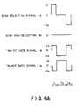
- Figure 4A shows a scanning selection signal S S , a scanning non-selection signal S N , a white data signal I W and a black data signal I B .
- Figure 4B shows a voltage waveform (I W - S S ) applied to a selected pixel (receiving a white data signal I W ) among the pixels (intersections between scanning electrodes and data electrodes) on a selected scanning electrode receiving a scanning selection signal S S , a voltage waveform (I B - S S ) applied to a non-selected pixel (receiving a black data signal I B ) on the same selected scanning electrode, and voltage waveforms applied to two types of pixels on non-selected scanning electrodes receiving a scanning non-selection signal S N .
- a nonselected pixel on a selected scanning electrode is supplied with a voltage -(V 1 +V 3 ) exceeding one threshold voltage of the ferroelectric liquid crystal to have the ferroelectric liquid crystal assume one orientation state providing a dark state, thus being written in "black".
- a selected pixel on the selected scanning electrode is supplied with a voltage (-V 1 +V 3 ) not exceeding the threshold voltages of the ferroelectric liquid crystal so that the orientation state of the ferroelectric liquid crystal is not changed.
- a phase t 2 the selected pixel on the selected scanning electrode is supplied with a voltage (V 2 + 3 ) exceeding the other threshold voltage of the ferroelectric liquid crystal to have the ferroelectric liquid crystal assume the other orientation state providing a bright state thus being written in "white". Further, in the phase t 2 , the nonselected pixel on the selected pixel is supplied with a voltage (V 2 -V 3 ) below the threshold voltages of the ferroelectric liquid crystal to retain the orientation state which is provided in the previous phase t 1 . On the other hand, in phases t 1 and t 2 , the pixels on nonselected scanning electrodes are supplied with voltages ⁇ V 3 below the threshold voltages of the ferroelectric liquid crystal.
- the pixels on the selected scanning electrode are written in "white” or “black” in a writing phase T 1 including the phases t 1 and t 2 , and the pixels retain their written states even when they subsequently receive a scanning non-selection signal.
- phase T 2 of this embodiment voltages having polarities opposite to those of the data signals in the writing phase T 1 are applied through the data electrodes.
- the pixels on the non-selected scanning electrodes are supplied with an AC voltage so that the threshold characteristic of the ferroelectric liquid crystal is improved.
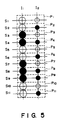
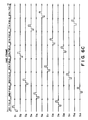
- Figure 4C is a time chart of a set of voltage waveforms providing a display state shown in Figure 5.
- a scanning selection signal is applied to the scanning electrodes with skipping of 5 lines apart in a field (one vertical scanning) and the scanning selection signal is applied to scanning electrodes which are not adjacent to each other in consecutive 6 fields.
- the scanning electrodes are selected 5 lines (electrodes) apart so that one frame scanning (one picture scanning) is effected in 6 fields of scanning (6 times of one vertical scanning).
- FIG 4D shows another embodiment using drive waveforms shown in Figure 4A.
- the scanning electrodes are selected two lines apart so that not-adjacent scanning electrodes are selected in consecutive three fields of scanning.
- Figures 6A and 6B show another driving embodiment used in the present invention.
- "black” is written in phase t 1 and "white” is written in phase t 2 .
- an auxiliary signal is applied through data electrodes so as to apply an AC voltage to the pixels at the time of non-selection similarly as in the previous embodiment.
- Such an auxiliary signal shows the effect as disclosed in US-A-4,655,561, etc.
- Figure 6C is a time chart showing application of scanning selection signals using driving waveforms shown in Figures 6A and 6B.
- the scanning selection signal is applied to the scanning electrodes with skipping of 7 lines apart and one frame scanning is completed in 8 fields of scanning. Also in this embodiment, the scanning selection signal is applied to not-adjacent scanning electrodes in consecutive 8 fields of scanning.
- a scanning selection signal may be applied to the scanning electrodes with skipping of 4 or more lines apart, preferably 5 - 20 lines apart.
- the peak values of the voltage signals V 1 , -V 2 and ⁇ V 3 may preferably be set to satisfy the relation of
- the pulse durations of these voltage signals may be set to 1 ⁇ sec - 1 msec, preferably 10 ⁇ sec - 100 ⁇ sec, and it is preferred to set a longer pulse duration at a lower temperature than at a higher temperature.
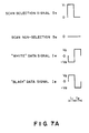
- Figures 7A and 7B show a set of driving waveforms in another embodiment. More specifically, Figure 7A shows a scanning selection signal S S , a scanning non-selection signal S N , a white data signal I W and a black data signal I B .
- Figure 4B shows a voltage waveform (I W - S S ) applied to a selected pixel (receiving a white data signal I W ) among the pixels (intersections between scanning electrodes and data electrodes) on a selected scanning electrode receiving a scanning selection signal S S , a voltage waveform (I B - S S ) applied to a non-selected signal (receiving a black data signal I B ) on the same selected scanning electrode, and voltage waveforms applied to two types of pixels on non-selected scanning electrodes receiving a scanning non-selection signal S N .
- the scanning electrodes prior to application of the above-mentioned scanning selection signal S S , are supplied with a clearing voltage signal V H which has a polarity opposite to that of the scanning selection signal S S (with respect to the voltage level of a non-selected scanning electrode) and has a voltage exceeding one threshold voltage of a ferroelectric liquid crystal, whereby the related pixels are oriented in advance to one orientation state of the ferroelectric liquid crystal to form a dark state, thus effecting a step of clearing into a "black” state.
- a selected pixel on a selected scanning electrode is supplied with a voltage -(V 1 + V 2 ) exceeding the other threshold voltage of the ferroelectric liquid crystal to result in a bright state based on the other orientation state of the ferroelectric liquid crystal, thus being written in "white".
- a non-selected pixel on the selected scanning electrode is supplied with a voltage (-V 1 + V 2 ) below the threshold voltages of the ferroelectric liquid crystal so that the orientation state of the ferroelectric liquid crystal is not changed thereby.
- the pixels on the non-selected scanning electrodes are supplied with voltages ⁇ V 2 which are below the threshold voltages of the ferroelectric liquid crystal in the phase t 1 .
- the pixels on the selected scanning electrode are written in either "white” or “black”, and the resultant states are retained even under subsequent application of scanning non-selection signals.
- phase t 2 of this embodiment voltages of polarities opposite to those of the data signals in phase t 1 are applied through the data electrodes.
- the pixels at the time of non-selection are supplied with an AC voltage so that the threshold characteristic of the ferroelectric liquid crystal can be improved.
- Figure 7C is a time for providing a display state shown in Figure 5 by using the driving waveforms shown in Figures 7A and 7B.
- a clearing voltage V H is applied to the scanning electrodes, and then the scanning selection signal is applied to the scanning electrodes (with skipping of) 5 lines apart so that the scanning selection is applied to scanning electrodes which are not adjacent to each other in consecutive 6 fields.
- the scanning electrodes are selected 5 lines apart so that one frame scanning (one picture scanning) is effected in 6 fields of scanning.
- FIG 7D shows another embodiment using the drive waveforms shown in Figures 7A and 7B.
- the scanning electrodes are selected two lines apart so that not-adjacent scanning electrodes are selected in consecutive three fields of scanning.
- Figure 7E shows another embodiment using the drive waveforms shown in Figures 7A and 7B, wherein only scanning signals are shown along with corresponding states of terminals Q 1 and Q 2 shown in Figure 8.
- one block is designated for 5 scanning electrodes each, and for each block, a clearing step is performed by application of a clearing voltage signal V H and then a scanning selection signal is sequentially applied to not-adjacent scanning electrodes.
- FIG 8 is a partial circuit diagram showing an output stage of a scanning electrode drive circuit for performing the drive of the above embodiment.
- the output stage includes terminals R 1 - R 5 , buffers 81 (B 1 - B 10 ...) connected to output lines S 1 - S 10 , and terminals Q 1 and Q 2 connected to the buffers 81 through selection lines 82.
- the output level of a buffer 81 is controlled by a selection line 82.
- buffers B 1 - B 5 are simultaneously turned on so as to transfer the levels of terminals R 1 - R 5 as they are to output lines S 1 - S 5 .
- the output lines S 1 - S 5 are all brought to a prescribed constant level so as to make the cells nonselective.
- a terminal Q 1 has the same function with respect to the buffers B 6 - B 10 .
- FIG. 9 is a block diagram of a circuit for use in another embodiment of the present invention.
- data signals are supplied to a display panel 90 through a common data electrode drive circuit 91.
- a scanning electrode drive circuit 92 is divided into three sections #1, #2 and #3 so as to control display areas A, B and C, respectively, of the display panel 90.
- the scanning electrode drive circuits #1 - #3 are separately composed of their own logic circuits, and scanning electrodes for writing are first selected by input signals Q 1 - Q 3 and used to write in the areas A, B and C separately, so that writing of a large capacity and high density can be performed at a high speed.
- FIGS 10A and 10B show a set of driving waveforms used in another embodiment of the present invention. Similarly as in the previous embodiment, prior to application of a scanning selection signal, a clearing voltage V H is applied, so that the whole picture area or a block thereof is cleared into "black” (or "white”).
- Figure 10C is a time chart showing a time relation of applying scanning selection signals using the driving waveforms shown in Figures 10A and 10B, wherein only scanning selection signals are shown.
- a scanning selection signal is applied to the scanning electrodes with skipping of 6 lines apart so that one frame scanning is completed in 7 fields of scanning. Also in this embodiment, the scanning selection signal is applied to scanning electrodes which are not adjacent to each other in consecutive 7 fields of scanning.
- a scanning selection signal may be applied to 4 or more lines apart, preferably 5 - 20 lines apart.
- Figure 10D shows another embodiment using the driving waveforms shown in Figures 10A and 10B, wherein only scanning signals are shown.
- one block is designated for each 5 scanning electrodes, and for each block, a clearing step is performed by applying a clearing voltage signal V H , followed by sequential application of a scanning selection signal to scanning electrodes which are not adjacent to each other.
- one picture scanning is performed by sequentially effecting block scanning operations for blocks which are not adjacent to each other.
- the peak values of the voltage signals V H , V 1 and ⁇ V 2 in Figures 7A - 7E may preferably be set to satisfy the relations of:
- the peak values of the voltage signals V H , V 1 , -V 2 and ⁇ V 3 may preferably be set to satisfy the relations of:
- the pulse durations of these voltage signals in Figures 7 and 10 may be set to 1 ⁇ sec - 1 msec, preferably 10 ⁇ sec - 100 ⁇ sec and it is preferred to set a longer pulse duration at a lower temperature than at a high temperature.
- Figure 11A shows a scanning selection signal S S , a scanning non-selection signal S N , a white data signal I W and a black data signal I B in another embodiment of the present invention.
- Figure 11B shows a voltage waveform (I W - S S ) applied to a selected pixel (receiving a white data signal I W ) among the pixels (intersections between scanning electrodes and data electrodes) on a selected scanning electrode receiving a scanning selection signal S S , a voltage waveform (I B - S S ) applied to a non-selected signal (receiving a black data signal I B ) on the same selected scanning electrode, and voltage waveforms applied to two types of pixels on non-selected scanning electrodes receiving a scanning non-selection signal S N .
- a phase T 1 is used for causing one orientation state of a ferroelectric liquid crystal regardless of the types of data pulses.
- cross nicol polarizers are set so as to provide a black display based on a dark state when the ferroelectric liquid crystal assumes one orientation state, but it is also possible to set the polarizers so as to provide a bright state corresponding to one orientation state.
- a former (sub-)phase t 1 in the phase T 1 is used as a phase for applying a part of a data signal applied in association with a previous scanning selection signal.
- phase t 3 a selected pixel on a selected scanning electrode receiving a scanning selection signal S S is supplied with a voltage -(V 1 +V 3 ) to result in the other orientation state of the ferroelectric liquid crystal, whereby a white display based on a bright state is given after clearing into a "black" display in the phase T 1 .
- another pixel (non-selected pixel) on the selected scanning electrode is supplied with a voltage -(V 1 -V 3 ) which however is set to a voltage not changing the orientation state of the ferroelectric liquid crystal, so that the black display state resultant in the phase T 1 is retained in the phase t 3 .
- the pixels on the non-selected scanning electrodes receiving a scanning non-selection signal are supplied with voltages ⁇ V 3 not changing the orientation states of the ferroelectric liquid crystal.
- the written states are retained as they are during one field or frame scanning period.
- phase t 2 of this embodiment voltages having polarities opposite to those of the data pulses in the writing phase t 3 are applied through the data electrodes.
- the pixels on the non-selected scanning electrodes are supplied with an AC voltage, so that the threshold characteristic of the ferroelectric liquid crystal is improved.
- Figure 11C is a time chart of a set of voltage waveforms providing a display state as shown in Figure 5 with respect to scanning electrodes S 1 - S 8 .
- a scanning selection signal is applied to the scanning electrodes with skipping of 3 lines apart in a field and the scanning selection signal is applied to scanning electrodes which are not adjacent to each other in consecutive 4 fields.
- the scanning electrodes are selected 3 lines apart, so that one frame scanning (one picture scanning) is performed in 4 fields of scanning.
- FIG 11D shows another embodiment using drive waveforms shown in Figure 11A.
- the scanning electrodes are selected 5 lines apart so that not-adjacent scanning electrodes are selected in consecutive 6 fields of scanning.
- the scanning pulses and data pulses are set to satisfy the relationships of
- 3
- These relationships are not necessarily essential, but for example, a relationship of
- a
- Figures 12A and 12B show a set of driving waveforms used in another driving embodiment.
- all or a prescribed number of the pixels on a selected scanning electrode are cleared into "black" in phase T 1 regardless of the types of data signals concerned, and in writing phase t 3 , a selected pixel among the pixels is supplied with a voltage providing a white display and the other pixels among the pixels are supplied with a voltage maintaining the black display.
- Phase t 4 is a phase for applying auxiliary signals through the data electrodes so as to always apply an AC voltage to the pixels at the time of non-selection, and these auxiliary signals correspond to a part of data signals for previous data entry applied in phase t 1 .
- the effect of application of such an auxiliary signal has been classified, e.g., in US-A-4,655,561.
- Figure 12C is a time chart of a set of voltage waveforms using those shown in Figures 12A and 12B for providing a display state as shown in Figure 5, with respect to scanning electrodes S 1 - S 8 .
- a scanning selection signal is applied to the scanning electrodes with skipping of 3 lines apart and one frame scanning is completed by 4 fields of scanning.
- the scanning selection signal is applied to scanning electrodes which are not adjacent to each other in four scanning fields.
- a former pulse (voltage: -V 2 ) of a subsequent scanning selection signal is applied immediately after application of a latter pulse (voltage: V 1 ) of a preceding scanning selection signal.
- Phase T 1 is a clearing phase similar to the one in the previous embodiment and phase t 3 is a writing phase similar to the one in the previous embodiment.
- Phases t 2 and t 4 correspond to phases for applying auxiliary signals used in the previous embodiment so as to always apply AC voltages to pixels at the time of non-selection, whereby the threshold characteristic of the ferroelectric liquid crystal is improved.
- phase t 1 is also used for applying a part of a data signal associated with a previous scanning selection signal.
- Figure 13C is a time chart of a set of voltage waveforms using those shown in Figures 13A and 13B for providing a display state as shown in Figure 5, with respect to scanning electrodes S 1 - S 12 .
- a scanning selection signal is applied to the scanning electrodes with skipping of 5 lines apart and one frame scanning is completed by 6 fields of scanning.
- the scanning selection signal is applied to scanning electrodes which are not adjacent to each other in 6 scanning fields.
- a former pulse (voltage: -V 2 ) of a subsequent scanning selection signal is applied immediately after application of a latter pulse (voltage: V 1 ) of a preceding scanning selection signal.
- a former pulse of a subsequent scanning selection signal is applied simultaneously with or immediately after the application of a latter pulse of a previous scanning selection signal, and also the subsequent scanning selection signal is applied before the completion of a data signal applied for data entry associated with the previous scanning selection signal.
- a scanning selection signal may be applied to the scanning electrodes with skipping of 4 or more lines apart, preferably 5 - 20 lines apart.
- the peak values of the voltage signals V 1 , -V 2 and ⁇ V 3 may preferably be set to satisfy the relation of
- the pulse durations of these voltage signals may be set to 1 ⁇ sec - 1 msec, preferably 10 ⁇ sec - 100 ⁇ sec, and it is preferred to set a longer pulse duration at a lower temperature than at a higher temperature.
- Figure 14 is a circuit diagram showing a liquid crystal display drive control system used in the present invention.
- the memories M 1 , M 2 and M 3 are supplied with data through a data bus DB and are controlled through a control bus CB with respect to writing/readout and addressing.
- the system further includes a decoder DC to which a field switching signal FC is supplied, a multiplier MPX for selecting one of the outputs from the memories M1, M2 and M3, a monostable multi-Vibrator MM supplying a gate signal GT to an AND gate to which clock signals CK are also supplied from a clock pulse oscillator FG, a counter CNT to which now-scanning clock signals F are supplied from the AND gate, a serial input/parallel output shift register SR, a column drive circuits DR 1 - DR 4 and row drive circuits DR 5 - DR 8 .
- Figure 15 shows gradation data for respective pixels for one gradational picture scanning (referred to as "one frame").
- the highest level bit HSB, the medium level but MSB and the lowest level bit LSB of each gradation data are inputted to the memories M3, M2 and M1, respectively, through the data but DB.
- one picture scanning (referred to as "one sub-frame") switching signal FC is generated at time t 1
- the decoder DC sets the multiplexer MPX to receive data from the memory M1.
- the signal FC is inputted to the monostable multi-Vibrator MM to generate a gate signal GT and open the AND gate, thereby to supply four clock signals CK as a row scanning signal F to the counter CNT.
- the counter CNT turns the driver DR5 on receiving the first clock signal.
- the shift register SR is loaded with the first row data of the memory M1, and only the driver DR3 is made on.
- a liquid crystal pixel A 13 alone is set to a dark level and the other liquid crystal pixels A 11 , A 12 and A 14 are set to a bright level.
- the row scanning signal F is inputted to a controller (not shown) as a memory row scanning signal
- the memory M1 supplies subsequent second row data to the shift register
- the driver DR6 is turned on receiving a subsequent row scanning signal F
- the second row data of the memory M1 are respectively supplied to the drivers DR1 - DR4 from the shift register SR.
- the drivers DR2, DR3 and DR4 are turned on to set the pixels A 22 , A 23 and A 24 to the dark level and the pixel A 21 to the bright level.
- the above operations are repeated for the third and fourth rows.
- the counter CNT supplies a memory switching demand signal MC to a controller (not shown) to select the memory M2 to start a second sub-frame.
- the respective liquid crystal pixels set to bright or dark states retain their states because the ferroelectric liquid crystal has a memory function.
- the multiplexer MPX selects data from the memory M2 based on a sub-frame switching signal FC, and a row scanning signal F is supplied to the counter CNT and the shift register SR based on a gate signal GT. Then, row scanning is performed in a similar cycle as in the first sub-frame to set the respective liquid crystal pixels to dark or bright states.
- a third frame is performed in a similar manner.
- the periods of the first, second and third sub-frames are set to ratios of 1:2:4 in the same values as the weights of the respective bits.
- the gradation data for, e.g., the pixel A 12 is 2 as shown in Figure 16D, so that the pixel A 12 is set to the dark level only in the second sub-frame period and assumers the dark state for 2/7 of one frame period.
- the gradation data for the pixel A 24 is 5, so that the pixel A 24 is set to the dark level for the first and third sub-frame periods and assumes the dark state for 5/7 of one frame period.
- the gradation data for the pixel A 42 is 7, so that the pixel A 42 is caused to assume the dark state for all the sub-frame periods.
- gradational display at 8 levels can be performed in this embodiment.
- an apparent intermediate toner or gray scale can be displayed by controlling the proportion of a display time in one frame period, i.e., a display duty.
- an intermediate gradational display can be generally performed if one frame is divided into a plurality, i.e., two or more, of sub-frames.
- the sub-frame periods are set to have different durations corresponding to the weights of data bits in the above embodiments, but the sub-frames can also be provided with equal durations by equal division. In this case, however, it is necessary to decode gradation data.
- Figure 18 shows examples of drive waveforms applied to a scanning electrode S 1 and data electrodes I 1 and I 2 in one frame and first to third sub-frames contained therein.
- the first, second and third sub-frames are set to have duration ratios of 1:2:4, respectively.
- the intersection of the scanning electrode S 1 and data electrode I 1 is provided with a gradational display corresponding to a weighted total of BR (bright) in the first sub-frame, BR in the second sub-frame and D (dark) in the third sub-frame.
- intersection of the scanning electrode S 1 and data electrode I 2 is provided with a gradational display corresponding to a weighted total of BR in the first sub-frame, D in the second sub-frame and D in the third sub-frame. Further, in this embodiment, the intersection of the scanning electrode S 1 and data electrode I 2 is set to have an area which is two times that of the intersection of the scanning electrode S 1 and data electrode I 1 , and an increased variety of gradational display is performed based on such intersectional area ratios.
- various ferroelectric liquid crystal devices can be used, including an SSFLC device as disclosed by Clark et al in US-A-4,367,924, a ferroelectric liquid crystal device in an alignment state retaining a helical residue as disclosed by Isogai et al in US-A-4,586,791 and a ferroelectric liquid crystal device in an alignment state as disclosed in U.K. Patent GB-A-2159635.
- FIG. 19 is a block diagram illustrating a structural arrangement of an embodiment of the display apparatus according to the present invention.
- a display panel 1901 is composed of scanning electrodes 1902, data electrodes 1903 and a ferroelectric liquid crystal disposed therebetween. The orientation of the ferroelectric liquid crystal is controlled by an electric field at each intersection of the scanning electrodes 1902 and data electrodes 1903 formed due to voltages applied across the electrodes.
- the display apparatus includes a data electrode driver circuit 1904, which in turn comprises an image data shift register 19041 for storing image data serially supplied from a data signal line 1906, a line memory 19042 for storing image data supplied in parallel from the image data shift register 19041, a data electrode driver 19043 for supplying voltages to data electrodes 1903 according to the image data stored in the line memory 19042, and a data side power supply changeover unit 19044 for changing over among voltages V D , 0 and -V D supplied to the data electrodes 1903 based on a signal from a changeover control line 1911.
- a data electrode driver circuit 1904 which in turn comprises an image data shift register 19041 for storing image data serially supplied from a data signal line 1906, a line memory 19042 for storing image data supplied in parallel from the image data shift register 19041, a data electrode driver 19043 for supplying voltages to data electrodes 1903 according to the image data stored in the line memory 19042, and a data side power
- the display apparatus further includes a scanning electrode driver circuit 1905, which in turn comprises a decoder 19051 for designating a scanning electrode among all the scanning electrodes based on a signal received from a scanning address data line 1907, a scanning electrode driver 19052 for applying voltages to the scanning electrodes 1902 based on a signal from the decoder 19051, and a scanning side power supply changeover unit 19053 for changing over among voltages V S , 0 and -V S supplied to the scanning electrodes 1902 based on a signal from a changeover control line 1911.
- a scanning electrode driver circuit 1905 which in turn comprises a decoder 19051 for designating a scanning electrode among all the scanning electrodes based on a signal received from a scanning address data line 1907, a scanning electrode driver 19052 for applying voltages to the scanning electrodes 1902 based on a signal from the decoder 19051, and a scanning side power supply changeover unit 19053 for changing over among voltages V S , 0
- the display apparatus further includes a CPU 19019, which receives clock pulses from an oscillator 1909, controls the image memory 1910, and controls the signal transfer over the data signal line 1906, scanning address data line 1907 and changeover control line 1911.
- a CPU 19019 which receives clock pulses from an oscillator 1909, controls the image memory 1910, and controls the signal transfer over the data signal line 1906, scanning address data line 1907 and changeover control line 1911.
- the present invention it is possible to effectively suppress the occurrence of flicker caused by scanning drive at a low frame frequency as low as 2 - 15 Hz. Particularly, the occurrence of flicker is prevented for a long scanning selection period set at a low temperature, whereby it is possible to provide a high-quality display picture over a substantially wide temperature range. According to the present invention, it is further possible to effectively prevent a phenomenon of image flow, whereby a high-quality display picture, particularly gradational display picture, can be formed also in this respect.
Landscapes
- Engineering & Computer Science (AREA)
- Chemical & Material Sciences (AREA)
- Crystallography & Structural Chemistry (AREA)
- Physics & Mathematics (AREA)
- Computer Hardware Design (AREA)
- General Physics & Mathematics (AREA)
- Theoretical Computer Science (AREA)
- Liquid Crystal Display Device Control (AREA)
- Liquid Crystal (AREA)
Abstract
Description
- The present invention relates to a display apparatus using a ferroelectric liquid crystal, particularly a liquid crystal apparatus free from occurrence of noticeable flicker.
- In a liquid crystal television panel using the conventional active-matrix drive system, thin film transistors (TFT) are disposed in a matrix corresponding to respective pixels, and a gradational display is performed in such a manner that a TFT is supplied with a gate-on pulse to make the source and drain conductive between each other, an image signal is supplied through the source at that time to be stored in a capacitor, and a liquid crystal (e.g., a twisted nematic (TN) liquid crystal) at the pixel is driven corresponding to the stored signal while modulating the voltage of the image signal.
- In such a television panel of the active matrix drive system using a TN-liquid crystal, each TFT used has a complicated structure requiring many steps for production, so that a high production cost is incurred and also it is difficult to form a thin film semiconductor of, e.g., polysilicon or amorphous silicon constituting TFTs over a wide area.
- On the other hand, a display panel of the passive matrix system using a TN-liquid crystal has been known as one which can be attained at a low production cost. In this type of display panel, however, a duty ratio, i.e., a ratio of time wherein a selected point is supplied with an effective electric field during scanning of one picture (one frame), is decreased at a rate of 1/N if the number (N) of scanning lines is increased so that crosstalk is caused and an image of high contrast cannot be formed. Further, as the duty ratio is lowered, it becomes difficult to control the gradation of each pixel by voltage modulation. Thus, this type of liquid crystal panel is not suitable as a display panel with a high density of lines, particularly as a liquid crystal television panel.
- In recent years, the use of a liquid crystal device showing bistability has been proposed by Clark and Lagerwall as an improvement to the conventional liquid crystal devices in US-A-4,367,924; JP-A-56107216; etc. As the bistable liquid crystal, a ferroelectric liquid crystal (hereinafter sometimes abbreviated as "FLC") showing chiral smectic C phase (SmC*) or H phase (SmH*) is generally used. The ferroelectric liquid crystal assumes either a first optically stable state or a second optically stable state in response to an electric field applied thereto and retains the resultant state in the absence of an electric field, thus showing a bistability. Further, the ferroelectric liquid crystal quickly responds to a change in electric field, and thus the ferroelectric liquid crystal device is expected to be widely used in the field of a high-speed and memory-type display apparatus, etc.
- However, the above-mentioned ferroelectric liquid crystal device has involved a problem of flickering at the time of multiplex driving. For example, European Laid-Open Patent Application (EP-A) 149899 discloses a multiplex driving method wherein a scanning selection signal of an AC voltage the polarity of which is reversed (or the signal phase of which is reversed) is applied for each frame to selectively write a "white" state (in combination with cross nicol polarizers arranged to provide a "bright" state at this time) in a former frame and then selectively write a "black" state (in combination with the cross nicol polarizers arranged to provide a "dark" state at this time) in a subsequent frame. In addition to the above driving method, those driving methods as disclosed by US-A-4548476 and US-A-4655561 have been known.
- In such a driving method, at the time of selective writing of "black" after a selective writing of "white", a pixel selectively written in "white" in the previous frame is placed in a half-selection state, whereby the pixel is supplied with a voltage which is smaller than the writing voltage but is still effective. As a result, at the time of selective writing of "black" in the multiplex driving method, selected pixels for writing "white" constituting the background of a black image are wholly supplied with a half-selection voltage in a 1/2 frame cycle (1/2 of a reciprocal of one frame or picture scanning period) so that the optical characteristic of the white selection pixels varies in each of the 1/2 frame cycle. As a number of white selection pixels is much larger than the number of black selection pixels in a display of a black image, e.g., character, on a white background, the white background causes flickering. Occurrence of a similar flickering is observable also on a display of white characters on the black background opposite to the above case. In case where an ordinary frame frequency is 30 Hz, the above half-selection voltage is applied at a frequency of 15 Hz which is a 1/2 frame frequency, so that it is sensed by an observer as a flickering to remarkably degrade the display quality.
- Particularly, in driving of a ferroelectric liquid crystal at a low temperature, it is necessary to use a longer driving pulse (scanning selection period) than that used at a 1/2 frame frequency of 15 Hz for a higher temperature to necessitate scanning drive at a lower 1/2 frame frequency of, e.g., 5 - 10 Hz. This leads to occurrence of a noticeable flickering due to a low frame frequency drive at a low temperature.
- Document FR-A-2 578 670 discloses an optical modulation device and its corresponding driving method. In detail, an active matrix display system is described including scanning electrodes and data electrodes, a ferroelectric liquid crystal showing a first and a second orientation state, as well as driving means for applying prescribed voltages to only selected picture elements. Thus, the circuit is simplified and its structure is improved so that cross-talk cannot occur. However, neither the occurrence of a display flickering caused by a low frame frequency nor its suppression by using a time sharing method is disclosed in this document.
- Document EP-A-0 261 901 relates to a display device and especially to a grey-scale television display. In order to define one out of a plurality of grey levels or to produce half tones, each line in the picture is addressed, e.g. four times, during a picture period, at respective intervals of line periods and each pixel element can be turned on for any one or more of these intervals as considered appropriate. Thus, a display data portion, of e.g. four bits, defines one of sixteen grey levels and may prevent significant errors in half tone levels. That is, by using time division and divided-pixel systems simultaneously, the number of available half tone levels is not limited by the space available for conducting lines or the speed of switching the liquid crystal. However, this document does not disclose a liquid crystal apparatus using interlaced scan drive of the ferroelectric liquid crystal and, thus, is not capable of realizing a gradational display free from flickering.
- Finally, document EP-A-0 306 011, which falls within the terms of art. 54 (3) EPC, discloses a method for a driving display device utilizing a ferroelectric crystal which accomplishes, according to a time sharing method, a display of plural gradations. In detail, the disclosed liquid crystal apparatus comprises an electrode-matrix composed of scanning electrodes and data electrodes, a ferroelectric liquid crystal and driving means. The special driving method of this conventional driving means accomplishes a display in multiple gradations in a reduced time. However, also this document does not disclose a liquid crystal apparatus which prevents the occurrence of flickering caused by a low frame frequency scanning.
- In contrast to this prior art, it is an object of the present invention to provide a liquid crystal apparatus, wherein occurrence of flickering caused by a low frame frequency scanning drive is suppressed.
- According to a first aspect of the present invention this object is achieved by a liquid crystal apparatus, comprising a liquid crystal device comprising an electrode matrix composed of scanning electrodes and data electrodes disposed to intersect said scanning electrodes, and a ferroelectric liquid crystal showing a first and a second orientation state disposed between said scanning electrodes and said data electrodes; and a driving means for effecting one picture scanning in plural times of vertical scanning including a first drive means for applying scanning signals to said scanning electrodes and a second drive means for applying data signals to said data electrodes, said liquid crystal apparatus being characterized in that said scanning signals include a scanning selection signal which is applied to scanning electrodes two or more scanning electrodes apart in one vertical scanning, and which is applied to scanning electrodes which are not adjacent to each other in at least two consecutive times of vertical scanning, said scanning selection signal having an alternating voltage of one polarity and of the other polarity with respect to the voltage level of a nonselected scanning electrode, and said data signals include a data signal which is applied to a selected data electrode and which provides a voltage causing the first orientation state of said ferroelectric liquid crystal in combination with the voltage of one polarity of the scanning selection signal, and a data signal which is applied to another data electrode, siad data signal providing a voltage causing the second orientation state of the ferroelectric liquid crystal in combination with the voltage of the other polarity of the scanning selection signal.
- According to a second aspect of the present invention this object is achieved by a liquid crystal apparatus, comprising a liquid crystal device comprising an electrode matrix composed of scanning electrodes and data electrodes disposed to intersect said scanning electrodes, and a ferroelectric liquid crystal showing a first and a second orientation state disposed between said scanning electrodes and said data electrodes; and a driving means for effecting one picture scanning in plural times of vertical scanning including a first drive means for applying scanning signals to said scanning electrodes and a second drive means for applying data signals to said data electrodes, said liquid crystal apparatus being characterized in that said first drive means applies, prior to application of a scanning selection signal, a clearing voltage causing the first orientation state of the ferroelectric liquid crystal to the intersections of the plural scanning electrodes and data electrodes by applying a clearing pulse having a voltage of one polarity to said plural scanning electrodes and a voltage to said data electrodes, said first drive means applies, after the application of said clearing pulse to said plural scanning electrodes, the scanning selection signal to scanning electrodes two or more scanning electrodes apart in one vertical scanning, and to scanning electrodes which are not adjacent to each other in at least two consecutive times of vertical scanning, said scanning selection signal having a voltage of a polarity opposite to that of said voltage of one polarity with respect to the voltage level of a non-selected scanning electrode; and said second driving means applies to a selected data electrode a voltage signal which provides a voltage causing the second orientation state of the ferroelectric liquid crystal in combination with the scanning selection signal.
- According to a third aspect of the present invention this object is achieved by a liquid crystal apparatus, comprising a liquid crystal device comprising an electrode matrix composed of scanning electrodes and data electrodes disposed to intersect said scanning electrodes, and a ferroelectric liquid crystal showing a first and a second orientation state disposed between said scanning electrodes and said data electrodes; and a driving means for effecting one picture scanning in plural times of vertical scanning including a first drive means for applying scanning signals to said scanning electrodes and a second drive means for applying data signals to said data electrodes, said liquid crystal apparatus being characterized in that said first drive means sequentially applies a scanning selection signal to scanning electrodes two or more scanning electrodes apart between successively selected scanning electrodes, wherein said scanning selection signal is applied to scanning electrodes which are not adjacent to each other in at least two consecutive times of vertical scanning, said scanning selection signal having a former voltage of one polarity and a latter voltage of an opposite polarity with respect to the voltage level of a nonselected scanning electrode, two successive scanning selection signals including a former and a latter scanning selection signal being applied to the scanning electrodes in such a time relationship that said former voltage of one polarity of the latter scanning selection signal is commenced to be applied before the completion of a data signal associated with the former scanning selection signal and after the application of the voltage of one polarity of the former scanning selection signal, and said second drive means applies to all or a prescribed number of said data electrodes a voltage signal which provides a clearing voltage causing the first orientation state of said ferroelectric liquid crystal in combination with said voltage of one polarity of said scanning selection signal, and applying to a selected data electrode a voltage signal which provides a voltage causing the second orientation state of said ferroelectric liquid crystal.
- These and other objects, features and advantages of the present invention will become more apparent upon a consideration of the following description of the preferred embodiments of the present invention taken in conjunction with the accompanying drawings.
-
- Figure 1 is a plan view of an electrode matrix or matrix electrode structure of an FLC device used in the present invention; Figure 2 is a sectional view taken along the line A-A' of the FLC device shown in Figure 1;
- Figure 3 is an illustration of intermediate gradations;
- Figures 4A - 4D are driving waveform diagrams used in the invention;
- Figure 5 is a schematic illustration of a display state of a matrix electrode structure;
- Figures 6A - 6C show a set of driving waveform diagrams used in the invention;
- Figures 7A and 7B show another set of driving waveform diagrams used in the invention;
- Figure 8 is a block diagram of output means of a scanning electrode drive circuit used in the present invention;
- Figure 9 is a block diagram illustrating an embodiment of the present invention;
- Figures 10A - 10D, Figures 11A - 11D, Figures 12A - 12C and Figures 13A - 13C, respectively, show another set of driving waveform diagrams used in the invention;
- Figure 14 is a circuit diagram illustrating a drive control circuit used in the invention;
- Figures 15 and 16A - 16D are illustrative gradation data at pixels;
- Figure 17 is a time chart used in a drive system according to the invention;
- Figure 18 is another example of driving waveform used in the invention; and
- Figure 19 is a block diagram of a liquid crystal apparatus according to the invention.
- The present invention will be explained based on an embodiment applicable to a ferroelectric liquid crystal (FLC).
- Figure 1 is a schematic plan view of a matrix electrode structure of an FLC device according to an embodiment of the present invention and Figure 2 is a sectional view taken along the line A-A′ in Figure 1. Referring to these figures, the FLC device comprises upper electrodes 11A (A1, A2, A3, ...) and 11B (B1, B2, B3, B4, ...) constituting data electrodes, and
lower electrodes 12 constituting scanning electrodes C (C0, C1, C2, C3, ...). These data electrodes 11A, 11B and scanningelectrodes 12 are formed onglass substrates FLC material 15 disposed therebetween. As shown in the figures, one pixel is constituted by a region E surrounded by a dashed line, i.e., a region where a scanning electrode C (C2 is shown as an example) and two data electrodes A (A2) and B (B2) (electrode width: A > B). In this instance, each data electrode A is composed to have a wider electrode width then an accompanying data electrode B. The scanning electrodes C and the data electrodes A, B are respectively connected to a power supply (not shown) through switches SW (or equivalents thereof). The switches SW are also connected to a controller unit (not shown) for controlling the ON/OFF of the switches. Based on this arrangement, a gray scale display in the pixel E, for example, composed of the scanning electrode C2 and the data electrodes A and B, may be effected under the control by means of the controller circuit as follows. When the scanning electrode C2 is selected or scanned, a white display state ("W") is given by applying a "W" signal to the data electrodes A2 and B2 respectively; a display state of "Gray 1" is given by applying a "W" signal to A2 and a black ("B") signal to B2; a display state of "Gray 2" is given by applying a "B" signal to A2 and a "W" signal to B2; and a black display state ("B") is given by applying a "B" signal to A2 and B2 respectively. Figure 3 shows the resultant states W,Gray 1,Gray 2 and B constituting a gray scale. - In this way, a gray scale of 4 levels can be realized by using FLC which per se is essentially capable of only a binary expression.
- In a preferred embodiment of the present invention, a pixel E is composed of a plural number (n) of intersections of electrodes having intersection areas giving a geometric series of ratios such as 1:2:4:8: ...:2n-1 (the minimum intersection area is taken as 1 (unit)).
- In the present invention, if a scanning electrode is divided into two electrode stripes having widths C and D and combined with the data electrodes A and B (A ≠ B), 8 gradation levels can be provided when C = D and 16 gradation levels can be provided when C ≠ D.
- Further, in case where only the data electrode side is split into electrodes A and B, if their widths are set to be equal (A = B) and color filters in complementary colors are disposed on the electrodes A and B, a color display of four colors may be possible. For example, if a complementary color relationship of A = yellow and B = blue or A = magenta and B = green is satisfied, display of four colors of white, black, A's color and B's color becomes possible.
- Referring to Figure 2, the
polarizers - The electrode matrix shown in Figure 1 may be driven by a driving method as will be described hereinbelow, which however is also applicable to an electrode matrix comprising scanning electrodes and data electrodes with equal electrode widths.
- Figure 4A shows a scanning selection signal SS, a scanning non-selection signal SN, a white data signal IW and a black data signal IB. Figure 4B shows a voltage waveform (IW - SS) applied to a selected pixel (receiving a white data signal IW) among the pixels (intersections between scanning electrodes and data electrodes) on a selected scanning electrode receiving a scanning selection signal SS, a voltage waveform (IB - SS) applied to a non-selected pixel (receiving a black data signal IB) on the same selected scanning electrode, and voltage waveforms applied to two types of pixels on non-selected scanning electrodes receiving a scanning non-selection signal SN. According to Figures 4A and 4B, in a phase t1, a nonselected pixel on a selected scanning electrode is supplied with a voltage -(V1+V3) exceeding one threshold voltage of the ferroelectric liquid crystal to have the ferroelectric liquid crystal assume one orientation state providing a dark state, thus being written in "black". In this phase t1, a selected pixel on the selected scanning electrode is supplied with a voltage (-V1+V3) not exceeding the threshold voltages of the ferroelectric liquid crystal so that the orientation state of the ferroelectric liquid crystal is not changed. In a phase t2, the selected pixel on the selected scanning electrode is supplied with a voltage (V2+3) exceeding the other threshold voltage of the ferroelectric liquid crystal to have the ferroelectric liquid crystal assume the other orientation state providing a bright state thus being written in "white". Further, in the phase t2, the nonselected pixel on the selected pixel is supplied with a voltage (V2-V3) below the threshold voltages of the ferroelectric liquid crystal to retain the orientation state which is provided in the previous phase t1. On the other hand, in phases t1 and t2, the pixels on nonselected scanning electrodes are supplied with voltages ±V3 below the threshold voltages of the ferroelectric liquid crystal. As a result, in this embodiment, the pixels on the selected scanning electrode are written in "white" or "black" in a writing phase T1 including the phases t1 and t2, and the pixels retain their written states even when they subsequently receive a scanning non-selection signal.
- Further, in phase T2 of this embodiment, voltages having polarities opposite to those of the data signals in the writing phase T1 are applied through the data electrodes. As a result, as shown at the lower part of Figure 4B, the pixels on the non-selected scanning electrodes are supplied with an AC voltage so that the threshold characteristic of the ferroelectric liquid crystal is improved.
- Figure 4C is a time chart of a set of voltage waveforms providing a display state shown in Figure 5. In this embodiment, a scanning selection signal is applied to the scanning electrodes with skipping of 5 lines apart in a field (one vertical scanning) and the scanning selection signal is applied to scanning electrodes which are not adjacent to each other in consecutive 6 fields. In other words, in this embodiment, the scanning electrodes are selected 5 lines (electrodes) apart so that one frame scanning (one picture scanning) is effected in 6 fields of scanning (6 times of one vertical scanning). As a result, the occurrence of a flicker attributable to a low frame frequency drive can be remarkably suppressed even at a lower temperature requiring a longer scanning selection period (T1+T2) and accordingly under a scanning drive at a low frame frequency (of, e.g., 5 - 10 Hz). Further, as not-adjacent scanning electrodes are selected in consecutive 6 fields of scanning, image flow is effectively removed.
- Figure 4D shows another embodiment using drive waveforms shown in Figure 4A. In this embodiment, the scanning electrodes are selected two lines apart so that not-adjacent scanning electrodes are selected in consecutive three fields of scanning.
- Figures 6A and 6B show another driving embodiment used in the present invention. According to Figures 6A and 6B, "black" is written in phase t1 and "white" is written in phase t2. In an intermediate phase T2, an auxiliary signal is applied through data electrodes so as to apply an AC voltage to the pixels at the time of non-selection similarly as in the previous embodiment. Such an auxiliary signal shows the effect as disclosed in US-A-4,655,561, etc.
- Figure 6C is a time chart showing application of scanning selection signals using driving waveforms shown in Figures 6A and 6B. In the drive embodiment shown in Figure 6C, the scanning selection signal is applied to the scanning electrodes with skipping of 7 lines apart and one frame scanning is completed in 8 fields of scanning. Also in this embodiment, the scanning selection signal is applied to not-adjacent scanning electrodes in consecutive 8 fields of scanning.
- The present invention is not restricted to the above-described embodiments. Particularly, a scanning selection signal may be applied to the scanning electrodes with skipping of 4 or more lines apart, preferably 5 - 20 lines apart. Further, in the above embodiments, the peak values of the voltage signals V1, -V2 and ±V3 may preferably be set to satisfy the relation of |V1| = |-V2| > |±V3|, particularly |V1| = |-V2| ≧ 2|±V3|. Further, the pulse durations of these voltage signals may be set to 1 µsec - 1 msec, preferably 10 µsec - 100 µsec, and it is preferred to set a longer pulse duration at a lower temperature than at a higher temperature.
- Figures 7A and 7B show a set of driving waveforms in another embodiment. More specifically, Figure 7A shows a scanning selection signal SS, a scanning non-selection signal SN, a white data signal IW and a black data signal IB. Figure 4B shows a voltage waveform (IW - SS) applied to a selected pixel (receiving a white data signal IW) among the pixels (intersections between scanning electrodes and data electrodes) on a selected scanning electrode receiving a scanning selection signal SS, a voltage waveform (IB - SS) applied to a non-selected signal (receiving a black data signal IB) on the same selected scanning electrode, and voltage waveforms applied to two types of pixels on non-selected scanning electrodes receiving a scanning non-selection signal SN.
- In this embodiment, prior to application of the above-mentioned scanning selection signal SS, the scanning electrodes are supplied with a clearing voltage signal VH which has a polarity opposite to that of the scanning selection signal SS (with respect to the voltage level of a non-selected scanning electrode) and has a voltage exceeding one threshold voltage of a ferroelectric liquid crystal, whereby the related pixels are oriented in advance to one orientation state of the ferroelectric liquid crystal to form a dark state, thus effecting a step of clearing into a "black" state. In this instance, it is also possible to adopt a step of clearing into a "white" state based on a bright state. In this embodiment, however, the clearing step into black is adopted because of less occurrence of flicker.
- According to Figures 7A and 7B, in a phase t1, a selected pixel on a selected scanning electrode is supplied with a voltage -(V1 + V2) exceeding the other threshold voltage of the ferroelectric liquid crystal to result in a bright state based on the other orientation state of the ferroelectric liquid crystal, thus being written in "white". In this phase t1, a non-selected pixel on the selected scanning electrode is supplied with a voltage (-V1 + V2) below the threshold voltages of the ferroelectric liquid crystal so that the orientation state of the ferroelectric liquid crystal is not changed thereby. On the other hand, the pixels on the non-selected scanning electrodes are supplied with voltages ±V2 which are below the threshold voltages of the ferroelectric liquid crystal in the phase t1. As a result, in this embodiment, the pixels on the selected scanning electrode are written in either "white" or "black", and the resultant states are retained even under subsequent application of scanning non-selection signals.
- Further, in phase t2 of this embodiment, voltages of polarities opposite to those of the data signals in phase t1 are applied through the data electrodes. As a result, the pixels at the time of non-selection are supplied with an AC voltage so that the threshold characteristic of the ferroelectric liquid crystal can be improved.
- Figure 7C is a time for providing a display state shown in Figure 5 by using the driving waveforms shown in Figures 7A and 7B. In this embodiment, in a clearing step prior to application of the scanning selection signal, a clearing voltage VH is applied to the scanning electrodes, and then the scanning selection signal is applied to the scanning electrodes (with skipping of) 5 lines apart so that the scanning selection is applied to scanning electrodes which are not adjacent to each other in consecutive 6 fields. In other words, in this embodiment, the scanning electrodes are selected 5 lines apart so that one frame scanning (one picture scanning) is effected in 6 fields of scanning. As a result, the occurrence of flicker due to a low frame frequency drive can be remarkably suppressed at a low temperature, and also the occurrence of image flow is effectively removed.
- Figure 7D shows another embodiment using the drive waveforms shown in Figures 7A and 7B. In this embodiment, the scanning electrodes are selected two lines apart so that not-adjacent scanning electrodes are selected in consecutive three fields of scanning.
- Figure 7E shows another embodiment using the drive waveforms shown in Figures 7A and 7B, wherein only scanning signals are shown along with corresponding states of terminals Q1 and Q2 shown in Figure 8. According to the embodiment shown in Figure 7E, one block is designated for 5 scanning electrodes each, and for each block, a clearing step is performed by application of a clearing voltage signal VH and then a scanning selection signal is sequentially applied to not-adjacent scanning electrodes.
- Figure 8 is a partial circuit diagram showing an output stage of a scanning electrode drive circuit for performing the drive of the above embodiment. Referring to Figure 8, the output stage includes terminals R1 - R5, buffers 81 (B1 - B10 ...) connected to output lines S1 - S10, and terminals Q1 and Q2 connected to the
buffers 81 through selection lines 82. The output level of abuffer 81 is controlled by aselection line 82. When a terminal Q2 is selected, buffers B1 - B5 are simultaneously turned on so as to transfer the levels of terminals R1 - R5 as they are to output lines S1 - S5. If the terminal Q2 is not selected, the output lines S1 - S5 are all brought to a prescribed constant level so as to make the cells nonselective. A terminal Q1 has the same function with respect to the buffers B6 - B10. - Figure 9 is a block diagram of a circuit for use in another embodiment of the present invention. Referring to Figure 9, data signals are supplied to a display panel 90 through a common data
electrode drive circuit 91. On the other hand, a scanningelectrode drive circuit 92 is divided into threesections # 1, #2 and #3 so as to control display areas A, B and C, respectively, of the display panel 90. The scanning electrode drive circuits #1 - #3 are separately composed of their own logic circuits, and scanning electrodes for writing are first selected by input signals Q1 - Q3 and used to write in the areas A, B and C separately, so that writing of a large capacity and high density can be performed at a high speed. - Figures 10A and 10B show a set of driving waveforms used in another embodiment of the present invention. Similarly as in the previous embodiment, prior to application of a scanning selection signal, a clearing voltage VH is applied, so that the whole picture area or a block thereof is cleared into "black" (or "white").
- In the embodiment shown in Figures 10A and 10B, writing of "white" is effected in phase t2. In a preceding phase t1, an auxiliary signal is applied through data electrodes so as to apply an AC voltage to pixels at the time of scanning non-selection similarly as in the previous embodiment. Such an auxiliary signal shows the same effect as disclosed in US-A-4,655,561, etc.
- Figure 10C is a time chart showing a time relation of applying scanning selection signals using the driving waveforms shown in Figures 10A and 10B, wherein only scanning selection signals are shown. According to the driving embodiment shown in Figure 10C, a scanning selection signal is applied to the scanning electrodes with skipping of 6 lines apart so that one frame scanning is completed in 7 fields of scanning. Also in this embodiment, the scanning selection signal is applied to scanning electrodes which are not adjacent to each other in consecutive 7 fields of scanning.
- The present invention is not limited to the above embodiment and particularly, a scanning selection signal may be applied to 4 or more lines apart, preferably 5 - 20 lines apart.
- Figure 10D shows another embodiment using the driving waveforms shown in Figures 10A and 10B, wherein only scanning signals are shown. According to the embodiment shown in Figure 10D, one block is designated for each 5 scanning electrodes, and for each block, a clearing step is performed by applying a clearing voltage signal VH, followed by sequential application of a scanning selection signal to scanning electrodes which are not adjacent to each other. Further, in this embodiment, one picture scanning is performed by sequentially effecting block scanning operations for blocks which are not adjacent to each other.
- In the above embodiments shown in Figures 7A - 7E and Figures 10A - 10D, it is preferred that the following conditions are satisfied. The peak values of the voltage signals VH, V1 and ±V2 in Figures 7A - 7E may preferably be set to satisfy the relations of: |VH| ≧ |V1+V2|, and |V1| > |±V2|, particularly |V1| ≧ 2|±V2|. The peak values of the voltage signals VH, V1, -V2 and ±V3 may preferably be set to satisfy the relations of: |VH| ≧ |V1+V3|, and |V1| = |-V2| > |±V3|, particularly |V1| = |-V2| ≧ |2±V3|. Further, the pulse durations of these voltage signals in Figures 7 and 10 may be set to 1 µsec - 1 msec, preferably 10 µsec - 100 µsec and it is preferred to set a longer pulse duration at a lower temperature than at a high temperature.
- Figure 11A shows a scanning selection signal SS, a scanning non-selection signal SN, a white data signal IW and a black data signal IB in another embodiment of the present invention. Figure 11B shows a voltage waveform (IW - SS) applied to a selected pixel (receiving a white data signal IW) among the pixels (intersections between scanning electrodes and data electrodes) on a selected scanning electrode receiving a scanning selection signal SS, a voltage waveform (IB - SS) applied to a non-selected signal (receiving a black data signal IB) on the same selected scanning electrode, and voltage waveforms applied to two types of pixels on non-selected scanning electrodes receiving a scanning non-selection signal SN. According to the embodiment shown in Figures 11A and 11B, a phase T1 is used for causing one orientation state of a ferroelectric liquid crystal regardless of the types of data pulses. In this embodiment, cross nicol polarizers are set so as to provide a black display based on a dark state when the ferroelectric liquid crystal assumes one orientation state, but it is also possible to set the polarizers so as to provide a bright state corresponding to one orientation state. Further, a former (sub-)phase t1 in the phase T1 is used as a phase for applying a part of a data signal applied in association with a previous scanning selection signal. In phase t3, a selected pixel on a selected scanning electrode receiving a scanning selection signal SS is supplied with a voltage -(V1+V3) to result in the other orientation state of the ferroelectric liquid crystal, whereby a white display based on a bright state is given after clearing into a "black" display in the phase T1. On the other hand, another pixel (non-selected pixel) on the selected scanning electrode is supplied with a voltage -(V1-V3) which however is set to a voltage not changing the orientation state of the ferroelectric liquid crystal, so that the black display state resultant in the phase T1 is retained in the phase t3. Further, the pixels on the non-selected scanning electrodes receiving a scanning non-selection signal are supplied with voltages ±V3 not changing the orientation states of the ferroelectric liquid crystal. As a result, because of the memory effect of the ferroelectric liquid crystal, the written states are retained as they are during one field or frame scanning period.
- Further, in phase t2 of this embodiment, voltages having polarities opposite to those of the data pulses in the writing phase t3 are applied through the data electrodes. As a result, as shown at the lower part of Figure 11B, the pixels on the non-selected scanning electrodes are supplied with an AC voltage, so that the threshold characteristic of the ferroelectric liquid crystal is improved.
- Figure 11C is a time chart of a set of voltage waveforms providing a display state as shown in Figure 5 with respect to scanning electrodes S1 - S8. In this embodiment, a scanning selection signal is applied to the scanning electrodes with skipping of 3 lines apart in a field and the scanning selection signal is applied to scanning electrodes which are not adjacent to each other in consecutive 4 fields. In other words, in this embodiment, the scanning electrodes are selected 3 lines apart, so that one frame scanning (one picture scanning) is performed in 4 fields of scanning. As a result, the occurrence of a flicker attributable to a low frame frequency drive can be remarkably suppressed even at a lower temperature requiring a longer scanning selection period (t1+t2+t3)) and accordingly under a scanning drive at a low frame frequency (of, e.g., 5 - 10 Hz). Further, as not-adjacent scanning electrodes are selected in consecutive 4 fields of scanning, image flow is effectively removed.
- Figure 11D shows another embodiment using drive waveforms shown in Figure 11A. In this embodiment, the scanning electrodes are selected 5 lines apart so that not-adjacent scanning electrodes are selected in consecutive 6 fields of scanning.
- In the embodiments shown in Figures 11C and 11D, with respect to two successively applied scanning selection signals each having a former pulse (voltage: -V2) and a latter pulse (voltage: V1), the former pulse (-V2) of a succeeding scanning selection signal is applied simultaneously with the latter pulse (V1) of a previous scanning selection signal. Further, in these embodiments, the scanning pulses and data pulses are set to satisfy the relationships of |V1| = |-V2| = 3|±V3| and t1=t2=t3. These relationships are not necessarily essential, but for example, a relationship of |V1| = |-V2| = a|±V3| (a ≧ 2) may be applicable.
- Figures 12A and 12B show a set of driving waveforms used in another driving embodiment. According to the embodiment shown in Figures 12A and 12B, all or a prescribed number of the pixels on a selected scanning electrode are cleared into "black" in phase T1 regardless of the types of data signals concerned, and in writing phase t3, a selected pixel among the pixels is supplied with a voltage providing a white display and the other pixels among the pixels are supplied with a voltage maintaining the black display. Phase t4 is a phase for applying auxiliary signals through the data electrodes so as to always apply an AC voltage to the pixels at the time of non-selection, and these auxiliary signals correspond to a part of data signals for previous data entry applied in phase t1. The effect of application of such an auxiliary signal has been classified, e.g., in US-A-4,655,561.
- Figure 12C is a time chart of a set of voltage waveforms using those shown in Figures 12A and 12B for providing a display state as shown in Figure 5, with respect to scanning electrodes S1 - S8. In this embodiment, a scanning selection signal is applied to the scanning electrodes with skipping of 3 lines apart and one frame scanning is completed by 4 fields of scanning. Also in this embodiment, the scanning selection signal is applied to scanning electrodes which are not adjacent to each other in four scanning fields. Further, in the embodiment shown in Figure 12C, with respect to two successively applied scanning selection signals, a former pulse (voltage: -V2) of a subsequent scanning selection signal is applied immediately after application of a latter pulse (voltage: V1) of a preceding scanning selection signal.
- Figures 13A and 13B show a set of driving waveforms used in another embodiment. Phase T1 is a clearing phase similar to the one in the previous embodiment and phase t3 is a writing phase similar to the one in the previous embodiment. Phases t2 and t4 correspond to phases for applying auxiliary signals used in the previous embodiment so as to always apply AC voltages to pixels at the time of non-selection, whereby the threshold characteristic of the ferroelectric liquid crystal is improved. Further, phase t1 is also used for applying a part of a data signal associated with a previous scanning selection signal.
- Figure 13C is a time chart of a set of voltage waveforms using those shown in Figures 13A and 13B for providing a display state as shown in Figure 5, with respect to scanning electrodes S1 - S12. In this embodiment, a scanning selection signal is applied to the scanning electrodes with skipping of 5 lines apart and one frame scanning is completed by 6 fields of scanning. Also in this embodiment, the scanning selection signal is applied to scanning electrodes which are not adjacent to each other in 6 scanning fields. Further, in the embodiment shown in Figure 13C, with respect to two successively applied scanning selection signals, a former pulse (voltage: -V2) of a subsequent scanning selection signal is applied immediately after application of a latter pulse (voltage: V1) of a preceding scanning selection signal.
- In the above-described driving embodiments shown in Figures 11, 12 and 13, with respect to two successively applied scanning selection signals, a former pulse of a subsequent scanning selection signal is applied simultaneously with or immediately after the application of a latter pulse of a previous scanning selection signal, and also the subsequent scanning selection signal is applied before the completion of a data signal applied for data entry associated with the previous scanning selection signal.
- Also in these embodiments, a scanning selection signal may be applied to the scanning electrodes with skipping of 4 or more lines apart, preferably 5 - 20 lines apart. Further, in the above embodiments, the peak values of the voltage signals V1, -V2 and ±V3 may preferably be set to satisfy the relation of |V1| = |-V2| > |±V3|, particularly |V1| = |-V2| ≧ 2|±V3|. Further, the pulse durations of these voltage signals may be set to 1 µsec - 1 msec, preferably 10 µsec - 100 µsec, and it is preferred to set a longer pulse duration at a lower temperature than at a higher temperature.
- Figure 14 is a circuit diagram showing a liquid crystal display drive control system used in the present invention.
- Referring to the figure, the system includes a liquid crystal display unit or panel DSP having pixels A11, A12, ..., A44; and frame memories M1, M2 and M3 each having a memory capacity of 4x4 = 16 bits. The memories M1, M2 and M3 are supplied with data through a data bus DB and are controlled through a control bus CB with respect to writing/readout and addressing.
- The system further includes a decoder DC to which a field switching signal FC is supplied, a multiplier MPX for selecting one of the outputs from the memories M1, M2 and M3, a monostable multi-Vibrator MM supplying a gate signal GT to an AND gate to which clock signals CK are also supplied from a clock pulse oscillator FG, a counter CNT to which now-scanning clock signals F are supplied from the AND gate, a serial input/parallel output shift register SR, a column drive circuits DR1 - DR4 and row drive circuits DR5 - DR8.
- Hereinbelow, the operation of the circuit shown in Figure 14 is explained with reference to Figures 15 - 17.
- Figure 15 shows gradation data for respective pixels for one gradational picture scanning (referred to as "one frame"). The highest level bit HSB, the medium level but MSB and the lowest level bit LSB of each gradation data are inputted to the memories M3, M2 and M1, respectively, through the data but DB.
- When one picture scanning (referred to as "one sub-frame") switching signal FC is generated at time t1, the decoder DC sets the multiplexer MPX to receive data from the memory M1. Simultaneously, the signal FC is inputted to the monostable multi-Vibrator MM to generate a gate signal GT and open the AND gate, thereby to supply four clock signals CK as a row scanning signal F to the counter CNT. The counter CNT turns the driver DR5 on receiving the first clock signal. At this time, the shift register SR is loaded with the first row data of the memory M1, and only the driver DR3 is made on. Accordingly, a liquid crystal pixel A13 alone is set to a dark level and the other liquid crystal pixels A11, A12 and A14 are set to a bright level. Then, the row scanning signal F is inputted to a controller (not shown) as a memory row scanning signal, the memory M1 supplies subsequent second row data to the shift register, the driver DR6 is turned on receiving a subsequent row scanning signal F, and simultaneously the second row data of the memory M1 are respectively supplied to the drivers DR1 - DR4 from the shift register SR. At this time, the drivers DR2, DR3 and DR4 are turned on to set the pixels A22, A23 and A24 to the dark level and the pixel A21 to the bright level. The above operations are repeated for the third and fourth rows.
- When the fourth row scanning signal F is inputted to the counter CNT, the counter CNT supplies a memory switching demand signal MC to a controller (not shown) to select the memory M2 to start a second sub-frame. At this time, the respective liquid crystal pixels set to bright or dark states retain their states because the ferroelectric liquid crystal has a memory function.
- Similarly, in the second sub-frame, the multiplexer MPX selects data from the memory M2 based on a sub-frame switching signal FC, and a row scanning signal F is supplied to the counter CNT and the shift register SR based on a gate signal GT. Then, row scanning is performed in a similar cycle as in the first sub-frame to set the respective liquid crystal pixels to dark or bright states. A third frame is performed in a similar manner.
- In this embodiment, the periods of the first, second and third sub-frames are set to ratios of 1:2:4 in the same values as the weights of the respective bits. Accordingly, the gradation data for, e.g., the pixel A12 is 2 as shown in Figure 16D, so that the pixel A12 is set to the dark level only in the second sub-frame period and assumers the dark state for 2/7 of one frame period. Further, the gradation data for the pixel A24 is 5, so that the pixel A24 is set to the dark level for the first and third sub-frame periods and assumes the dark state for 5/7 of one frame period. Further, the gradation data for the pixel A42 is 7, so that the pixel A42 is caused to assume the dark state for all the sub-frame periods. Thus, gradational display at 8 levels can be performed in this embodiment.
- In this way, an apparent intermediate toner or gray scale can be displayed by controlling the proportion of a display time in one frame period, i.e., a display duty. When the third sub-frame is finished to complete one frame, the data in the memories M1 - M3 are rewritten through the control bus CB and the data bus DB, and data for a subsequent one frame are stored in the memories.
- While one frame is divided into 3 sub-frames in this embodiment, an intermediate gradational display can be generally performed if one frame is divided into a plurality, i.e., two or more, of sub-frames. Further, the sub-frame periods are set to have different durations corresponding to the weights of data bits in the above embodiments, but the sub-frames can also be provided with equal durations by equal division. In this case, however, it is necessary to decode gradation data.
- Figure 18 shows examples of drive waveforms applied to a scanning electrode S1 and data electrodes I1 and I2 in one frame and first to third sub-frames contained therein. According to Figure 18, the first, second and third sub-frames are set to have duration ratios of 1:2:4, respectively. As a result, the intersection of the scanning electrode S1 and data electrode I1 is provided with a gradational display corresponding to a weighted total of BR (bright) in the first sub-frame, BR in the second sub-frame and D (dark) in the third sub-frame. Further, the intersection of the scanning electrode S1 and data electrode I2 is provided with a gradational display corresponding to a weighted total of BR in the first sub-frame, D in the second sub-frame and D in the third sub-frame. Further, in this embodiment, the intersection of the scanning electrode S1 and data electrode I2 is set to have an area which is two times that of the intersection of the scanning electrode S1 and data electrode I1, and an increased variety of gradational display is performed based on such intersectional area ratios.
- In effecting the gradational display explained with reference to Figures 14 - 18, the above-described driving methods explained with reference to Figures 4, 6, 7, 10 and 11 - 13 may be applied.
- In the present invention, various ferroelectric liquid crystal devices can be used, including an SSFLC device as disclosed by Clark et al in US-A-4,367,924, a ferroelectric liquid crystal device in an alignment state retaining a helical residue as disclosed by Isogai et al in US-A-4,586,791 and a ferroelectric liquid crystal device in an alignment state as disclosed in U.K. Patent GB-A-2159635.
- Figure 19 is a block diagram illustrating a structural arrangement of an embodiment of the display apparatus according to the present invention. A
display panel 1901 is composed ofscanning electrodes 1902,data electrodes 1903 and a ferroelectric liquid crystal disposed therebetween. The orientation of the ferroelectric liquid crystal is controlled by an electric field at each intersection of thescanning electrodes 1902 anddata electrodes 1903 formed due to voltages applied across the electrodes. - The display apparatus includes a data
electrode driver circuit 1904, which in turn comprises an image data shift register 19041 for storing image data serially supplied from adata signal line 1906, aline memory 19042 for storing image data supplied in parallel from the image data shift register 19041, adata electrode driver 19043 for supplying voltages todata electrodes 1903 according to the image data stored in theline memory 19042, and a data side powersupply changeover unit 19044 for changing over among voltages VD, 0 and -VD supplied to thedata electrodes 1903 based on a signal from achangeover control line 1911. - The display apparatus further includes a scanning
electrode driver circuit 1905, which in turn comprises adecoder 19051 for designating a scanning electrode among all the scanning electrodes based on a signal received from a scanningaddress data line 1907, ascanning electrode driver 19052 for applying voltages to thescanning electrodes 1902 based on a signal from thedecoder 19051, and a scanning side powersupply changeover unit 19053 for changing over among voltages VS, 0 and -VS supplied to thescanning electrodes 1902 based on a signal from achangeover control line 1911. - The display apparatus further includes a CPU 19019, which receives clock pulses from an
oscillator 1909, controls theimage memory 1910, and controls the signal transfer over thedata signal line 1906, scanningaddress data line 1907 andchangeover control line 1911. - As described above, according to the present invention, it is possible to effectively suppress the occurrence of flicker caused by scanning drive at a low frame frequency as low as 2 - 15 Hz. Particularly, the occurrence of flicker is prevented for a long scanning selection period set at a low temperature, whereby it is possible to provide a high-quality display picture over a substantially wide temperature range. According to the present invention, it is further possible to effectively prevent a phenomenon of image flow, whereby a high-quality display picture, particularly gradational display picture, can be formed also in this respect.
Claims (11)
- A liquid crystal apparatus, comprising:a liquid crystal device comprising an electrode matrix composed of scanning electrodes (12; 1902) and data electrodes (11; 1903) disposed to intersect said scanning electrodes (12; 1902), and a ferroelectric liquid crystal (15) showing a first and a second orientation state (B, W) disposed between said scanning electrodes (12; 1902) and said data electrodes (11; 1903); anda driving means for effecting one picture scanning (FRAME) in plural times of vertical scanning (FIELD) including:a first drive means (1905) for applying scanning signals (S) to said scanning electrodes (12; 1902) anda second drive means (1904) for applying data signals (I) to said data electrodes (11; 1903),
said liquid crystal apparatus being characterized in thatsaid scanning signals (S) include a scanning selection signal (SS) which is applied to scanning electrodes (12; 1902) two or more scanning electrodes apart in one vertical scanning, and which is applied to scanning electrodes which are not adjacent to each other in at least two consecutive times of vertical scanning (FIELD), said scanning selection signal (SS) having an alternating voltage of one polarity (V1) and of the other polarity - V2) with respect to the voltage level (0) of a nonselected scanning electrode, andsaid data signals (I) include a data signal (IW) which is applied to a selected data electrode and which provides a voltage causing the first orientation state (W) of said ferroelectric liquid crystal (15) in combination with the voltage of one polarity (V1) of the scanning selection signal (SS), and a data signal (IB) which is applied to another data electrode, said data signal (IB) providing a voltage causing the second orientation state (B) of the ferroelectric liquid crystal (15) in combination with the voltage of the other polarity (-V2) of the scanning selection signal (SS). - A liquid crystal apparatus, comprising:a liquid crystal device comprising an electrode matrix composed of scanning electrodes (12; 1902) and data electrodes (11; 1903) disposed to intersect said scanning electrodes (12; 1902), and a ferroelectric liquid crystal (15) showing a first and a second orientation state (B, W) disposed between said scanning electrodes (12; 1902) and said data electrodes (11; 1903); anda driving means for effecting one picture scanning (FRAME) in plural times of vertical scanning (FIELD) including:a first drive means (1905) for applying scanning signals (S) to said scanning electrodes (12; 1902) anda second drive means (1904) for applying data signals (I) to said data electrodes (11; 1903),
said liquid crystal apparatus being characterized in thatsaid first drive means (1905) applies (CLEAR STEP), prior to application of a scanning selection signal (SS), a clearing voltage causing the first orientation state (W) of the ferroelectric liquid crystal (15) to the intersections of the plural scanning electrodes (12; 1902) and data electrodes (11; 1903) by applying a clearing pulse having a voltage (VH) of one polarity to said plural scanning electrodes (12; 1902) and a voltage (0) to said data electrodes (11; 1903),said first drive means (1905) applies, after the application of said clearing pulse to said plural scanning electrodes (12; 1902), the scanning selection signal (SS) to scanning electrodes (12; 1902) two or more scanning electrodes apart in one vertical scanning (FIELD), and to scanning electrodes which are not adjacent to each other in at least two consecutive times of vertical scanning, said scanning selection signal (SS) having a voltage (V1) of a polarity opposite to that of said voltage (VH) of one polarity with respect to the voltage level (O) of a non-selected scanning electrode; andsaid second driving means (1904) applies to a selected data electrode a voltage signal (I) which provides a voltage causing the second orientation state of the ferroelectric liquid crystal in combination with the scanning selection signal. - An apparatus according to claim 2,
characterized in that
said scanning selection signal (SS) is an alternating signal having said voltage (V1) of the opposite polarity to and a voltage (-V2) of the same polarity as said voltage (VH) of one polarity applied to the plural scanning electrodes by said first drive means (1905), with respect to the voltage level (0) of a non-selected scanning electrode. - A liquid crystal apparatus, comprising:a liquid crystal device comprising an electrode matrix composed of scanning electrodes (12; 1902) and data electrodes (11; 1903) disposed to intersect said scanning electrodes (12; 1902), and a ferroelectric liquid crystal (15) showing a first and a second orientation state (B, W) disposed between said scanning electrodes (12; 1902) and said data electrodes (11; 1903); anda driving means for effecting one picture scanning (FRAME) in plural times of vertical scanning (FIELD) including:a first drive means (1905) for applying scanning signals (S) to said scanning electrodes (12; 1902) anda second drive means (1904) for applying data signals (I) to said data electrodes (11; 1903),
said liquid crystal apparatus being characterized in thatsaid first drive means (1905) sequentially applies a scanning selection signal (SS) to scanning electrodes (12; 1902) two or more scanning electrodes apart between successively selected scanning electrodes, wherein said scanning selection signal (SS) is applied to scanning electrodes which are not adjacent to each other in at least two consecutive times of vertical scanning (FIELD), said scanning selection signal (SS) having a former voltage (- V2) of one polarity and a latter voltage (V1) of an opposite polarity with respect to the voltage level (0) of a nonselected scanning electrode, two successive scanning selection signals (S1, S5) including a former and a latter scanning selection signal being applied to the scanning electrodes in such a time relationship that said former voltage (-V2) of one polarity of the latter scanning selection signal (S5) is commenced to be applied before the completion of a data signal associated with the former scanning selection signal (S1) and after the application of the voltage (-V2) of one polarity of the former scanning selection signal (S1), andsaid second drive means (1904) applies to all or a prescribed number of said data electrodes (11; 1903) a voltage signal (IW or IB) which provides a clearing voltage (V2+V3 or -V2+V3) causing the first orientation state (B) of said ferroelectric liquid crystal (15) in combination with said voltage (-V2) of one polarity of said scanning selection signal (SS), and applying to a selected data electrode a voltage signal (IW) which provides a voltage (- V1-V3) causing the second orientation state (W) of said ferroelectric liquid crystal. - An apparatus according to claim 4,
characterized in that
the voltage (-V2) of one polarity of the latter scanning selection signal (S5) is applied simultaneously with the voltage (V1) of the opposite polarity of the former scanning selection signal (S1). - An apparatus according to claim 4,
characterized in that
the voltage (-V2) of one polarity of the latter scanning selection signal (S5) is applied immediately after the completion of the voltage (V1) of the opposite polarity of the former scanning selection signal (S1). - A liquid crystal apparatus according to one of the preceding claims 1 to 6,
characterized in that
said first drive means (1905) effects one gradational picture scanning in plural times of one picture scanning. - An apparatus according to any of the preceding claims 1 to 7,
characterized in that
said first drive means (1905) comprises means for applying said scanning selection signal (SS) to the scanning electrodes 4 or more scanning electrodes apart in one vertical scanning. - An apparatus according to any of the preceding claims 1 to 7,
characterized in that
said first drive means (1905) comprises means for applying said scanning selection signal (SS) to the scanning electrodes 5 - 20 scanning electrodes apart in one vertical scanning. - An apparatus according to any of the preceding claims 1 to 7,
characterized in that
said first drive means (1905) comprises means for applying said scanning selection signal (SS) to the scanning electrodes N scanning electrodes apart (N is an integer of 2, 3, 4, ...) in one vertical scanning, and one picture scanning is effected in (N+1) times of vertical scanning. - An apparatus according to any of the preceding claims 1 to 10,
characterized in that
at least one type of said scanning electrodes (12) and data electrodes (11) is formed in at least two different electrode widths.
Priority Applications (1)
| Application Number | Priority Date | Filing Date | Title |
|---|---|---|---|
| EP95120037A EP0726556B1 (en) | 1988-10-26 | 1989-10-25 | Liquid crystal display apparatus |
Applications Claiming Priority (8)
| Application Number | Priority Date | Filing Date | Title |
|---|---|---|---|
| JP271812/88 | 1988-10-26 | ||
| JP27181288A JP2575198B2 (en) | 1988-10-26 | 1988-10-26 | Driving method of display device |
| JP27181388A JP2578490B2 (en) | 1988-10-26 | 1988-10-26 | Driving method of display device |
| JP271813/88 | 1988-10-26 | ||
| JP280123/88 | 1988-11-05 | ||
| JP28012388A JP2608318B2 (en) | 1988-11-05 | 1988-11-05 | Liquid crystal device |
| JP280122/88 | 1988-11-05 | ||
| JP63280122A JP2637515B2 (en) | 1988-11-05 | 1988-11-05 | Liquid crystal device and driving method of liquid crystal element |
Related Child Applications (2)
| Application Number | Title | Priority Date | Filing Date |
|---|---|---|---|
| EP95120037A Division EP0726556B1 (en) | 1988-10-26 | 1989-10-25 | Liquid crystal display apparatus |
| EP95120037.7 Division-Into | 1989-10-25 |
Publications (3)
| Publication Number | Publication Date |
|---|---|
| EP0366117A2 EP0366117A2 (en) | 1990-05-02 |
| EP0366117A3 EP0366117A3 (en) | 1991-05-08 |
| EP0366117B1 true EP0366117B1 (en) | 1996-07-03 |
Family
ID=27478936
Family Applications (2)
| Application Number | Title | Priority Date | Filing Date |
|---|---|---|---|
| EP89119844A Expired - Lifetime EP0366117B1 (en) | 1988-10-26 | 1989-10-25 | Liquid crystal apparatus |
| EP95120037A Expired - Lifetime EP0726556B1 (en) | 1988-10-26 | 1989-10-25 | Liquid crystal display apparatus |
Family Applications After (1)
| Application Number | Title | Priority Date | Filing Date |
|---|---|---|---|
| EP95120037A Expired - Lifetime EP0726556B1 (en) | 1988-10-26 | 1989-10-25 | Liquid crystal display apparatus |
Country Status (4)
| Country | Link |
|---|---|
| US (2) | US5233447A (en) |
| EP (2) | EP0366117B1 (en) |
| AT (2) | ATE140096T1 (en) |
| DE (2) | DE68926771T2 (en) |
Cited By (10)
| Publication number | Priority date | Publication date | Assignee | Title |
|---|---|---|---|---|
| US7483197B2 (en) | 1999-10-05 | 2009-01-27 | Idc, Llc | Photonic MEMS and structures |
| US7710632B2 (en) | 2004-09-27 | 2010-05-04 | Qualcomm Mems Technologies, Inc. | Display device having an array of spatial light modulators with integrated color filters |
| US7813026B2 (en) | 2004-09-27 | 2010-10-12 | Qualcomm Mems Technologies, Inc. | System and method of reducing color shift in a display |
| US7880954B2 (en) | 2004-03-05 | 2011-02-01 | Qualcomm Mems Technologies, Inc. | Integrated modulator illumination |
| US7911428B2 (en) | 2004-09-27 | 2011-03-22 | Qualcomm Mems Technologies, Inc. | Method and device for manipulating color in a display |
| US8004743B2 (en) | 2006-04-21 | 2011-08-23 | Qualcomm Mems Technologies, Inc. | Method and apparatus for providing brightness control in an interferometric modulator (IMOD) display |
| US8031133B2 (en) | 2004-09-27 | 2011-10-04 | Qualcomm Mems Technologies, Inc. | Method and device for manipulating color in a display |
| US8098431B2 (en) | 2004-09-27 | 2012-01-17 | Qualcomm Mems Technologies, Inc. | Method and device for generating white in an interferometric modulator display |
| US8102407B2 (en) | 2004-09-27 | 2012-01-24 | Qualcomm Mems Technologies, Inc. | Method and device for manipulating color in a display |
| US8362987B2 (en) | 2004-09-27 | 2013-01-29 | Qualcomm Mems Technologies, Inc. | Method and device for manipulating color in a display |
Families Citing this family (55)
| Publication number | Priority date | Publication date | Assignee | Title |
|---|---|---|---|---|
| US5233447A (en) * | 1988-10-26 | 1993-08-03 | Canon Kabushiki Kaisha | Liquid crystal apparatus and display system |
| US5815130A (en) * | 1989-04-24 | 1998-09-29 | Canon Kabushiki Kaisha | Chiral smectic liquid crystal display and method of selectively driving the scanning and data electrodes |
| DE4017893A1 (en) * | 1990-06-02 | 1991-12-05 | Hoechst Ag | METHOD FOR CONTROLLING A FERROELECTRIC LIQUID CRYSTAL DISPLAY |
| DE69113150T2 (en) * | 1990-06-29 | 1996-04-04 | Texas Instruments Inc | Deformable mirror device with updated grid. |
| JP3259253B2 (en) * | 1990-11-28 | 2002-02-25 | 富士通株式会社 | Gray scale driving method and gray scale driving apparatus for flat display device |
| US6097357A (en) | 1990-11-28 | 2000-08-01 | Fujitsu Limited | Full color surface discharge type plasma display device |
| US6787995B1 (en) | 1992-01-28 | 2004-09-07 | Fujitsu Limited | Full color surface discharge type plasma display device |
| JP2942092B2 (en) * | 1993-04-20 | 1999-08-30 | キヤノン株式会社 | Control method of liquid crystal element |
| EP0632425A1 (en) * | 1993-06-29 | 1995-01-04 | Central Research Laboratories Limited | Addressing a matrix of bistable pixels |
| JP3307486B2 (en) * | 1993-11-19 | 2002-07-24 | 富士通株式会社 | Flat panel display and control method thereof |
| JP3059048B2 (en) * | 1994-05-19 | 2000-07-04 | シャープ株式会社 | Liquid crystal display device and driving method thereof |
| WO1995034020A1 (en) * | 1994-06-03 | 1995-12-14 | Seiko Epson Corporation | Method of driving liquid crystal display device, liquid crystal display device, electronic machine, and drive circuit |
| JP3897826B2 (en) * | 1994-08-19 | 2007-03-28 | 株式会社半導体エネルギー研究所 | Active matrix display device |
| JP3184069B2 (en) * | 1994-09-02 | 2001-07-09 | シャープ株式会社 | Image display device |
| EP0703561A3 (en) * | 1994-09-26 | 1996-12-18 | Canon Kk | Driving method for display device and display apparatus |
| JP3058804B2 (en) | 1994-11-16 | 2000-07-04 | キヤノン株式会社 | Liquid crystal device |
| US5757348A (en) * | 1994-12-22 | 1998-05-26 | Displaytech, Inc. | Active matrix liquid crystal image generator with hybrid writing scheme |
| US5808800A (en) | 1994-12-22 | 1998-09-15 | Displaytech, Inc. | Optics arrangements including light source arrangements for an active matrix liquid crystal image generator |
| US5748164A (en) | 1994-12-22 | 1998-05-05 | Displaytech, Inc. | Active matrix liquid crystal image generator |
| US6229515B1 (en) * | 1995-06-15 | 2001-05-08 | Kabushiki Kaisha Toshiba | Liquid crystal display device and driving method therefor |
| FR2745411B1 (en) * | 1996-02-27 | 1998-04-03 | Thomson Csf | PROCESS FOR CONTROLLING AN IMAGE DISPLAY SCREEN USING THE PRINCIPLE OF LIGHT EMISSION DURATION MODULATION, AND DISPLAY DEVICE IMPLEMENTING THE PROCESS |
| JP3560756B2 (en) * | 1997-02-13 | 2004-09-02 | アルプス電気株式会社 | Driving method of display device |
| JP3559719B2 (en) | 1998-01-13 | 2004-09-02 | キヤノン株式会社 | Plasma address type liquid crystal display |
| JP3347678B2 (en) | 1998-06-18 | 2002-11-20 | キヤノン株式会社 | Liquid crystal device and driving method thereof |
| US6670937B1 (en) | 1999-03-01 | 2003-12-30 | Canon Kabushiki Kaisha | Liquid crystal display apparatus |
| US6545656B1 (en) * | 1999-05-14 | 2003-04-08 | Semiconductor Energy Laboratory Co., Ltd. | Liquid crystal display device in which a black display is performed by a reset signal during one sub-frame |
| US7348953B1 (en) | 1999-11-22 | 2008-03-25 | Semiconductor Energy Laboratory Co., Ltd. | Method of driving liquid crystal display device |
| US7129918B2 (en) * | 2000-03-10 | 2006-10-31 | Semiconductor Energy Laboratory Co., Ltd. | Electronic device and method of driving electronic device |
| US7385579B2 (en) * | 2000-09-29 | 2008-06-10 | Semiconductor Energy Laboratory Co., Ltd. | Liquid crystal display device and method of driving the same |
| JP2002201473A (en) | 2000-10-25 | 2002-07-19 | Canon Inc | Smectic polymer liquid crystal, method for producing the same, and liquid crystal device using the same |
| JP2002236472A (en) * | 2001-02-08 | 2002-08-23 | Semiconductor Energy Lab Co Ltd | Liquid crystal display device and its driving method |
| JP4831892B2 (en) | 2001-07-30 | 2011-12-07 | 株式会社半導体エネルギー研究所 | Semiconductor device |
| US7554535B2 (en) * | 2001-10-05 | 2009-06-30 | Nec Corporation | Display apparatus, image display system, and terminal using the same |
| US20030117382A1 (en) * | 2001-12-07 | 2003-06-26 | Pawlowski Stephen S. | Configurable panel controller and flexible display interface |
| WO2003105114A2 (en) * | 2002-06-11 | 2003-12-18 | Koninklijke Philips Electronics N.V. | Line scanning in a display |
| EP1607931B1 (en) | 2003-03-26 | 2014-01-08 | Semiconductor Energy Laboratory Co., Ltd. | Device substrate and light-emitting device |
| US7019884B2 (en) * | 2003-03-31 | 2006-03-28 | Intel Corporation | Light modulator with bi-directional drive |
| WO2004109643A1 (en) * | 2003-06-05 | 2004-12-16 | Koninklijke Philips Electronics N.V. | Display device addressing method |
| US7683860B2 (en) * | 2003-12-02 | 2010-03-23 | Semiconductor Energy Laboratory Co., Ltd. | Display device, driving method thereof, and element substrate |
| US20050205880A1 (en) * | 2004-03-19 | 2005-09-22 | Aya Anzai | Display device and electronic appliance |
| WO2005114630A1 (en) * | 2004-05-21 | 2005-12-01 | Semiconductor Energy Laboratory Co., Ltd. | Display device and electronic device |
| US7332742B2 (en) * | 2004-06-29 | 2008-02-19 | Semiconductor Energy Laboratory Co., Ltd. | Display device and electronic apparatus |
| US7355780B2 (en) | 2004-09-27 | 2008-04-08 | Idc, Llc | System and method of illuminating interferometric modulators using backlighting |
| US7932877B2 (en) * | 2004-11-24 | 2011-04-26 | Semiconductor Energy Laboratory Co., Ltd. | Display device and electronic apparatus |
| JP4182100B2 (en) * | 2004-12-15 | 2008-11-19 | キヤノン株式会社 | Active matrix liquid crystal display device |
| US7616179B2 (en) * | 2006-03-31 | 2009-11-10 | Canon Kabushiki Kaisha | Organic EL display apparatus and driving method therefor |
| KR101315380B1 (en) * | 2006-10-16 | 2013-10-07 | 삼성디스플레이 주식회사 | Display device and control method thereof |
| WO2009098705A1 (en) * | 2008-02-07 | 2009-08-13 | Raman Research Institute | A method to display gray shades in rms responding matrix display |
| CN102203848B (en) * | 2008-10-30 | 2013-08-21 | 夏普株式会社 | Liquid crystal display driving circuit and liquid crystal display device |
| US8848294B2 (en) | 2010-05-20 | 2014-09-30 | Qualcomm Mems Technologies, Inc. | Method and structure capable of changing color saturation |
| JP5724243B2 (en) | 2010-08-19 | 2015-05-27 | セイコーエプソン株式会社 | Liquid crystal drive device, liquid crystal display device, electronic apparatus, and liquid crystal drive method |
| KR20150070683A (en) * | 2013-12-17 | 2015-06-25 | 삼성디스플레이 주식회사 | Liquid display device and driving method for the same |
| US10916218B2 (en) * | 2016-06-30 | 2021-02-09 | Lg Display Co., Ltd. | Organic light emitting diode display |
| CN107358926A (en) * | 2017-07-24 | 2017-11-17 | 惠科股份有限公司 | Display panel driving method, driving device and display device |
| JP7631986B2 (en) * | 2021-03-30 | 2025-02-19 | Toppanホールディングス株式会社 | Display device |
Family Cites Families (19)
| Publication number | Priority date | Publication date | Assignee | Title |
|---|---|---|---|---|
| US4367924A (en) | 1980-01-08 | 1983-01-11 | Clark Noel A | Chiral smectic C or H liquid crystal electro-optical device |
| JPS58173718A (en) | 1982-04-07 | 1983-10-12 | Hitachi Ltd | Liquid crystal light modulator and its manufacturing method |
| JPS59129837A (en) | 1983-01-14 | 1984-07-26 | Canon Inc | Time division voltage application method and device |
| US4655561A (en) | 1983-04-19 | 1987-04-07 | Canon Kabushiki Kaisha | Method of driving optical modulation device using ferroelectric liquid crystal |
| US4763995A (en) * | 1983-04-28 | 1988-08-16 | Canon Kabushiki Kaisha | Spacers with alignment effect and substrates having a weak alignment effect |
| AU584867B2 (en) * | 1983-12-09 | 1989-06-08 | Seiko Instruments & Electronics Ltd. | A liquid crystal display device |
| JPS60220316A (en) | 1984-04-16 | 1985-11-05 | Canon Inc | Liquid crystal optical element |
| JPS61204681A (en) * | 1985-03-07 | 1986-09-10 | キヤノン株式会社 | LCD panel |
| US4778260A (en) * | 1985-04-22 | 1988-10-18 | Canon Kabushiki Kaisha | Method and apparatus for driving optical modulation device |
| US4836656A (en) * | 1985-12-25 | 1989-06-06 | Canon Kabushiki Kaisha | Driving method for optical modulation device |
| US4770502A (en) * | 1986-01-10 | 1988-09-13 | Hitachi, Ltd. | Ferroelectric liquid crystal matrix driving apparatus and method |
| GB8622717D0 (en) * | 1986-09-20 | 1986-10-29 | Emi Plc Thorn | Display device |
| JPS63225295A (en) * | 1987-03-14 | 1988-09-20 | シャープ株式会社 | liquid crystal display device |
| JP2670044B2 (en) * | 1987-03-31 | 1997-10-29 | キヤノン株式会社 | Display control device |
| US5041821A (en) * | 1987-04-03 | 1991-08-20 | Canon Kabushiki Kaisha | Ferroelectric liquid crystal apparatus with temperature dependent DC offset voltage |
| JPS6442633A (en) * | 1987-08-10 | 1989-02-14 | Koito Mfg Co Ltd | Liquid crystal display device for color display |
| JP2612863B2 (en) * | 1987-08-31 | 1997-05-21 | シャープ株式会社 | Driving method of display device |
| JP2651204B2 (en) * | 1988-07-14 | 1997-09-10 | キヤノン株式会社 | Driving method of liquid crystal device |
| US5233447A (en) * | 1988-10-26 | 1993-08-03 | Canon Kabushiki Kaisha | Liquid crystal apparatus and display system |
-
1989
- 1989-10-24 US US07/426,083 patent/US5233447A/en not_active Expired - Fee Related
- 1989-10-25 AT AT89119844T patent/ATE140096T1/en not_active IP Right Cessation
- 1989-10-25 EP EP89119844A patent/EP0366117B1/en not_active Expired - Lifetime
- 1989-10-25 EP EP95120037A patent/EP0726556B1/en not_active Expired - Lifetime
- 1989-10-25 AT AT95120037T patent/ATE193780T1/en not_active IP Right Cessation
- 1989-10-25 DE DE68926771T patent/DE68926771T2/en not_active Expired - Fee Related
- 1989-10-25 DE DE68929223T patent/DE68929223T2/en not_active Expired - Fee Related
-
1995
- 1995-01-18 US US08/375,181 patent/US5615027A/en not_active Expired - Fee Related
Cited By (10)
| Publication number | Priority date | Publication date | Assignee | Title |
|---|---|---|---|---|
| US7483197B2 (en) | 1999-10-05 | 2009-01-27 | Idc, Llc | Photonic MEMS and structures |
| US7880954B2 (en) | 2004-03-05 | 2011-02-01 | Qualcomm Mems Technologies, Inc. | Integrated modulator illumination |
| US7710632B2 (en) | 2004-09-27 | 2010-05-04 | Qualcomm Mems Technologies, Inc. | Display device having an array of spatial light modulators with integrated color filters |
| US7813026B2 (en) | 2004-09-27 | 2010-10-12 | Qualcomm Mems Technologies, Inc. | System and method of reducing color shift in a display |
| US7911428B2 (en) | 2004-09-27 | 2011-03-22 | Qualcomm Mems Technologies, Inc. | Method and device for manipulating color in a display |
| US8031133B2 (en) | 2004-09-27 | 2011-10-04 | Qualcomm Mems Technologies, Inc. | Method and device for manipulating color in a display |
| US8098431B2 (en) | 2004-09-27 | 2012-01-17 | Qualcomm Mems Technologies, Inc. | Method and device for generating white in an interferometric modulator display |
| US8102407B2 (en) | 2004-09-27 | 2012-01-24 | Qualcomm Mems Technologies, Inc. | Method and device for manipulating color in a display |
| US8362987B2 (en) | 2004-09-27 | 2013-01-29 | Qualcomm Mems Technologies, Inc. | Method and device for manipulating color in a display |
| US8004743B2 (en) | 2006-04-21 | 2011-08-23 | Qualcomm Mems Technologies, Inc. | Method and apparatus for providing brightness control in an interferometric modulator (IMOD) display |
Also Published As
| Publication number | Publication date |
|---|---|
| EP0726556B1 (en) | 2000-06-07 |
| EP0366117A2 (en) | 1990-05-02 |
| EP0726556A2 (en) | 1996-08-14 |
| EP0726556A3 (en) | 1998-08-26 |
| EP0366117A3 (en) | 1991-05-08 |
| ATE140096T1 (en) | 1996-07-15 |
| DE68926771T2 (en) | 1997-01-09 |
| US5615027A (en) | 1997-03-25 |
| DE68929223T2 (en) | 2001-02-15 |
| DE68929223D1 (en) | 2000-07-13 |
| US5233447A (en) | 1993-08-03 |
| ATE193780T1 (en) | 2000-06-15 |
| DE68926771D1 (en) | 1996-08-08 |
Similar Documents
| Publication | Publication Date | Title |
|---|---|---|
| EP0366117B1 (en) | Liquid crystal apparatus | |
| US5929832A (en) | Memory interface circuit and access method | |
| US5136282A (en) | Ferroelectric liquid crystal apparatus having separate display areas and driving method therefor | |
| US4709995A (en) | Ferroelectric display panel and driving method therefor to achieve gray scale | |
| US6252573B1 (en) | Drive method, a drive circuit and a display device for liquid crystal cells | |
| EP0606929B1 (en) | Liquid crystal apparatus | |
| US6229583B1 (en) | Liquid crystal display device and method for driving the same | |
| US5521727A (en) | Method and apparatus for driving liquid crystal device whereby a single period of data signal is divided into plural pulses of varying pulse width and polarity | |
| EP0618562B1 (en) | A display apparatus and a driving method for a display apparatus | |
| KR0154356B1 (en) | A display device | |
| EP0581255B1 (en) | A method of driving display element and its driving device | |
| US5408246A (en) | Electro-optical modulating apparatus and driving method thereof | |
| JPH05134629A (en) | Active matrix type liquid crystal display panel and driving method therefor | |
| EP0953956A1 (en) | Light modulating device using a combination of spatial and temporal dithering techniques for grey levels generation | |
| EP1410374B1 (en) | Display driver apparatus and driving method | |
| US6597335B2 (en) | Liquid crystal display device and method for driving the same | |
| US6271820B1 (en) | Light modulating devices | |
| US5815130A (en) | Chiral smectic liquid crystal display and method of selectively driving the scanning and data electrodes | |
| JP2578490B2 (en) | Driving method of display device | |
| JP2637515B2 (en) | Liquid crystal device and driving method of liquid crystal element | |
| JP2608318B2 (en) | Liquid crystal device | |
| US6118424A (en) | Method of driving antiferroelectric liquid crystal display | |
| AU621252B2 (en) | Liquid crystal apparatus | |
| JPH02113219A (en) | Display device driving method | |
| JPH02116822A (en) | liquid crystal device |
Legal Events
| Date | Code | Title | Description |
|---|---|---|---|
| PUAI | Public reference made under article 153(3) epc to a published international application that has entered the european phase |
Free format text: ORIGINAL CODE: 0009012 |
|
| 17P | Request for examination filed |
Effective date: 19891025 |
|
| AK | Designated contracting states |
Kind code of ref document: A2 Designated state(s): AT BE CH DE ES FR GB GR IT LI LU NL SE |
|
| PUAL | Search report despatched |
Free format text: ORIGINAL CODE: 0009013 |
|
| AK | Designated contracting states |
Kind code of ref document: A3 Designated state(s): AT BE CH DE ES FR GB GR IT LI LU NL SE |
|
| 17Q | First examination report despatched |
Effective date: 19930331 |
|
| GRAH | Despatch of communication of intention to grant a patent |
Free format text: ORIGINAL CODE: EPIDOS IGRA |
|
| GRAA | (expected) grant |
Free format text: ORIGINAL CODE: 0009210 |
|
| AK | Designated contracting states |
Kind code of ref document: B1 Designated state(s): AT BE CH DE ES FR GB GR IT LI LU NL SE |
|
| PG25 | Lapsed in a contracting state [announced via postgrant information from national office to epo] |
Ref country code: LI Effective date: 19960703 Ref country code: GR Free format text: LAPSE BECAUSE OF FAILURE TO SUBMIT A TRANSLATION OF THE DESCRIPTION OR TO PAY THE FEE WITHIN THE PRESCRIBED TIME-LIMIT Effective date: 19960703 Ref country code: ES Free format text: THE PATENT HAS BEEN ANNULLED BY A DECISION OF A NATIONAL AUTHORITY Effective date: 19960703 Ref country code: CH Effective date: 19960703 Ref country code: BE Effective date: 19960703 Ref country code: AT Effective date: 19960703 |
|
| REF | Corresponds to: |
Ref document number: 140096 Country of ref document: AT Date of ref document: 19960715 Kind code of ref document: T |
|
| XX | Miscellaneous (additional remarks) |
Free format text: TEILANMELDUNG 95120037.7 EINGEREICHT AM 19/12/95. |
|
| REF | Corresponds to: |
Ref document number: 68926771 Country of ref document: DE Date of ref document: 19960808 |
|
| GRAH | Despatch of communication of intention to grant a patent |
Free format text: ORIGINAL CODE: EPIDOS IGRA |
|
| ITF | It: translation for a ep patent filed | ||
| ET | Fr: translation filed | ||
| PG25 | Lapsed in a contracting state [announced via postgrant information from national office to epo] |
Ref country code: LU Free format text: LAPSE BECAUSE OF NON-PAYMENT OF DUE FEES Effective date: 19961031 |
|
| REG | Reference to a national code |
Ref country code: CH Ref legal event code: PL |
|
| PLBE | No opposition filed within time limit |
Free format text: ORIGINAL CODE: 0009261 |
|
| STAA | Information on the status of an ep patent application or granted ep patent |
Free format text: STATUS: NO OPPOSITION FILED WITHIN TIME LIMIT |
|
| 26N | No opposition filed | ||
| REG | Reference to a national code |
Ref country code: GB Ref legal event code: IF02 |
|
| PGFP | Annual fee paid to national office [announced via postgrant information from national office to epo] |
Ref country code: SE Payment date: 20021004 Year of fee payment: 14 |
|
| PGFP | Annual fee paid to national office [announced via postgrant information from national office to epo] |
Ref country code: FR Payment date: 20021008 Year of fee payment: 14 |
|
| PGFP | Annual fee paid to national office [announced via postgrant information from national office to epo] |
Ref country code: GB Payment date: 20021023 Year of fee payment: 14 |
|
| PGFP | Annual fee paid to national office [announced via postgrant information from national office to epo] |
Ref country code: NL Payment date: 20021031 Year of fee payment: 14 Ref country code: DE Payment date: 20021031 Year of fee payment: 14 |
|
| PG25 | Lapsed in a contracting state [announced via postgrant information from national office to epo] |
Ref country code: GB Free format text: LAPSE BECAUSE OF NON-PAYMENT OF DUE FEES Effective date: 20031025 |
|
| PG25 | Lapsed in a contracting state [announced via postgrant information from national office to epo] |
Ref country code: SE Free format text: LAPSE BECAUSE OF NON-PAYMENT OF DUE FEES Effective date: 20031026 |
|
| PG25 | Lapsed in a contracting state [announced via postgrant information from national office to epo] |
Ref country code: NL Free format text: LAPSE BECAUSE OF NON-PAYMENT OF DUE FEES Effective date: 20040501 Ref country code: DE Free format text: LAPSE BECAUSE OF NON-PAYMENT OF DUE FEES Effective date: 20040501 |
|
| EUG | Se: european patent has lapsed | ||
| GBPC | Gb: european patent ceased through non-payment of renewal fee |
Effective date: 20031025 |
|
| PG25 | Lapsed in a contracting state [announced via postgrant information from national office to epo] |
Ref country code: FR Free format text: LAPSE BECAUSE OF NON-PAYMENT OF DUE FEES Effective date: 20040630 |
|
| NLV4 | Nl: lapsed or anulled due to non-payment of the annual fee |
Effective date: 20040501 |
|
| REG | Reference to a national code |
Ref country code: FR Ref legal event code: ST |
|
| PG25 | Lapsed in a contracting state [announced via postgrant information from national office to epo] |
Ref country code: IT Free format text: LAPSE BECAUSE OF NON-PAYMENT OF DUE FEES;WARNING: LAPSES OF ITALIAN PATENTS WITH EFFECTIVE DATE BEFORE 2007 MAY HAVE OCCURRED AT ANY TIME BEFORE 2007. THE CORRECT EFFECTIVE DATE MAY BE DIFFERENT FROM THE ONE RECORDED. Effective date: 20051025 |