EP0367268A2 - Apparatus for decoding BCH code - Google Patents
Apparatus for decoding BCH code Download PDFInfo
- Publication number
- EP0367268A2 EP0367268A2 EP89120308A EP89120308A EP0367268A2 EP 0367268 A2 EP0367268 A2 EP 0367268A2 EP 89120308 A EP89120308 A EP 89120308A EP 89120308 A EP89120308 A EP 89120308A EP 0367268 A2 EP0367268 A2 EP 0367268A2
- Authority
- EP
- European Patent Office
- Prior art keywords
- supplied
- circuit
- signal
- bch code
- error
- Prior art date
- Legal status (The legal status is an assumption and is not a legal conclusion. Google has not performed a legal analysis and makes no representation as to the accuracy of the status listed.)
- Granted
Links
Images


Classifications
-
- H—ELECTRICITY
- H03—ELECTRONIC CIRCUITRY
- H03M—CODING; DECODING; CODE CONVERSION IN GENERAL
- H03M1/00—Analogue/digital conversion; Digital/analogue conversion
- H03M1/66—Digital/analogue converters
-
- H—ELECTRICITY
- H03—ELECTRONIC CIRCUITRY
- H03M—CODING; DECODING; CODE CONVERSION IN GENERAL
- H03M13/00—Coding, decoding or code conversion, for error detection or error correction; Coding theory basic assumptions; Coding bounds; Error probability evaluation methods; Channel models; Simulation or testing of codes
- H03M13/03—Error detection or forward error correction by redundancy in data representation, i.e. code words containing more digits than the source words
- H03M13/05—Error detection or forward error correction by redundancy in data representation, i.e. code words containing more digits than the source words using block codes, i.e. a predetermined number of check bits joined to a predetermined number of information bits
- H03M13/13—Linear codes
- H03M13/15—Cyclic codes, i.e. cyclic shifts of codewords produce other codewords, e.g. codes defined by a generator polynomial, Bose-Chaudhuri-Hocquenghem [BCH] codes
Definitions
- the present invention relates to an apparatus for decoding BCH code suitable for use in a wide variety of data communications.
- a receiving sequence is applied to an input terminal 1.
- the receiving sequence is supplied to an S1 forming circuit 2 and an S3 forming circuit 3 and the syndromes S1 and S3 are formed.
- the syndromes S1 and S3 are supplied to a zero detecting circuit 4.
- the zero detecting circuit 4 generates a detection signal of a low level "L" when all of the digits of the syndromes S1 and S3 are "O", namely, when no error is detected. This detection signal is supplied into a latch circuit 4A synchronously with the receiving sequence.
- the syndrome S1 is supplied to an S12 forming circuit 5 and an S13 forming circuit 6 and the values of S12 and S13 are produced.
- the S13 forming circuit 6 multiplies S12 with S1 to produce S13 as will be explained hereinafter.
- the syndromes S3 and S13 are supplied to an arithmetic operating circuit 7, by which (S13 + S3) is formed.
- the Chien search circuit 8 is shown as the region surrounded by the broken line in Fig. 1 and comprises: arithmetic operating circuits 9 and 12; delay circuits 10 and 13, each having the delay time of one clock pulse; switching circuits 11 and 14; an adding circuit 15; and a zero detecting circuit 16.
- the switching circuits 11 and 14 respectively select the syndromes S1 from the S1 forming circuit 2 and S12 from the S12 forming circuit 5 at the timing of the head bit of the receiving sequence.
- the switching circuits 11 and 14 respectively select outputs of the delay circuits 10 and 13 with respect to the remaining bits. Control of the switching circuits 11 and 14 is accomplished by a conventional circuit for generating timing control signals, operating in synchronism with the receiving sequence.
- Outputs of the switching circuits 11 and 14 are supplied to the arithmetic operating circuits 9 and 12, respectively. Outputs of the operating circuits 9 and 12 are supplied to the delay circuits 10 and 13, respectively. In this way, the cyclic constitution is obtained.
- the operating circuit 9 multiplies ⁇ 2 and the operating circuit 12 multiplies ⁇ 1.
- ⁇ is the root of the generator polynomial over GF(2 n ). Assuming that a code length is n, the term of S1 ⁇ -2n is obtained by the operating circuit 9 and the term of S12 ⁇ -n is derived by the operating circuit 12.
- the outputs of the operating circuits 9 and 12 are supplied to the adding circuit 15 to perform the addition of 30 (mod. 2).
- the correction instructing signal from the zero detecting circuit 16 is supplied to an AND gate 17 together 10 with an output of the latch circuit 4A.
- the output of the latch circuit 4A becomes a low level "L", due to the zero detecting circuit 4, when all digits of both of the syndromes S1 and S3 are "O".
- the AND gate 17 is provided to inhibit an improper correction instructing signal.
- the correction instructing signal of "H" from the AND gate 17 is supplied to an exclusive OR gate (hereinafter referred to as EX-OR gate) 18.
- EX-OR gate exclusive OR gate
- the bits of the receiving sequence from a shift register 19 are inverted by the EX-OR gate 18 in response to the correction instructing signal which is generated in correspondence to the error location, so that the bit errors are corrected.
- the error-corrected data sequence from the EX-OR gate 18 is taken out to an output terminal 20.
- the shift register 19 delays the receiving sequence by the period of time necessary for 30 detection of the error location.
- the invention can be applied to decode, for example, the (15, 7) BCH code, which (15) denotes the code length and (7) is the information bit length and the minimum distance is 5. Therefore, the errors of two bits or less can be corrected.
- the parity-check matrix H of this code is shown below.
- the apparatus for decoding BCH code according to the 10 prior art can not alter error correction capability of error correction code.
- error correction capability When data for computer is transmitted, error 25 correction capability has to be increased because data for the computer needs accuracy.
- error detection capability has to be increased in order to compensate for data by interpolation of the preceding and succeeding data.
- an apparatus for decoding BCH code comprising:
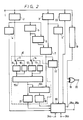
- Fig. 2 shows an overall or general arrangement of an apparatus for decoding BCH code according to an embodiment of the present invention.
- like parts corresponding to those of Fig. 1 are marked with the same references and therefore need not be described in detail.
- a Chien search circuit 8′ is constructed as shown in Fig. 2. More specifically, in the Chien search circuit 8′ of this embodiment, the adding circuit is divided to adding circuits 15a and 15b.
- the output of the adding circuit I5b is supplied to the zero detecting circuit 16.
- the signal of the result of operation from the adding circuit 15a is supplied to a zero detecting circuit 21.
- a correction instructing signal which the zero detecting circuit 21 generates as a high level signal when detecting (S1 ⁇ -2n + S12 ⁇ -n is supplied to the correcting signal and detecting signal generating circuit 30.
- the syndrome S1 from the S1 forming circuit 2 is supplied to a zero detecting circuit 4′ which generates, when the syndrome S1 is "O", a detecting signal as a low level signal. This detecting signal is supplied to the correcting signal and detecting signal generating circuit 30.
- the syndrome S3 from the S3 forming circuit 3 is supplied to a zero detecting circuit 4 ⁇ which generates, when detecting that the syndrome S3 is "O", a detecting signal as a low level signal. This detecting signal is supplied to the correcting signal and detecting signal generating circuit 30.
- the receiving sequence applied to the input terminal 1 is supplied to a parity forming circuit 23, and a parity detecting signal from the parity forming circuit 23 is supplied to the correcting signal and detecting signal generating circuit 30.
- the correcting signal and detecting signal generating circuit 30 is constructed as shown in Fig. 3.
- input terminals 31, 32, 33, 34, 35 and 36 are supplied with the detecting signals from the zero detecting circuit 4′, the zero detecting circuit 4 ⁇ , the parity forming circuit 23, the zero detecting circuit 21 and the zero detecting circuit 16, respectively.
- the input terminals 31 to 36 are connected to gate circuits, each forming a generating circuit. More specifically, the zero detecting signal of syndrome S1 at the input terminal 31 is supplied to one input terminal of a 2-input AND gate 37 which forms a one-bit error correcting signal generating circuit for (15, 11) BCH code in which the minimum distance is 3.
- the zero detecting signal for the added signal A from the adding circuit 15a and which is applied to the terminal 35 is supplied to the other input terminal of the AND gate 37.
- a logical product output from the AND gate 37 is supplied to a first fixed contact 61a of a first decoding change-over switch 61.
- the zero detecting signal of the syndrome S1 obtained at the terminal 31 is supplied to a first input terminal of 3-input AND circuit 38 forming a one-bit error correcting signal generating circuit for (15, 10) BCH code in which the minimum distance is 4.
- the parity detecting signal P obtained at the terminal 33 is supplied to a second input terminal of the AND gate 38.
- the zero detecting signal of the added signal A obtained at the terminal 35 is supplied to a third input terminal of the AND gate 38.
- the logical product output of the AND gate 38 is supplied to a first fixed contact 62a of a second decoding change-over switch 62.
- the zero detecting signal for the syndrome S1 obtained at the input terminal 31 is supplied to a first input terminal of a 3-input AND gate 39 forming a one-bit error correcting signal generating circuit for (15, 7) BCH code in which the minimum distance is 5.
- the zero detecting signal from the zero detecting circuit 22 for (S13 + S3) obtained at the input terminal 34 is supplied to a second input terminal of the AND gate 39.
- the zero detecting signal of the added signal B from the adding circuit 15b and developed at the input terminal 36 is supplied to a third input terminal of the AND gate 39. Then, the logical product output from the AND gate 39 is supplied to a first fixed contact 63a of a third decoding change-over switch 63.
- the zero detecting signal for the syndrome S1 obtained at the input terminal 31 is supplied to one input terminal of a 2-input AND gate 40 forming a two-bit error correcting signal generating circuit for (15, 7) BCH code in which the minimum distance is 5.
- the zero detecting signal of the added signal B derived from the adding circuit 15b and obtained at the input terminal 36 is supplied to the other input terminal of the AND gate 40.
- a logical product output from the AND gate 40 is supplied to a second fixed contact 63b of a third decoding change-over switch 63.
- the zero detecting signal of the syndrome S1 obtained at the input terminal 31 is supplied to a first input terminal of a 4-input AND gate 41 forming a one-bit error correcting signal generating circuit for (15, 6) BCH code in which the minimum distance is 6.
- the zero detecting signal for the zero detecting circuit 22 for (S13 + S3) and obtained at the input terminal 34 is supplied to a second input terminal of the AND gate 41.
- the parity detecting signal P obtained at the input terminal 33 is supplied to a third input terminal of the AND gate 41.
- the zero detecting signal for the added signal B derived from the adding circuit 15b and obtained at the input terminal 36 is supplied to a fourth input terminal of the AND gate 41. Then, a logical product output from the AND circuit 41 is supplied to a first fixed contact 64a of a fourth decoding change-over switch 64.
- the zero detecting signal for the syndrome S1 and obtained at the input terminal 31 is supplied to one input terminal of a 2-input AND gate 42 forming a two-bit error correcting signal generating circuit for (15, 6) BCH code in which the minimum distance is 6.
- the zero detecting signal for the added signal B derived from the adding circuit 15b and derived from the input terminal 36 is supplied to the other input terminal of the AND gate 42.
- a logical product output from the AND gate 42 is supplied to a second fixed contact 64b of the fourth decoding change-over switch 64.
- the correcting signal generating circuit is explaind so far, and the detecting signal generating circuit will be explained next.
- the zero detecting signal for the syndrome S1 obtained at the input terminal 31 is directlty supplied to a third fixed contact 65 of a fifth decoding change-over switch 65.
- the zero detecting signal for the syndrome S1 obtained at the terminal 31 is supplied to one input terminal of a 2-input AND gate 43 forming a 2-bit error detecting signal generating circuit for (15, 10) BCH code in which the minimum distance is 4.
- the parity detecting signal P obtained at the input terminal 33 is supplied to the other input terminal of the AND gate 43 through an inverter gate 44. Then, a logical product output of the AND gate 43 is supplied to a first fixed contact 66a of a sixth decoding change-over switch 66.
- the zero detecting signal for the syndrome S1 obtained at the input terminal 31 is supplied to one input terminal of a 2-input OR gate 45 forming a 3-bit error detecting signal generating circuit for (15, 10) BCH code in which the minimum distance is 4.
- the parity detecting signal P obtained at the input terminal 33 is supplied to the other input terminal of the OR gate 45.
- the logical sum output from the OR gate circuit 45 is supplied to a third fixed contact 66c of the sixth decoding change-over switch 66.
- the zero detecting signal derived from the zero detecting circuit 22 for (S13 + S3) and obtained at the input terminal 34 is supplied to a first fixed contact 67a of a seventh decoding change-over switch 67 through an inverter gate 46 forming a 2- and 3-bit error detecting signal generating circuit for (15, 7) BCH code in which the minimum distance is 5.
- the zero detecting signal for the syndrome S1 obtained at the input terminal 31 is supplied to a one input terminal of a 2-input OR gate 47 forming a 4-bit error detecting signal generating circuit for (15, 7) BCH code in which the minimum distance is 4.
- the zero detecting signal for the syndrome S3 obtained at the terminal 32 is supplied to the other input terminal of the OR gate 47.
- the logical sum output of the OR gate 47 is supplied to a third fixed contact 67c of the seventh decoding change-over switch 67.
- the zero detecting signal derived from the zero detecting circuit 22 for the (S13 + S3) and obtained at the terminal 34 is supplied through an inverter gate 48 to one input terminal of a 2-input AND gate 49 forming a 2-, 3-and 4-bit error detecting signal generating circuit for (15, 6) BCH code in which the minimum distance is 6.
- the zero detecting signals for the syndromes S1 and S3 obtained at the input terminals 31 and 32 are supplied to one input terminal and the other input terminal of a 2-input OR gate 50.
- the logical sum output of the OR gate 50 is supplied to the other input terminal of the AND gate 49.
- the logical product output of this AND gate 49 is supplied to a first fixed contact 68a of a eighth decoding change-over switch 68.
- the parity detecting signal P obtained at the terminal 33 is supplied to one input terminal of a 2-input AND gate 51 forming a 3-bit error detecting signal generating circuit for (15, 6) BCH code in which the minimum distance is 6.
- the zero detecting signal derived from the zero detecting circuit 22 for (S13 + S3) and obtained at the input terminal 34 is supplied to the other input terminal of the AND gate 51 through an inverter gate 52.
- the logical product output of the AND gate 51 is supplied to a second fixed contact 68b of the eighth decoding change-over switch 68.
- the zero detecting signal for the syndrome S1 obtained at the input terminal 31 is supplied to a first input terminal of a 3-input OR gate 53 forming a 5-bit error detecting signal generating circuit for (15, 6) BCH code in which the minimum distance is 6.
- the zero detecting signal for the syndrome S3 obtained at the input terminal 32 is supplied to a second input terminal of the OR gate 53, and the parity detecting signal P obtained at the terminal 33 is supplied to a third input terminal of the OR gate 53.
- a logical sum output from the OR gate 53 is supplied to a third fixed contact 68c of the eighth decoding change-over switch 68.
- the correcting signal and detecting signal generating circuit 30 is supplied with a decoding switching signal from a decoding switching signal input terminal 24a, and switching of the respective decoding change-over switches 61 to 68 is controlled by the decoding switching signal.
- the decoding change-over switches 61 to 68 connect their movable contacts 61m to 68m to their first fixed contacts 61a to 68a, respectively.
- the decoding change-over switches 61 to 68 connect their movable contacts 61m to 68m to their second fixed contacts 61b to 68b, respectively.
- the decoding change-over switches 61 to 68 connect their movable contacts 61m to 68m to their third fixed contacts 61c to 68c, respectively.
- Signals developed at the movable contacts 61m, 62m, 63m and 64m of the first, second, third and fourth decoding change-over switches 61, 62, 63 and 64 are supplied to first, second, third and fourth fixed contacts 71a, 71b, 71c and 71d of a first BCH change-over switch 71, and a signal developed at a movable contact 71m of the change-over switch 71 is supplied to a correcting signal output terminal 25a.
- Signals developed at movable contacts 65m, 66m, 67m and 68m of fifth, sixth, seventh and eighth decoding change-over switches 65, 66, 67 and 68 are supplied to first, second, third and fourth fixed contacts 72a, 72b, 72c and 72d of a second BCH change-over switch 72, and a signal developed at a movable contact 72m of the change-over switch 72 is supplied to a detecting signal output terminal 25b.
- the switching of the first and second BCH change-over switches 71 and 72 is controlled by a BCH switching signal which is supplied to the correcting signal and detecting signal generating circuit 30 from a BCH switching signal input terminal 24b.
- the BCH change-over switches 71 and 72 connect their movable contacts 71m and 72m to their first fixed contacts 71a and 72a, respectively.
- the BCH change-over switches 71 and 72 connect their movable contacts 71m and 72m to their second fixed contacts 71b and 72b, respectively.
- the BCH change-over switches 71 and 72 connect their movable contacts 71m and 72m to their third fixed contacts 71c and 72c, respectively.
- the BCH change-over switches 71 and 72 connect their movable contacts 71m and 72m to their fourth fixed contacts 71d and 72d, respectively.
- the error correcting signal obtained at the correcting signal output terminal 25a of the correcting signal and detecting signal generating circuit 30 in this embodiment is supplied to one input terminal of the 2-input EX-OR gate 18, and the output signal from the shift register 19 is supplied to the other input terminal of the EX-OR gate 18.
- the output signal from the EX-OR gate 18 is supplied to the output terminal 20, and data sequence thus error-corrected is derived from the output terminal 20.
- Other components of the decoding apparatus in this embodiment are formed similarly to those of the prior-art decoding apparatus of Fig. 1
- the apparatus for decoding BCH code can decode all BCH codes in which the minimum distance is 3 to 6, and, in which the elements over the Galois field which is given by (x4 + x + 1). A generator polynominal of each code will be explained below.
- the (15, 11) BCH code has the minimum distance of 3 and can correct the error of one bit or detect the errors of up to two bits.
- the (15, 10) BCH code resulting from expanding (15, 11) BCH code, has the minimum distance of 4. Therefore, the (15, 10) BCH code can correct one bit error and detect the errors up to 2 bits or detect the errors up to 3 bits.
- the (15, 7) BCH code has the minimum distance of 5 and can correct the errors up to 2 bits, or correct the error of one bit and detect the errors up to 3 bits or, alternatively, detect the errors up to 4 bits.
- the (15, 6) BCH code resulting from expanding the (15, 7) BCH code, has the minimum distance of 6, and therefore, the errors up to 2 bits can be corrected and the errors up to 3 bits can be detected or the error of one bit can be corrected and the errors up to 4 bits can be detected. Alternatively, the errors up to 5 bits can be detected.
- BCH code minimum distance is 3 0 0 1 ⁇ 0 2 ⁇ 0 (15, 10) BCH code: minimum distance is 4 0 0 0 1 ⁇ 0 1 2 ⁇ 0 0 3 not determined 1 (15, 7) BCH code: minimum distance is 5 0 0 0 0 1 ⁇ 0 ⁇ 0 0 2 ⁇ 0 not determined ⁇ 0 3 not determined ⁇ 0 ⁇ 0 4 not determined not determined not determined not determined not determined (15, 6) BCH code: minimum distance is 6 0 0 0 0 0 1 ⁇ 0 ⁇ 0 0 1 2 ⁇ 0 not determined ⁇ 0 0 3 not determined ⁇ 0 ⁇ 0 1 4 not determined not determined not determined not determined 0 5
- the correcing signal generating circuit and detecting signal generating circuit for the respective codes shown in Fig. 3 are constructed on the basis of the condition shown in Table 1.
- the switching signal for instructing one of the operations that the error of one bit is corrected, the errors of 2 bits are corrected and that the error is only detected is supplied to the terminal 24a and the switching signal instructing which one of the BCH codes is decoded is supplied to the terminal 24b, whereby all the decodings shown in Table 1 become possible. Therefore, the error correcting capability and the error detecting capability of BCH code of digital data to be transmitted can be changed by only switching the switches, and optimum BCH code can be selected on the basis of condition of transmission line, the kinds of transmission data and so on, which provides efficient data transmission.
- the circuit scale of the decoding apparatus is substantially the same as that of the prior-art decoding apparatus of Fig. 1, and is simple so that it can be formed as an LSI.
- the decoding apparatus of this embodiment can be applied to various decoding methods, and therefore, this decoding apparatus of the invention can be commonly applied to various transmitting apparatus.
- the decoder can be used for various purposes.
Landscapes
- Physics & Mathematics (AREA)
- Engineering & Computer Science (AREA)
- Theoretical Computer Science (AREA)
- Algebra (AREA)
- General Physics & Mathematics (AREA)
- Mathematical Physics (AREA)
- Pure & Applied Mathematics (AREA)
- Probability & Statistics with Applications (AREA)
- Error Detection And Correction (AREA)
Abstract
Description
- The present invention relates to an apparatus for decoding BCH code suitable for use in a wide variety of data communications.
- The assignee of the present application has previously proposed an apparatus for decoding BCH (Bose-Chaudhuri-Hocquenghem) code suitable for being formed as a large scale integrated (LSI) circuit (see Japanese Laid-open Patent Gazette No.61-281720, and corresponding U.S. Patent No. 4,751,704). This previously-proposed BCH code decoding apparatus is constructed as shown in Fig.
- In Fig. 1, a receiving sequence is applied to an
input terminal 1. The receiving sequence is supplied to an S1 forming circuit 2 and anS3 forming circuit 3 and the syndromes S1 and S3 are formed. The syndromes S1 and S3 are supplied to a zero detectingcircuit 4. The zero detectingcircuit 4 generates a detection signal of a low level "L" when all of the digits of the syndromes S1 and S3 are "O", namely, when no error is detected. This detection signal is supplied into alatch circuit 4A synchronously with the receiving sequence. - The syndrome S1 is supplied to an S1² forming circuit 5 and an
S1³ forming circuit 6 and the values of S1² and S1³ are produced. TheS1³ forming circuit 6 multiplies S1² with S1 to produce S1³ as will be explained hereinafter. The syndromes S3 and S1³ are supplied to an arithmetic operating circuit 7, by which (S1³ + S3) is formed. - In this manner, the respective coefficients S1, S1² s1³ and S3 of the error-location polynomial σ′(X) are obtained and supplied to a
Chien search circuit 8 for performing the process of Chien search. TheChien search circuit 8 is shown as the region surrounded by the broken line in Fig. 1 and comprises:arithmetic operating circuits 9 and 12;delay circuits circuits circuit 15; and a zero detectingcircuit 16. Theswitching circuits switching circuits delay circuits switching circuits - Outputs of the
switching circuits arithmetic operating circuits 9 and 12, respectively. Outputs of theoperating circuits 9 and 12 are supplied to thedelay circuits operating circuit 12 multiplies α⁻¹. α is the root of the generator polynomial over GF(2n). Assuming that a code length is n, the term of S1α-2n is obtained by the operating circuit 9 and the term of S1²α-n is derived by theoperating circuit 12. The outputs of theoperating circuits 9 and 12 are supplied to the addingcircuit 15 to perform the addition of 30 (mod. 2). - The adding
circuit 15 executes the arithmetic operation of the error-location polynomial (σ′(X) = S1x² + S1²x + S1³ + S3). An output of the addingcircuit 15 is supplied to the zero detectingcircuit 16. The position where the output of the addingcircuit 15 becomes zero is the error 5 location. The zero detectingcircuit 16 generates a correction instructing signal which becomes a high level "H" at the error location. - The correction instructing signal from the zero detecting
circuit 16 is supplied to anAND gate 17 together 10 with an output of thelatch circuit 4A. The output of thelatch circuit 4A becomes a low level "L", due to the zero detectingcircuit 4, when all digits of both of the syndromes S1 and S3 are "O". When (S1 = S3 = 0), the result of the operation of the error-location polynomial 15 becomes zero, so that the correction instructing signal which signals an error is generated from the zero detectingcircuit 16. TheAND gate 17 is provided to inhibit an improper correction instructing signal. - The correction instructing signal of "H" from the AND
gate 17 is supplied to an exclusive OR gate (hereinafter referred to as EX-OR gate) 18. The bits of the receiving sequence from ashift register 19 are inverted by the EX-ORgate 18 in response to the correction instructing signal which is generated in correspondence to the error location, so that the bit errors are corrected. The error-corrected data sequence from the EX-ORgate 18 is taken out to anoutput terminal 20. The shift register 19 delays the receiving sequence by the period of time necessary for 30 detection of the error location. - The invention can be applied to decode, for example, the (15, 7) BCH code, which (15) denotes the code length and (7) is the information bit length and the minimum distance is 5. Therefore, the errors of two bits or less can be corrected. The generator polynomial of this code is
G(x) = (x⁴ + x + 1) (x⁴ + x³ + x² + x + 1)
= x⁸ + x⁷ + x⁶ + x⁴ + 1
Assuming that α is the root of (x⁴ + x + 1 = 0), the minimal polynomial having α3 as the root is (x⁴ + x³ + x² + x + 1). The elements over the Galois Field GF(2⁴) which is given by (x⁴ + x + 1) = 0 are as follows.α³ α² α¹ α⁰ 0 0 0 0 0 0 0 0 0 1 α¹ 0 0 1 0 α² 0 1 0 0 α³ 1 0 0 0 α⁴ 0 0 1 1 α⁵ 0 1 1 0 α⁶ 1 1 0 0 α⁷ 1 0 1 1 α⁸ 0 1 0 1 α⁹ 1 0 1 0 α¹⁰ 0 1 1 1 α¹¹ 1 1 1 0 α¹² 1 1 1 1 α¹³ 1 1 0 1 α¹⁴ 1 0 0 1 - The parity-check matrix H of this code is shown below.

- The apparatus for decoding BCH code according to the 10 prior art can not alter error correction capability of error correction code.
- To solve this problem, it is proposed in the case of transmitting digital data that an error correction code of high redundancy is employed when a condition of
transmission 15 line is not good; and an error correction code of low redundancy is employed when a condition of transmission line is good. Thus, when the redundancy of error correction code is low, the remaining portion of the error correction code is used to transmit other digital data. - Depending on the kinds of information to be transmitted, it is requested either to increase error correction capability or to increase error detection capability even if the error correction capability is low. For example, when data for computer is transmitted, error 25 correction capability has to be increased because data for the computer needs accuracy. When digital audio data is transmitted, error detection capability has to be increased in order to compensate for data by interpolation of the preceding and succeeding data.
- If redundancy or capability of BCH code is changed, a plurality of decoding apparatus must be provided because the prior-art decoding apparatus of Fig. 1 decodes only one kind of BCH code. This provides a large-scaled arrangement of the apparatus.
- Accordingly, it is an object of the present invention to provide an improved apparatus for decoding BCH code in which the above defects encountered with the prior art can be eliminated.
- More specifically, it is another object of the present invention to provide an apparatus for decoding BCH code in which an error correction capability and an error detection capability of BCH code for digital data to be transmitted can be changed by switching change-over switches.
- It is still another object of the present invention to provide an apparatus for decoding BCH code in which a plurality of BCH codes can be decoded by a single decoding apparatus.
- According to an aspect of the present invention, there is provided an apparatus for decoding BCH code comprising:
- (a) first, second and third means for generating a syndrome S1, a syndrome S3 and a parity P, respectively from a receiving sequence;
- (b) fourth means coupled to said first means for generating S1² from the syndrome S1;
- (c) fifth means coupled to said first means, second means and fourth means for generating (S1³ + S3);
- (d) Chien search means including first generating means supplied with said S1 and S1² for generating a first stage of error-location polynomial A, wherein A = S1α-2n + S1²α-n, and second generating means supplied with said (S1³ + S3) and said A for generating a second stage of error-location polynomial B, wherein B = A + S1³ + S3; and
- (e) error correction logic means supplied with said S1, P, (S1³ + S3), A and B together with a decode selection signal and a BCH code selection signal for generating an error correction signal.
- These and other objects, features and advantages of the present invention will be apparent in the following detailed description of a preferred embodiment when read in conjunction with the accompanying drawings, in which like reference numerals are used to identify the same or similar parts in the several views.
-
- Fig. 1 is a functional block diagram showing an example of an apparatus for decoding BCH code according to the prior art;
- Fig. 2 is a functional block diagram showing an apparatus for decoding BCH code according to an embodiment of the present invention; and
- Fig. 3 is a block diagram of a circuit to generate an error correcting signal and an error detecting signal used in the apparatus of Fig. 2.
- An apparatus for decoding BCH code according to an embodiment of the present invention will hereinafter be described with reference to Figs. 2 and 3.
- Fig. 2 shows an overall or general arrangement of an apparatus for decoding BCH code according to an embodiment of the present invention. In Fig. 2, like parts corresponding to those of Fig. 1 are marked with the same references and therefore need not be described in detail.
- In the decoding apparatus of this embodiment, a
Chien search circuit 8′ is constructed as shown in Fig. 2. More specifically, in theChien search circuit 8′ of this embodiment, the adding circuit is divided to addingcircuits circuit 15a adds the output of the arithmetic operating circuit 9 and the output of thearithmetic operating circuit 12 and forms (A = S1α-2n + S1² α-n). The addingcircuit 15b adds the output of the addingcircuit 15a and the output of the arithmetic operating circuit 7 and forms (B = A + S1³ + S3). The output of the adding circuit I5b is supplied to the zero detectingcircuit 16. The correction instructing signal which the zero detectingcircuit 16 produces as a high level signal when detecting (A + S1³ + S3 = 0) is supplied to a correcting signal and detectingsignal generating circuit 30. - The signal of the result of operation from the adding
circuit 15a is supplied to a zero detectingcircuit 21. A correction instructing signal which the zero detectingcircuit 21 generates as a high level signal when detecting (S1α-2n + S1²α-n is supplied to the correcting signal and detectingsignal generating circuit 30. - The syndrome S1 from the S1 forming circuit 2 is supplied to a zero detecting
circuit 4′ which generates, when the syndrome S1 is "O", a detecting signal as a low level signal. This detecting signal is supplied to the correcting signal and detectingsignal generating circuit 30. The syndrome S3 from theS3 forming circuit 3 is supplied to a zero detectingcircuit 4˝ which generates, when detecting that the syndrome S3 is "O", a detecting signal as a low level signal. This detecting signal is supplied to the correcting signal and detectingsignal generating circuit 30. - The receiving sequence applied to the
input terminal 1 is supplied to aparity forming circuit 23, and a parity detecting signal from theparity forming circuit 23 is supplied to the correcting signal and detectingsignal generating circuit 30. - The correcting signal and detecting
signal generating circuit 30 is constructed as shown in Fig. 3. - As shown in Fig. 3,
input terminals circuit 4′, the zero detectingcircuit 4˝, theparity forming circuit 23, the zero detectingcircuit 21 and the zero detectingcircuit 16, respectively. - The
input terminals 31 to 36 are connected to gate circuits, each forming a generating circuit. More specifically, the zero detecting signal of syndrome S1 at theinput terminal 31 is supplied to one input terminal of a 2-input ANDgate 37 which forms a one-bit error correcting signal generating circuit for (15, 11) BCH code in which the minimum distance is 3. The zero detecting signal for the added signal A from the addingcircuit 15a and which is applied to the terminal 35 is supplied to the other input terminal of the ANDgate 37. A logical product output from the ANDgate 37 is supplied to a firstfixed contact 61a of a first decoding change-over switch 61. - The zero detecting signal of the syndrome S1 obtained at the terminal 31 is supplied to a first input terminal of 3-input AND
circuit 38 forming a one-bit error correcting signal generating circuit for (15, 10) BCH code in which the minimum distance is 4. The parity detecting signal P obtained at the terminal 33 is supplied to a second input terminal of the ANDgate 38. The zero detecting signal of the added signal A obtained at the terminal 35 is supplied to a third input terminal of the ANDgate 38. The logical product output of the ANDgate 38 is supplied to a firstfixed contact 62a of a second decoding change-over switch 62. - The zero detecting signal for the syndrome S1 obtained at the
input terminal 31 is supplied to a first input terminal of a 3-input ANDgate 39 forming a one-bit error correcting signal generating circuit for (15, 7) BCH code in which the minimum distance is 5. The zero detecting signal from the zero detectingcircuit 22 for (S1³ + S3) obtained at theinput terminal 34 is supplied to a second input terminal of the ANDgate 39. The zero detecting signal of the added signal B from the addingcircuit 15b and developed at theinput terminal 36 is supplied to a third input terminal of the ANDgate 39. Then, the logical product output from the ANDgate 39 is supplied to a firstfixed contact 63a of a third decoding change-over switch 63. - The zero detecting signal for the syndrome S1 obtained at the
input terminal 31 is supplied to one input terminal of a 2-input AND gate 40 forming a two-bit error correcting signal generating circuit for (15, 7) BCH code in which the minimum distance is 5. The zero detecting signal of the added signal B derived from the addingcircuit 15b and obtained at theinput terminal 36 is supplied to the other input terminal of the AND gate 40. Then, a logical product output from the AND gate 40 is supplied to a secondfixed contact 63b of a third decoding change-over switch 63. - The zero detecting signal of the syndrome S1 obtained at the
input terminal 31 is supplied to a first input terminal of a 4-input ANDgate 41 forming a one-bit error correcting signal generating circuit for (15, 6) BCH code in which the minimum distance is 6. The zero detecting signal for the zero detectingcircuit 22 for (S1³ + S3) and obtained at theinput terminal 34 is supplied to a second input terminal of the ANDgate 41. The parity detecting signal P obtained at theinput terminal 33 is supplied to a third input terminal of the ANDgate 41. The zero detecting signal for the added signal B derived from the addingcircuit 15b and obtained at theinput terminal 36 is supplied to a fourth input terminal of the ANDgate 41. Then, a logical product output from the ANDcircuit 41 is supplied to a firstfixed contact 64a of a fourth decoding change-over switch 64. - The zero detecting signal for the syndrome S1 and obtained at the
input terminal 31 is supplied to one input terminal of a 2-input ANDgate 42 forming a two-bit error correcting signal generating circuit for (15, 6) BCH code in which the minimum distance is 6. The zero detecting signal for the added signal B derived from the addingcircuit 15b and derived from theinput terminal 36 is supplied to the other input terminal of the ANDgate 42. Then, a logical product output from the ANDgate 42 is supplied to a secondfixed contact 64b of the fourth decoding change-over switch 64. - The correcting signal generating circuit is explaind so far, and the detecting signal generating circuit will be explained next.
- The zero detecting signal for the syndrome S1 obtained at the
input terminal 31 is directlty supplied to a thirdfixed contact 65 of a fifth decoding change-over switch 65. - The zero detecting signal for the syndrome S1 obtained at the terminal 31 is supplied to one input terminal of a 2-input AND
gate 43 forming a 2-bit error detecting signal generating circuit for (15, 10) BCH code in which the minimum distance is 4. The parity detecting signal P obtained at theinput terminal 33 is supplied to the other input terminal of the ANDgate 43 through aninverter gate 44. Then, a logical product output of the ANDgate 43 is supplied to a first fixed contact 66a of a sixth decoding change-over switch 66. - The zero detecting signal for the syndrome S1 obtained at the
input terminal 31 is supplied to one input terminal of a 2-input ORgate 45 forming a 3-bit error detecting signal generating circuit for (15, 10) BCH code in which the minimum distance is 4. The parity detecting signal P obtained at theinput terminal 33 is supplied to the other input terminal of theOR gate 45. The logical sum output from theOR gate circuit 45 is supplied to a thirdfixed contact 66c of the sixth decoding change-over switch 66. - The zero detecting signal derived from the zero detecting
circuit 22 for (S1³ + S3) and obtained at theinput terminal 34 is supplied to a firstfixed contact 67a of a seventh decoding change-over switch 67 through aninverter gate 46 forming a 2- and 3-bit error detecting signal generating circuit for (15, 7) BCH code in which the minimum distance is 5. - The zero detecting signal for the syndrome S1 obtained at the
input terminal 31 is supplied to a one input terminal of a 2-input ORgate 47 forming a 4-bit error detecting signal generating circuit for (15, 7) BCH code in which the minimum distance is 4. The zero detecting signal for the syndrome S3 obtained at the terminal 32 is supplied to the other input terminal of theOR gate 47. The logical sum output of theOR gate 47 is supplied to a thirdfixed contact 67c of the seventh decoding change-over switch 67. - The zero detecting signal derived from the zero detecting
circuit 22 for the (S1³ + S3) and obtained at the terminal 34 is supplied through aninverter gate 48 to one input terminal of a 2-input ANDgate 49 forming a 2-, 3-and 4-bit error detecting signal generating circuit for (15, 6) BCH code in which the minimum distance is 6. The zero detecting signals for the syndromes S1 and S3 obtained at theinput terminals gate 50. The logical sum output of theOR gate 50 is supplied to the other input terminal of the ANDgate 49. The logical product output of this ANDgate 49 is supplied to a firstfixed contact 68a of a eighth decoding change-over switch 68. - The parity detecting signal P obtained at the terminal 33 is supplied to one input terminal of a 2-input AND gate 51 forming a 3-bit error detecting signal generating circuit for (15, 6) BCH code in which the minimum distance is 6. The zero detecting signal derived from the zero detecting
circuit 22 for (S1³ + S3) and obtained at theinput terminal 34 is supplied to the other input terminal of the AND gate 51 through aninverter gate 52. The logical product output of the AND gate 51 is supplied to a second fixed contact 68b of the eighth decoding change-over switch 68. - The zero detecting signal for the syndrome S1 obtained at the
input terminal 31 is supplied to a first input terminal of a 3-input ORgate 53 forming a 5-bit error detecting signal generating circuit for (15, 6) BCH code in which the minimum distance is 6. The zero detecting signal for the syndrome S3 obtained at theinput terminal 32 is supplied to a second input terminal of theOR gate 53, and the parity detecting signal P obtained at the terminal 33 is supplied to a third input terminal of theOR gate 53. A logical sum output from theOR gate 53 is supplied to a thirdfixed contact 68c of the eighth decoding change-over switch 68. - The correcting signal and detecting
signal generating circuit 30 according to this embodiment is supplied with a decoding switching signal from a decoding switchingsignal input terminal 24a, and switching of the respective decoding change-overswitches 61 to 68 is controlled by the decoding switching signal. - More specifically, when a signal instructing one-bit correction is supplied to the
input terminal 24a, the decoding change-overswitches 61 to 68 connect theirmovable contacts 61m to 68m to their first fixedcontacts 61a to 68a, respectively. When a signal instructing a two-bit correction is supplied to theinput terminal 24a, the decoding change-overswitches 61 to 68 connect theirmovable contacts 61m to 68m to their second fixedcontacts 61b to 68b, respectively. Further, when an error detection instructing signal is supplied to theinput terminal 24a, the decoding change-overswitches 61 to 68 connect theirmovable contacts 61m to 68m to their thirdfixed contacts 61c to 68c, respectively. - Signals developed at the
movable contacts switches fixed contacts over switch 71, and a signal developed at amovable contact 71m of the change-over switch 71 is supplied to a correctingsignal output terminal 25a. - Signals developed at
movable contacts switches fixed contacts signal output terminal 25b. In this case the switching of the first and second BCH change-overswitches 71 and 72 is controlled by a BCH switching signal which is supplied to the correcting signal and detectingsignal generating circuit 30 from a BCH switchingsignal input terminal 24b. More specifically, when a signal instructing (15, 11) BCH switching signal is supplied to the terminal 24b, the BCH change-overswitches 71 and 72 connect theirmovable contacts 71m and 72m to their first fixedcontacts switches 71 and 72 connect theirmovable contacts 71m and 72m to their second fixedcontacts 71b and 72b, respectively. When a signal instructing (15, 7) BCH code is supplied to the terminal 24b, the BCH change-overswitches 71 and 72 connect theirmovable contacts 71m and 72m to their thirdfixed contacts switches 71 and 72 connect theirmovable contacts 71m and 72m to their fourth fixedcontacts - Referring back to Fig. 2, the error correcting signal obtained at the correcting
signal output terminal 25a of the correcting signal and detectingsignal generating circuit 30 in this embodiment is supplied to one input terminal of the 2-input EX-OR gate 18, and the output signal from theshift register 19 is supplied to the other input terminal of theEX-OR gate 18. The output signal from theEX-OR gate 18 is supplied to theoutput terminal 20, and data sequence thus error-corrected is derived from theoutput terminal 20. Other components of the decoding apparatus in this embodiment are formed similarly to those of the prior-art decoding apparatus of Fig. 1 - BCH code, decoded by the decoding apparatus of the invention, will be explained hereinbelow.
- The apparatus for decoding BCH code according to this embodiment can decode all BCH codes in which the minimum distance is 3 to 6, and, in which the elements over the Galois field which is given by (x⁴ + x + 1). A generator polynominal of each code will be explained below.
- The (15, 11) BCH code has the minimum distance of 3 and can correct the error of one bit or detect the errors of up to two bits. The generator polynomial of this code is
G₁(X) = x⁴ + x + 1 - The (15, 10) BCH code, resulting from expanding (15, 11) BCH code, has the minimum distance of 4. Therefore, the (15, 10) BCH code can correct one bit error and detect the errors up to 2 bits or detect the errors up to 3 bits. The generator polynomial of this code is
G₂(X) = (x⁴ + x + 1) (x + 1)
= x⁵ + x⁴ + x² + x - The (15, 7) BCH code has the minimum distance of 5 and can correct the errors up to 2 bits, or correct the error of one bit and detect the errors up to 3 bits or, alternatively, detect the errors up to 4 bits. The generator polynomial of this code is
G₃(X) = (x⁴ + x + 1) (x⁴ + x³ + x² + x + 1)
= x⁸ + x⁷ + x⁶ + x⁴ + 1 - The (15, 6) BCH code, resulting from expanding the (15, 7) BCH code, has the minimum distance of 6, and therefore, the errors up to 2 bits can be corrected and the errors up to 3 bits can be detected or the error of one bit can be corrected and the errors up to 4 bits can be detected. Alternatively, the errors up to 5 bits can be detected. The generator polynomial of this code is
G₄(X) = (x⁴ + x + 1) (x⁴ + x³ + x² + x + 1) (x + 1)
= x⁹ + x⁶ + x⁵ + x⁴ + x + 1 - The following table 1 show conditions of the respective detecting signals which are supplied to the above correcting signal and detecting
signal generating circuit 30 on the basis of the number of errors in the application of BCH codes.TABLE 1 BCH Codes Number of errors S1 S3 S1³ + S3 P (15, 11) BCH code: minimum distance is 3 0 0 1 ≠ 0 2 ≠ 0 (15, 10) BCH code: minimum distance is 4 0 0 0 1 ≠ 0 1 2 ≠ 0 0 3 not determined 1 (15, 7) BCH code: minimum distance is 5 0 0 0 0 1 ≠ 0 ≠ 0 0 2 ≠ 0 not determined ≠ 0 3 not determined ≠ 0 ≠ 0 4 not determined not determined not determined (15, 6) BCH code: minimum distance is 6 0 0 0 0 0 1 ≠ 0 ≠ 0 0 1 2 ≠ 0 not determined ≠ 0 0 3 not determined ≠ 0 ≠ 0 1 4 not determined not determined not determined 0 5 not determined not determined not determined 1 - When the number of errors of the (15, 7) BCH code is four and the number of errors of the (15, 6) BCH code is four, the syndromes S1 and S3 do not become zero simultaneously.
- The correcing signal generating circuit and detecting signal generating circuit for the respective codes shown in Fig. 3 are constructed on the basis of the condition shown in Table 1. The switching signal for instructing one of the operations that the error of one bit is corrected, the errors of 2 bits are corrected and that the error is only detected is supplied to the terminal 24a and the switching signal instructing which one of the BCH codes is decoded is supplied to the terminal 24b, whereby all the decodings shown in Table 1 become possible. Therefore, the error correcting capability and the error detecting capability of BCH code of digital data to be transmitted can be changed by only switching the switches, and optimum BCH code can be selected on the basis of condition of transmission line, the kinds of transmission data and so on, which provides efficient data transmission. Further, in this embodiment, the circuit scale of the decoding apparatus is substantially the same as that of the prior-art decoding apparatus of Fig. 1, and is simple so that it can be formed as an LSI.
- Furthermore, the decoding apparatus of this embodiment can be applied to various decoding methods, and therefore, this decoding apparatus of the invention can be commonly applied to various transmitting apparatus. Thus, the decoder can be used for various purposes.
- Having described a preferred embodiment in detail with reference to the accompanying drawings, it is to be understood that the present invention is not limited to that precise embodiment and that many changes and modifications could be effected by one skilled in the art without departing from the spirit and scope of the invention as defined in the appended claims.
Claims (5)
Applications Claiming Priority (2)
| Application Number | Priority Date | Filing Date | Title |
|---|---|---|---|
| JP278722/88 | 1988-11-04 | ||
| JP63278722A JPH02125532A (en) | 1988-11-04 | 1988-11-04 | Decoder for bch code |
Publications (3)
| Publication Number | Publication Date |
|---|---|
| EP0367268A2 true EP0367268A2 (en) | 1990-05-09 |
| EP0367268A3 EP0367268A3 (en) | 1991-05-22 |
| EP0367268B1 EP0367268B1 (en) | 1995-09-06 |
Family
ID=17601287
Family Applications (1)
| Application Number | Title | Priority Date | Filing Date |
|---|---|---|---|
| EP89120308A Expired - Lifetime EP0367268B1 (en) | 1988-11-04 | 1989-11-02 | Apparatus for decoding BCH code |
Country Status (5)
| Country | Link |
|---|---|
| US (1) | US5208815A (en) |
| EP (1) | EP0367268B1 (en) |
| JP (1) | JPH02125532A (en) |
| KR (1) | KR900008785A (en) |
| DE (1) | DE68924124T2 (en) |
Cited By (3)
| Publication number | Priority date | Publication date | Assignee | Title |
|---|---|---|---|---|
| FR2717968A1 (en) * | 1994-03-25 | 1995-09-29 | Mitsubishi Electric Corp | Encoder performing error correction, decoder performing error correction and data transmission system using error correction codes. |
| EP0660533A3 (en) * | 1993-12-20 | 1996-01-03 | At & T Corp | Method and apparatus for a reduced iteration decoder. |
| US5912905A (en) * | 1994-03-25 | 1999-06-15 | Mitsubishi Denki Kabushiki Kaisha | Error-correcting encoder, error-correcting decoder and data transmitting system with error-correcting codes |
Families Citing this family (9)
| Publication number | Priority date | Publication date | Assignee | Title |
|---|---|---|---|---|
| DE4105860C2 (en) * | 1991-02-25 | 1995-04-20 | Broadcast Television Syst | Circuit arrangement for recognizing and correcting errors in data words |
| JP2824474B2 (en) * | 1992-02-17 | 1998-11-11 | 三菱電機株式会社 | Error correction system and decoder using this error correction system |
| EP0563491A1 (en) * | 1992-03-31 | 1993-10-06 | International Business Machines Corporation | Method and apparatus for implementing a triple error detection and double error correction code |
| US5373511A (en) * | 1992-05-04 | 1994-12-13 | Motorola, Inc. | Method for decoding a reed solomon encoded signal with inner code and apparatus for doing same |
| US5822339A (en) * | 1996-05-30 | 1998-10-13 | Rockwell International | Data decoder and method to correct inversions or phase ambiguity for M-ary transmitted data |
| JP4846384B2 (en) * | 2006-02-20 | 2011-12-28 | 株式会社東芝 | Semiconductor memory device |
| JP2007305267A (en) * | 2006-05-15 | 2007-11-22 | Toshiba Corp | Semiconductor storage device |
| KR101437396B1 (en) * | 2008-02-27 | 2014-09-05 | 삼성전자주식회사 | A memory system including an error correction block capable of reducing latency and an error correction method thereof |
| TWI551059B (en) * | 2014-07-11 | 2016-09-21 | 衡宇科技股份有限公司 | MULTI-CODE CHIEN'S SEARCH CIRCUIT FOR BCH CODES WITH VARIOUS VALUES OF M IN GF(2m) |
Family Cites Families (18)
| Publication number | Priority date | Publication date | Assignee | Title |
|---|---|---|---|---|
| US3078443A (en) * | 1959-01-22 | 1963-02-19 | Alan C Rose | Compound error correction system |
| US3418629A (en) * | 1964-04-10 | 1968-12-24 | Ibm | Decoders for cyclic error-correcting codes |
| US3372376A (en) * | 1964-10-05 | 1968-03-05 | Bell Telephone Labor Inc | Error control apparatus |
| US3411135A (en) * | 1965-03-15 | 1968-11-12 | Bell Telephone Labor Inc | Error control decoding system |
| US3623155A (en) * | 1969-12-24 | 1971-11-23 | Ibm | Optimum apparatus and method for check bit generation and error detection, location and correction |
| GB1389551A (en) * | 1972-05-15 | 1975-04-03 | Secr Defence | Multiplex digital telecommunications apparatus having error- correcting facilities |
| US4107652A (en) * | 1975-12-27 | 1978-08-15 | Fujitsu Limited | Error correcting and controlling system |
| US4397022A (en) * | 1981-01-30 | 1983-08-02 | Weng Ming I | Weighted erasure codec for the (24, 12) extended Golay code |
| US4556977A (en) * | 1983-09-15 | 1985-12-03 | International Business Machines Corporation | Decoding of BCH double error correction - triple error detection (DEC-TED) codes |
| JPS6162234A (en) * | 1984-09-04 | 1986-03-31 | Kokusai Denshin Denwa Co Ltd <Kdd> | Error correction code decoding system |
| US4739504A (en) * | 1985-06-03 | 1988-04-19 | Unisys Corp. | IC chip error detecting and correcting method |
| US4739506A (en) * | 1985-06-03 | 1988-04-19 | Unisys Corp. | IC chip error detecting and correcting apparatus |
| JPH0728227B2 (en) * | 1985-06-07 | 1995-03-29 | ソニー株式会社 | Decoding device for BCH code |
| US4723245A (en) * | 1985-07-01 | 1988-02-02 | Unisys Corporation | IC chip error detecting and correcting method including automatic self-checking of chip operation |
| US4771429A (en) * | 1986-09-18 | 1988-09-13 | Abbott Laboratories | Circuit combining functions of cyclic redundancy check code and pseudo-random number generators |
| US4833678A (en) * | 1987-07-22 | 1989-05-23 | Cyclotomics, Inc. | Hard-wired serial Galois field decoder |
| US4890286A (en) * | 1987-12-11 | 1989-12-26 | Sanyo Electric Co., Ltd. | Method and apparatus for decoding error correcting code |
| JP2881773B2 (en) * | 1988-07-30 | 1999-04-12 | ソニー株式会社 | Error correction device |
-
1988
- 1988-11-04 JP JP63278722A patent/JPH02125532A/en active Pending
-
1989
- 1989-10-26 US US07/426,862 patent/US5208815A/en not_active Expired - Fee Related
- 1989-11-01 KR KR1019890015786A patent/KR900008785A/en not_active Ceased
- 1989-11-02 EP EP89120308A patent/EP0367268B1/en not_active Expired - Lifetime
- 1989-11-02 DE DE68924124T patent/DE68924124T2/en not_active Expired - Fee Related
Cited By (5)
| Publication number | Priority date | Publication date | Assignee | Title |
|---|---|---|---|---|
| EP0660533A3 (en) * | 1993-12-20 | 1996-01-03 | At & T Corp | Method and apparatus for a reduced iteration decoder. |
| FR2717968A1 (en) * | 1994-03-25 | 1995-09-29 | Mitsubishi Electric Corp | Encoder performing error correction, decoder performing error correction and data transmission system using error correction codes. |
| US5699368A (en) * | 1994-03-25 | 1997-12-16 | Mitsubishi Denki Kabushiki Kaisha | Error-correcting encoder, error-correcting decoder, and data transmitting system with error-correcting codes |
| US5912905A (en) * | 1994-03-25 | 1999-06-15 | Mitsubishi Denki Kabushiki Kaisha | Error-correcting encoder, error-correcting decoder and data transmitting system with error-correcting codes |
| DE19509728B4 (en) * | 1994-03-25 | 2005-09-22 | Mitsubishi Denki K.K. | Method for coding information symbols, error correcting decoder, error correcting apparatus for coding and decoding, and decoding method |
Also Published As
| Publication number | Publication date |
|---|---|
| KR900008785A (en) | 1990-06-04 |
| DE68924124D1 (en) | 1995-10-12 |
| EP0367268A3 (en) | 1991-05-22 |
| US5208815A (en) | 1993-05-04 |
| JPH02125532A (en) | 1990-05-14 |
| DE68924124T2 (en) | 1996-02-01 |
| EP0367268B1 (en) | 1995-09-06 |
Similar Documents
| Publication | Publication Date | Title |
|---|---|---|
| EP0147041B1 (en) | Error protection apparatus | |
| US4555784A (en) | Parity and syndrome generation for error detection and correction in digital communication systems | |
| EP0278383B1 (en) | Error correction method using reed-solomon code | |
| US5040179A (en) | High data rate BCH encoder | |
| US4504948A (en) | Syndrome processing unit for multibyte error correcting systems | |
| EP0233075B1 (en) | Method and apparatus for generating error detection check bytes for a data record | |
| EP0367268A2 (en) | Apparatus for decoding BCH code | |
| KR970706655A (en) | Multi-purpose error correction system (VERSATILE ERROR CORRECTION SYSTEM) | |
| EP0061345B1 (en) | Processing circuits for operating on digital data words which are elements of a galois field | |
| US5748652A (en) | Apparatus for detecting and correcting cyclic redundancy check errors | |
| US3728678A (en) | Error-correcting systems utilizing rate {178 {11 diffuse codes | |
| Okano et al. | A construction method of high-speed decoders using ROM's for Bose–Chaudhuri–Hocquenghem and Reed–Solomon codes | |
| JPH07312560A (en) | Error correction coder, error correction decoder, data transmission system with error correction code and decoding method for error correction code | |
| CA1256202A (en) | Method and apparatus for decoding bch code | |
| US5936978A (en) | Shortened fire code error-trapping decoding method and apparatus | |
| US3771126A (en) | Error correction for self-synchronized scramblers | |
| US7093183B2 (en) | Symbol level error correction codes which protect against memory chip and bus line failures | |
| EP0806838A1 (en) | Polynomial evaluator for use in a reed-solomon decoder | |
| US4453249A (en) | System for binary data transmission | |
| JPH06276106A (en) | Error correcting/decoding device | |
| JPH0345020A (en) | Cyclic code processing circuit | |
| US20070033507A1 (en) | Efficient error code correction | |
| JPH0482325A (en) | Error correction device for bch code | |
| KR100407131B1 (en) | Reed solomon decoder using combinational circuits | |
| JPS60233938A (en) | Error correction coder |
Legal Events
| Date | Code | Title | Description |
|---|---|---|---|
| PUAI | Public reference made under article 153(3) epc to a published international application that has entered the european phase |
Free format text: ORIGINAL CODE: 0009012 |
|
| AK | Designated contracting states |
Kind code of ref document: A2 Designated state(s): DE FR GB NL |
|
| PUAL | Search report despatched |
Free format text: ORIGINAL CODE: 0009013 |
|
| AK | Designated contracting states |
Kind code of ref document: A3 Designated state(s): DE FR GB NL |
|
| 17P | Request for examination filed |
Effective date: 19910715 |
|
| 17Q | First examination report despatched |
Effective date: 19931129 |
|
| GRAA | (expected) grant |
Free format text: ORIGINAL CODE: 0009210 |
|
| AK | Designated contracting states |
Kind code of ref document: B1 Designated state(s): DE FR GB NL |
|
| REF | Corresponds to: |
Ref document number: 68924124 Country of ref document: DE Date of ref document: 19951012 |
|
| ET | Fr: translation filed | ||
| PLBE | No opposition filed within time limit |
Free format text: ORIGINAL CODE: 0009261 |
|
| STAA | Information on the status of an ep patent application or granted ep patent |
Free format text: STATUS: NO OPPOSITION FILED WITHIN TIME LIMIT |
|
| 26N | No opposition filed | ||
| PGFP | Annual fee paid to national office [announced via postgrant information from national office to epo] |
Ref country code: GB Payment date: 19971024 Year of fee payment: 9 |
|
| PGFP | Annual fee paid to national office [announced via postgrant information from national office to epo] |
Ref country code: DE Payment date: 19971110 Year of fee payment: 9 |
|
| PGFP | Annual fee paid to national office [announced via postgrant information from national office to epo] |
Ref country code: FR Payment date: 19971112 Year of fee payment: 9 |
|
| PGFP | Annual fee paid to national office [announced via postgrant information from national office to epo] |
Ref country code: NL Payment date: 19971130 Year of fee payment: 9 |
|
| PG25 | Lapsed in a contracting state [announced via postgrant information from national office to epo] |
Ref country code: GB Free format text: LAPSE BECAUSE OF NON-PAYMENT OF DUE FEES Effective date: 19981102 |
|
| PG25 | Lapsed in a contracting state [announced via postgrant information from national office to epo] |
Ref country code: NL Free format text: LAPSE BECAUSE OF NON-PAYMENT OF DUE FEES Effective date: 19990601 |
|
| GBPC | Gb: european patent ceased through non-payment of renewal fee |
Effective date: 19981102 |
|
| PG25 | Lapsed in a contracting state [announced via postgrant information from national office to epo] |
Ref country code: FR Free format text: LAPSE BECAUSE OF NON-PAYMENT OF DUE FEES Effective date: 19990730 |
|
| NLV4 | Nl: lapsed or anulled due to non-payment of the annual fee |
Effective date: 19990601 |
|
| REG | Reference to a national code |
Ref country code: FR Ref legal event code: ST |
|
| PG25 | Lapsed in a contracting state [announced via postgrant information from national office to epo] |
Ref country code: DE Free format text: LAPSE BECAUSE OF NON-PAYMENT OF DUE FEES Effective date: 19990901 |