EP0366552B1 - Procédé pour fabriquer un transistor bipolaire du type hétérojonction - Google Patents
Procédé pour fabriquer un transistor bipolaire du type hétérojonction Download PDFInfo
- Publication number
- EP0366552B1 EP0366552B1 EP89402953A EP89402953A EP0366552B1 EP 0366552 B1 EP0366552 B1 EP 0366552B1 EP 89402953 A EP89402953 A EP 89402953A EP 89402953 A EP89402953 A EP 89402953A EP 0366552 B1 EP0366552 B1 EP 0366552B1
- Authority
- EP
- European Patent Office
- Prior art keywords
- layer
- base layer
- growing
- beryllium
- base
- Prior art date
- Legal status (The legal status is an assumption and is not a legal conclusion. Google has not performed a legal analysis and makes no representation as to the accuracy of the status listed.)
- Expired - Lifetime
Links
Images


Classifications
-
- H—ELECTRICITY
- H10—SEMICONDUCTOR DEVICES; ELECTRIC SOLID-STATE DEVICES NOT OTHERWISE PROVIDED FOR
- H10D—INORGANIC ELECTRIC SEMICONDUCTOR DEVICES
- H10D10/00—Bipolar junction transistors [BJT]
- H10D10/01—Manufacture or treatment
- H10D10/021—Manufacture or treatment of heterojunction BJTs [HBT]
-
- H—ELECTRICITY
- H10—SEMICONDUCTOR DEVICES; ELECTRIC SOLID-STATE DEVICES NOT OTHERWISE PROVIDED FOR
- H10P—GENERIC PROCESSES OR APPARATUS FOR THE MANUFACTURE OR TREATMENT OF DEVICES COVERED BY CLASS H10
- H10P32/00—Diffusion of dopants within, into or out of wafers, substrates or parts of devices
-
- H—ELECTRICITY
- H10—SEMICONDUCTOR DEVICES; ELECTRIC SOLID-STATE DEVICES NOT OTHERWISE PROVIDED FOR
- H10D—INORGANIC ELECTRIC SEMICONDUCTOR DEVICES
- H10D62/00—Semiconductor bodies, or regions thereof, of devices having potential barriers
- H10D62/80—Semiconductor bodies, or regions thereof, of devices having potential barriers characterised by the materials
- H10D62/85—Semiconductor bodies, or regions thereof, of devices having potential barriers characterised by the materials being Group III-V materials, e.g. GaAs
Definitions
- the present invention generally relates to semiconductor devices and more particularly to a method of manufacturing a heterojunction bipolar transistor (HBT).
- HBT heterojunction bipolar transistor
- HBT using a group III-V compound semiconductor material such as gallium arsenide (GaAs) is characterized by a high operational speed.
- This desirable operational characteristic is obtained mainly as a result of the high electron mobility in the the group III-V compound forming the transistor.
- the use of a material having a large band gap for the emitter also contributes to the increase of the speed of the device.
- the base of the transistor is made as thin as possible in order to reduce the base transit time of electron and hence to increase the operational speed of the transistor further.
- excessive reduction of the thickness of the base causes an adverse increase of the base spreading resistance which in turn decreases the speed of the transistor.
- the operational speed of the HBT is further improved by establishing an electric field in the base such that the electron passing therethrough is accelerated.
- Such an electric field is obtained by providing a compositional gradient in the material forming the base such that there is a large band gap at a side of the base in contact with the emitter and such that the band gap is narrowed continuously toward the collector.
- gallium aluminium arsenide (GaAlAs) having a composition of Ga 1-x Al x As is used for the base with a gradual change of the composition x ranging from 0 to 0.1. Note that there is substantially no change of lattice constant in the foregoing system and the problem of the lattice mismatch is avoided.
- Be beryllium
- the diffusion coefficient of Be in GaAs increases steeply by a factor of one thousand to even ten thousand when the concentration level of Be is increased beyond a level of about 4 X 1019 cm ⁇ 3 (Pao, Y.C. et al. J. Appl. Phys. 60 , 1986, p.201).
- such an increase of the diffusion coefficient of Be is further enhanced in the system of GaAlAs (Miller, D.L., J. Appl. Phys.
- the conventional HBT has a problem in that it cannot be constructed to have a sufficiently reduced base thickness as well as a graded base profile to fully exploit the high speed performance of the HBT.
- npn-type HBT is constructed on an indium phosphide (InP) substrate with a base of indium gallium aluminium arsenide (InGaAlAs) sandwiched by a collector and an emitter of indium gallium arsenide.
- InP indium phosphide
- InGaAlAs indium gallium aluminium arsenide
- Be is doped to a level exceeding about 1 X 1020cm ⁇ 3 in InGaAlAs, the diffusion coefficient of Be is increased significantly.
- This device does not allow the compositional gradient in the base and thus the device has a limitation in the operational speed. Formation of the compositional gradation by adding elements other than Al to the system of InGaAs is generally not possible because of the unacceptable mismatch of lattice with respect to the collector or emitter.
- Another and more specific object of the present invention is to provide a method of manufacturing a semiconductor device having an epitaxial layer of a compound semiconductor material containing Be with a high concentration level, wherein the abnormal increase of the diffusion of Be in the epitaxial layer can be suppressed effectively.
- Another object of the present invention is to provide a method of manufacturing a semiconductor device having an epitaxial layer of a p-type compound semiconductor material selected from a group comprising GaAlAs and indium gallium aluminium arsenide (InGaAlAs), with a composition adjusted so as to achieve a lattice matching with an underlying crystal and doped by Be with a concentration level of 5 X 10¹⁹ - 5 X 1020cm ⁇ 3, wherein the epitaxial layer is further added with indium (In) with a level of 0.5 - 8 mole % with respect to the group III elements contained in the epitaxial layer.
- a p-type compound semiconductor material selected from a group comprising GaAlAs and indium gallium aluminium arsenide (InGaAlAs)
- InGaAlAs indium gallium aluminium arsenide
- energetical instability of Be associated with the strain energy of the lattice deformation which in turn invites relative lowering of the energy barrier of diffusion is eliminated and the problem of the abnormal increase of the diffusion of Be is avoided.
- Be and In are distributed at random in the crystallographic site for the group III element in the structure and the overall strain of the crystal lattice is relaxed.
- the semiconductor device such as HBT can be manufactured without the risk that the semiconductor layers adjacent to the foregoing epitaxial layer are erroneously doped or the structure of the device is destroyed.
- FIGS.1(A) and (B) show the principle of the present invention.
- a gallium (Ga) atom 2 and an As atom 4 are assembled into a zinc blende structure having a face-centered cubic (fcc) packing in which the Ga atom 2 occupies a sublattice or site for the group III element having the tetrahedral coordination and the As atom 4 occupies a sublattice or site for the group V element also having the tetrahedral coordination.
- fcc face-centered cubic
- Al substitutes a part of Ga.
- the Be atom 1 When a Be atom 1 is doped with a substantial concentration to the structure of FIG.1(A), the Be atom thus doped substitutes a part of the Ga atoms 2 as shown in FIG.1(B). Thereby, there appears a distortion or deformation in the crystal structure particularly when the concentration level of Be is increased to a range of about 5 X 10¹⁹ - 5 X 1020cm ⁇ 3, as the Be atom has a substantially smaller atomic radius as compared to Ga atom or Al atom.
- the abnormal increase of the diffusion of Be in the compound or system of GaAlAs or InGaAlAs is suppressed significantly by introducing In with an amount of about 0.5 to 8 mole % with respect to the group III elements in the system.
- the strain formed in the crystal structure is relaxed as shown in FIG.1(B). It is believed that such a relaxation of the strain of the crystal structure causes the relative lowering of the energy of Be in the structure and the energy barrier for diffusion of Be is relatively increased as compared to the potential energy of Be.
- the abnormal diffusion of Be into the neighbouring semiconductor layers is successfully eliminated.
- FIGS.2(A) and (B) show the construction of test samples used to demonstrate the effect of eliminating the abnormal diffusion of Be by simultaneous addition of In according to the present invention in comparison with a prior art method in which no such simultaneous addition of In is made.
- a buffer layer 32 of GaAs is grown epitaxially on a (100) surface of a GaAs substrate 31 for a thickness of 500 ⁇ and an GaAlAs layer 33 having a composition of Ga 0.9 Al 0.1 As is grown further on the buffer layer 32 for a thickness of 2100 ⁇ .
- another GaAlAs layer 34 doped to the p-type and having the same composition Ga 0.9 Al 0.1 As is grown for a thickness of 1000 ⁇ .
- the thickness of the layer 34 is set larger than the actual thickness of the base of a typical HBT in order to examine the diffusion of Be in detail.
- another GaAlAs layer 35 having also the same composition Ga 0.9 Al 0.1 As is grown on the layer 34.
- the ordinate represents the composition of aluminium (Al) in the layers 31 - 35.
- FIG.2(B) shows the structure of a test sample corresponding to the present invention.
- these portions corresponding to the portions described with reference to FIG.2(A) are given the identical reference numerals and the description thereof will be omitted.
- a GaAlAs layer 33a having a composition of Ga 0.9 Al 0.1 As is grown on the buffer layer 32 for a thickness of 2000 ⁇ .
- a lower boundary layer 36 having a composition of Ga 0.9 Al 0.1 As and added with In is grown on the buffer layer 33a for a thickness of 100 ⁇ , and a p-type GaAlAs layer 37 is grown on the lower boundary layer 36 together with the addition of In and further with Be for a thickness of 1000 ⁇ .
- an upper boundary layer 38 of GaAlAs having a composition of Ga 0.9 Al 0.1 As and added with In is grown on the p-type layer 37 with a thickness of 100 ⁇ .
- a still another GaAlAs layer 35a having the same composition of Ga 0.9 Al 0.1 As is grown with a thickness of 3000 ⁇ .
- the In concentration with respect to the total amount of Ga and Al is maintained the same throughout the layers 36 - 38.
- a number of test samples having the structure of FIG.2(B) are prepared with various concentration levels for In. Note that the ordinate in FIG.2(B) represents the Al composition similarly to the case of FIG.2(A).
- the growth of the layers is made by molecular beam epitaxy (MBE) at a temperature of 600°C with a growth rate of 1 ⁇ m/hour.
- MBE molecular beam epitaxy
- the vapor pressure of As is controlled at 4 X 10 ⁇ 5 Torr, and the temperature of the cells for holding the source materials of Al and Ga is controlled such that the composition ratio of Al and Ga in the obtained semiconductor layer is maintained at 1 : 9.
- the temperature of the cells for holding the source material of Be and In is controlled so as to establish a predetermined concentration level for these elements.
- Be alone or Be and In together are incorporated into the crystallographic site for the group III element of GaAlAs during the growth of the layer 37.
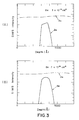
- FIGS.3(A) and (B) show the result of evaluation of the test samples of FIG.2(A) thus formed.
- the compositional profile of Be was measured from the top surface of the GaAlAs layer 35 to the bottom of the GaAlAs layer 33 by secondary ion mass spectroscopy (SIMS), in which FIG.3(A) shows the case in which Be is doped to the layer 34 with a level of 3 X 1019 cm ⁇ 3 and FIG.3(B) shows the case in which Be is doped to the layer 34 with a level of 7 X 1019 cm ⁇ 3.
- the thickness of a region which contains Be is represented as a thickness of a layer containing Be with a concentration level which is one-tenth of the maximum concentration level of Be contained in that region.
- the region of the sample in which Be is contained is confined within a thickness of about 1200 ⁇ in correspondence to the designed layer thickness of the layer 34 when Be is doped within the level of 3 X 1019 cm ⁇ 3. No substantial diffusion of Be beyond the base layer 34 is observed.
- the concentration level of Be is increased to a level of 7 X 1019 cm ⁇ 3
- the thickness of the region in the sample in which Be is contained is broadened to a thickness of about 1500 ⁇ as is clearly seen in FIG.3(B). This means that there is a substantial diffusion of Be from the base layer 34 in agreement with the aforementioned report (Pao, Y.C. et al. op.cit.).
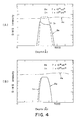
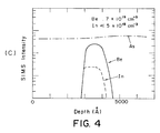
- FIGS.4(A), (B) and (C) show a result of the evaluation for the test sample of FIG.2(B) with a constant doping level of Be at 7 X 1019 cm ⁇ 3 and with various In concentration levels.
- the evaluation was made by SIMS similarly to the foregoing case.
- In is added to Ga 1-x Al x As such that the composition after the addition of In is represented as In y (Ga 1-x Al x ) 1-y As.
- the ratio between Al and Ga is not changed by the addition of In.
- the composition after the addition of In is represented as In y (In x Ga 1-x ) 1-y As.
- the value y is determined by the concentration level of Be to be added for doping as already described. In the case that Be is doped to the level of 5 X 10¹⁹ - 5 X 1020 cm ⁇ 3, a range of y between 0.005 to 0.08 is preferred for eliminating the unwanted abnormal increase of diffusion of Be.
- FIG.5 shows the thickness of the Be-containing region formed in the test sample of FIG.2(B) for various In concentration levels. Similarly to the foregoing experiments, the concentration of Be is fixed at 7 X 1019 cm ⁇ 3. As is clearly seen in this drawing, there is a minimum in the thickness of the Be-containing region in correspondence to the compositional range of about 0.5 mole % to about 8 mole % represented in terms of the InAs component.
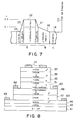
- FIG.6 shows a structure of an HBT according to an embodiment of the present invention.
- an n+-type collector buffer layer of GaAs 13 and an n-type collector 14 of GaAs are grown consecutively on a buffer layer 12 of GaAs which in turn is grown on an (100) surface of a semi-insulating GaAs substrate 11.
- the collector buffer layer 13 has a thickness of 5000 ⁇ and a donor concentration level of 3 X 1018 cm ⁇ 3 while the collector layer 14 has a thickness of 3000 ⁇ and a donor concentration level of 5 X 1016 cm ⁇ 3.
- Be is doped typically to a concentration level of about 1 X 1020 cm ⁇ 3.
- an n-type emitter layer 20 of GaAlAs and an n+-type emitter cap layer 24 are grown epitaxially on the base layer 16 with the compositional gradient of Al as shown in FIG.7.
- the base layer 16 ordinarily achieves the lattice matching with the collector layer 14 when it is free from In and Be.
- Be is doped to a level of 5 X 10¹⁹ - 5 X 1020 cm ⁇ 3 in order to reduce the base spreading resistance, the lattice matching is lost because of the small atomic radius of Be incorporated into the base layer 16.
- the strain induced in the crystal lattice of the p+-type InGaAlAs base layer 16 by the doping of Be is successfully eliminated by the simultaneous addition of In according to the formula In y (Ga 1-x Al x ) 1-y As, in which the parameter y is set to the foregoing range of 0.005 - 0.08 and the foregoing lattice matching is reestablished.
- the composition x for Al is changed with respect to the composition of Ga represented as 1 - x from a value 0.0 at an interface to the collector layer 14 to 0.1 at another interface to the emitter layer 20 independently of the composition y .
- the n-type emitter layer 20 further comprises a first layer 21 having a thickness of about 300 ⁇ and a donor concentration level of about 5 X 1017 cm ⁇ 3 with the aluminium composition ranging from 0.1 to 0.3, a second layer 22 having a thickness of about 900 ⁇ and the same donor concentration level with the aluminium composition of 0.3, and a third layer 23 having a thickness of about 300 ⁇ and the same donor concentration level with the aluminium composition decreasing from 0.3 to zero as illustrated in FIG.7.
- the compositional gradient of Al as such, the band structure across the collector, base and emitter becomes continuous and the undesirable spike and notch in the band structure is eliminated.
- the n+-type cap layer 24 has a thickness of about 1500 ⁇ and a donor concentration level of about 5 X 1018 cm ⁇ 3.
- an emitter electrode 25 is provided on this cap layer 24 .
- a base electrode 26 is provided on the base layer 16 and a collector electrode 27 is provided on the collector buffer layer 13.
- the growth of the layers 12 - 24, particularly the base layer 16, is preferrably made according to the MBE process already described with reference to the formation of the test sample of FIG.2(B) or MOCVD in which a near-ideal stoichiometry is maintained in the group III-V compound semiconductor layers thus grown.
- the epitaxial growth of the layers 16 and 20 containing Al can be made in the temperature rang of 550 - 680 °C, preferably above 600°C.
- the diffusion of Be to the neighbouring emitter layer 20 or collector layer 14 is effectively prevented even the layers 16 and 20 are grown in such a relatively high temperature range and the destruction of the HBT structure is avoided while still maintaining the graded compositional structure which facilitates the high speed operation of the device.
- the HBT is constructed on a semi-insulating InP substrate 41.
- a buffer layer 43 of undoped InAlAs is grown epitaxially on the substrate 41 for a thickness of about 3000 ⁇ while maintaining the lattice matching with the underlying substrate 41, and an n+-type collector contact layer 45 of InGaAs with a donor concentration level of 2 X 1019 cm ⁇ 3 is grown on the buffer layer 43 for a thickness of 5000 ⁇ .
- an n-type collector layer 47 of InGaAs with a donor concentration level of 3 X 1016 cm ⁇ 3 is grown epitaxially on the collector contact layer 45 for a thickness of 5000 ⁇ .
- the composition of the InGaAs layers 45 and 47 is adjusted to In 0.53 Ga 0.47 As and the composition of the InAlAs buffer layer is adjusted to In 0.52 Al 0.48 As in order to achieve the lattice matching with the underlying InP substrate 41.
- a base layer 49 of InGaAlAs is grown epitaxially for a thickness of about 1000 ⁇ .
- the base layer 49 is doped to the p-type by addition of Be to the concentration level of about 1 X 1020 cm ⁇ 3.
- the composition of the base layer 49 is graded such that the concentration of Al is increased gradually from 0 to 0.2 from a bottom boundary of the base layer 49 to a top boundary thereof.
- the concentration of In is increased from 0.53 to a level corresponding to the concentration of Be according to the foregoing relation.
- the Be concentration level is set in the range of 5 X 10¹⁹ - 5 X 1020 cm ⁇ 3
- In is added according to the formula In y [In 0.53 (Ga 1-x Al x ) 0.47 ] 1-y
- the parameter y changes from 0 to 0.2.
- a first emitter layer 51 of InGaAlAs of the n-type and having a composition of In 0.53 (Ga 1-x Al x ) 0.47 As is grown with the parameter x changing from 0.2 to 1 from the bottom to the top, and a second emitter layer 53 of InAlAs doped to the n-type is grown further thereon.
- the first emitter layer 51 has a thickness of about 300 ⁇ and the second emitter layer 53 has a thickness of about 2000 ⁇ .
- the concentration level of the donor is fixed at about 2 X 1017 cm ⁇ 3.
- a first cap layer 55 of InGaAlAs doped to the n-type with the donor concentration level of about 2 X 1019 cm ⁇ 3 is grown on the second emitter layer 53 for a thickness of about 700 ⁇ while changing the composition from one hundred percent InAlAs at the bottom to one hundred percent InGaAs at the top.
- a second cap layer 57 of InGaAs is grown on the first cap layer 55 for a thickness of about 500 ⁇ .
- the second cap layer 57 is doped to a donor concentration level of about 1 X 1019 cm ⁇ 3.
- an emitter electrode 61 of gold-germanium alloy, a base electrode 62 of gold-zinc alloy, and a collector electrode 63 of gold-germanium alloy are provided respectively on the emitter cap layer 57, the base layer 49 and on the collector contact layer 45 and the HBT of this embodiment is completed.
- the growth of the layers 45 through 57 is made by MBE or MOCVD at a temperature of about 600°C or more. Because of the simultaneous doping of Be and In to the base layer 49, the diffusion of Be to the adjacent layers is successfully suppressed in spite of the high temperature employed for the growth of the base layer. Thus, an extremely high speed HBT having the operational speed enhanced by the use of thin but low resistance base layer as well as by the use of the graded compositional profile for the base and the emitter is obtained. Associated with the suppressing of the abnormal diffusion of Be, the reproducibility of the obtained HBT is improved.
Landscapes
- Bipolar Transistors (AREA)
Claims (13)
- Procédé de fabrication d'un dispositif à semiconducteur comprenant une couche épitaxiale (16, 37, 49) faite d'un matériau semiconducteur des groupes III-V qui est disposée sur une couche cristalline sous-jacente (11-14, 31-36, 41-47) en appariement de réseau avec celle-ci, ledit matériau semiconducteur étant dopé suivant le type p par addition de béryllium et étant choisi dans le groupe comprenant l'arséniure de gallium et d'aluminium et l'arséniure d'indium, de gallium et d'aluminium, comprenant l'opération qui consiste à faire croître ladite couche épitaxiale sur la couche cristalline sous-jacente, caractérisé par d'autres opérations, lesquelles consistent à ajouter au matériau semiconducteur du béryllium avec un niveau de concentration d'environ 5 x 10¹⁹ atomes/cm³ à environ 5 x 10²⁰ atomes/cm³, et à ajouter de l'indium dans une proportion d'environ 0,5 mol % à environ 8 mol % par rapport aux éléments du groupe III se trouvant dans ledit matériau semiconducteur.
- Procédé selon la revendication 1, caractérisé en ce que ladite opération d'addition de béryllium et ladite opération d'addition d'indium sont effectuées pendant ladite opération de croissance de la couche épitaxiale (16,37,49).
- Procédé selon la revendication 2, caractérisé en ce que ladite opération d'addition de béryllium et ladite opération d'addition d'indium sont effectuées simultanément.
- Procédé selon la revendication 1, caractérisé en ce que ladite opération de croissance de la couche épitaxiale (16, 37, 49) est faite à une température comprise entre environ 550°C et environ 680°C.
- Procédé selon la revendication 4, caractérisé en ce que ladite opération de croissance de la couche épitaxiale (16, 37, 49) est faite à une température égale ou supérieure à environ 600°C.
- Procédé de fabrication d'un transistor bipolaire, comprenant les opérations consistant à faire croître épitaxialement une couche de collecteur de type n (14, 47) sur une couche cristalline sous-jacente (11-13, 41-45), à faire croître épitaxialement une couche de base (16, 49) d'un matériau semiconducteur composé des groupes III-V choisi dans le groupe de matériaux comprenant l'arséniure de gallium et d'aluminium et l'arséniure d'indium, de gallium et d'aluminium sur la couche de collecteur de type n, caractérisé en ce qu'il comprend les opérations consistant à doper la couche de base suivant le type p par addition de béryllium à la couche de base avec un niveau de concentration d'environ 5 x 10¹⁹ atomes/cm³ à environ 5 x 10²⁰ atomes/cm³, à ajouter de l'indium à la couche de base dans une proportion d'environ 0,5 mol % à environ 8 mol % par rapport aux éléments du groupe III contenus dans la couche de base, et à faire croître une couche d'émetteur de type n (20, 51-55) sur ladite couche de base.
- Procédé selon la revendication 6, caractérisé en ce que ladite opération de dopage et ladite opération d'addition d'indium sont effectuées pendant ladite opération de croissance de la couche de base.
- Procédé selon la revendication 7, caractérisé en ce que ladite opération de dopage et ladite opération d'addition d'indium sont effectuées simultanément.
- Procédé selon la revendication 6, caractérisé en ce que ladite croissance de la couche de base (16, 49) est faite à une température comprise entre environ 550°C et environ 680°C.
- Procédé selon la revendication 6, caractérisé en ce que ladite croissance de la couche de base (16, 49) s'effectue à une température d'environ 600°C ou plus.
- Procédé selon la revendication 6, caractérisé en ce que ladite opération de croissance de la couche de base (16, 49) comprend en outre l'opération consistant à produire une variation graduelle de la teneur en aluminium de la couche de base de façon que la teneur en aluminium augmente continûment, d'un premier côté de la couche de base, en contact avec la couche de collecteur (13, 47), à un deuxième côté de la couche de base, en contact avec la couche d'émetteur (20, 51-55).
- Procédé selon la revendication 6, caractérisé en ce que ladite opération de croissance de la couche d'émetteur comprend en outre l'opération consistant à produire une variation de composition graduelle de la teneur en aluminium de la couche d'émetteur, de façon que la teneur en aluminium augmente continûment, reste constante, puis diminue continûment, d'un premier côté de la couche d'émetteur (20, 51-55), en contact avec la couche de base (16, 49), à un deuxième côté, opposé audit premier côté.
- Procédé de fabrication d'un dispositif à semiconducteur comprenant une couche épitaxiale (16, 37, 49) d'un matériau semiconducteur des groupes III-V disposée sur une couche cristalline sous-jacente (11-14, 31-36, 41-47) en appariement de réseau avec celle-ci, ledit matériau semiconducteur étant dopé suivant le type p par addition de béryllium et étant choisi dans le groupe comprenant l'arséniure de gallium et d'aluminium et l'arséniure d'indium, de gallium et d'aluminium, comprenant l'opération consistant à faire croître ladite couche épitaxiale sur la couche cristalline sous-jacente, caractérisé par les opérations supplémentaires consistant à ajouter du béryllium avec un niveau de concentration prédéterminé, et à ajouter de l'indium dans une proportion généralement égale à celle du béryllium.
Applications Claiming Priority (2)
| Application Number | Priority Date | Filing Date | Title |
|---|---|---|---|
| JP271345/88 | 1988-10-27 | ||
| JP27134588 | 1988-10-27 |
Publications (3)
| Publication Number | Publication Date |
|---|---|
| EP0366552A2 EP0366552A2 (fr) | 1990-05-02 |
| EP0366552A3 EP0366552A3 (en) | 1990-11-28 |
| EP0366552B1 true EP0366552B1 (fr) | 1993-04-28 |
Family
ID=17498768
Family Applications (1)
| Application Number | Title | Priority Date | Filing Date |
|---|---|---|---|
| EP89402953A Expired - Lifetime EP0366552B1 (fr) | 1988-10-27 | 1989-10-25 | Procédé pour fabriquer un transistor bipolaire du type hétérojonction |
Country Status (2)
| Country | Link |
|---|---|
| EP (1) | EP0366552B1 (fr) |
| DE (1) | DE68906239T2 (fr) |
Families Citing this family (3)
| Publication number | Priority date | Publication date | Assignee | Title |
|---|---|---|---|---|
| JPH0669222A (ja) * | 1992-08-17 | 1994-03-11 | Matsushita Electric Ind Co Ltd | ヘテロ接合バイポーラトランジスタ及びその製造方法 |
| US5631477A (en) * | 1995-06-02 | 1997-05-20 | Trw Inc. | Quaternary collector InAlAs-InGaAlAs heterojunction bipolar transistor |
| GB9826519D0 (en) * | 1998-12-02 | 1999-01-27 | Arima Optoelectronics Corp | Semiconductor devices |
-
1989
- 1989-10-25 EP EP89402953A patent/EP0366552B1/fr not_active Expired - Lifetime
- 1989-10-25 DE DE8989402953T patent/DE68906239T2/de not_active Expired - Fee Related
Non-Patent Citations (2)
| Title |
|---|
| Appl. Phys. Lett. 37(1) 1July 1980 p.64-65. * |
| Journal of Crystal Growth 46(1979) 300-303. * |
Also Published As
| Publication number | Publication date |
|---|---|
| DE68906239D1 (de) | 1993-06-03 |
| EP0366552A2 (fr) | 1990-05-02 |
| EP0366552A3 (en) | 1990-11-28 |
| DE68906239T2 (de) | 1993-08-12 |
Similar Documents
| Publication | Publication Date | Title |
|---|---|---|
| US5770868A (en) | GaAs substrate with compositionally graded AlGaAsSb buffer for fabrication of high-indium fets | |
| US5521404A (en) | Group III-V interdiffusion prevented hetero-junction semiconductor device | |
| US5508536A (en) | Heterojunction bipolar transistor having low electron and hole concentrations in the emitter-base junction region | |
| EP0381396A1 (fr) | Dispositifs à semi-conducteur composé | |
| US5952672A (en) | Semiconductor device and method for fabricating the same | |
| EP0740350B1 (fr) | Dispositif semi-conducteur composé à résistance réduite | |
| US5284783A (en) | Method of fabricating a heterojunction bipolar transistor | |
| JP3141838B2 (ja) | 電界効果トランジスタ | |
| EP0366552B1 (fr) | Procédé pour fabriquer un transistor bipolaire du type hétérojonction | |
| JP2620901B2 (ja) | 応力補償層を有するGaAsヘテロ構造 | |
| US7291873B2 (en) | High electron mobility epitaxial substrate | |
| US5814843A (en) | Heterojunction bipolar transistor having a graded-composition base region | |
| US7732836B2 (en) | Compound semiconductor epitaxial substrate and method for manufacturing the same | |
| EP0405832A1 (fr) | Procédés de dopage pour composants semi-conducteurs | |
| Houng | CBE growth of AlGaAs/GaAs heterostructures and their device applications | |
| JP2761264B2 (ja) | 半導体装置の製造方法 | |
| KR100519896B1 (ko) | 고농도로도핑된반도체및그의제조방법 | |
| Ito et al. | Carbon doping in InAlAs grown by metalorganic chemical vapor deposition | |
| JP2980630B2 (ja) | 化合物半導体装置 | |
| Ando et al. | Growth of carbon-doped base GaAs/AlGaAs HBT by gas-source MBE using TEG, TEA, TMG, AsH3, and Si2H6 | |
| Baumann et al. | High temperature MOVPE growth of GaAs/AlGaAs device structures with tertiarybutylarsine | |
| Sandhu et al. | p+/N GaAs-AlGaAs heterostructures grown by gas source MBE using gaseous p-and n-type dopant sources | |
| JPH06267867A (ja) | 化合物半導体の結晶成長法およびこれを用いたオーミックコンタクトの形成法 | |
| EP0430595B1 (fr) | Dispositif semi-conducteur composé | |
| Kobayashi et al. | Growth temperature dependence of Zn diffusion in InPInGaAs heterojunction bipolar transistor structures grown by metalorganic chemical vapor deposition |
Legal Events
| Date | Code | Title | Description |
|---|---|---|---|
| PUAI | Public reference made under article 153(3) epc to a published international application that has entered the european phase |
Free format text: ORIGINAL CODE: 0009012 |
|
| AK | Designated contracting states |
Kind code of ref document: A2 Designated state(s): DE FR GB |
|
| PUAL | Search report despatched |
Free format text: ORIGINAL CODE: 0009013 |
|
| AK | Designated contracting states |
Kind code of ref document: A3 Designated state(s): DE FR GB |
|
| RHK1 | Main classification (correction) |
Ipc: H01L 29/73 |
|
| 17P | Request for examination filed |
Effective date: 19901221 |
|
| 17Q | First examination report despatched |
Effective date: 19920511 |
|
| GRAA | (expected) grant |
Free format text: ORIGINAL CODE: 0009210 |
|
| AK | Designated contracting states |
Kind code of ref document: B1 Designated state(s): DE FR GB |
|
| REF | Corresponds to: |
Ref document number: 68906239 Country of ref document: DE Date of ref document: 19930603 |
|
| ET | Fr: translation filed | ||
| PLBE | No opposition filed within time limit |
Free format text: ORIGINAL CODE: 0009261 |
|
| STAA | Information on the status of an ep patent application or granted ep patent |
Free format text: STATUS: NO OPPOSITION FILED WITHIN TIME LIMIT |
|
| 26N | No opposition filed | ||
| REG | Reference to a national code |
Ref country code: GB Ref legal event code: IF02 |
|
| PGFP | Annual fee paid to national office [announced via postgrant information from national office to epo] |
Ref country code: DE Payment date: 20071018 Year of fee payment: 19 |
|
| PGFP | Annual fee paid to national office [announced via postgrant information from national office to epo] |
Ref country code: GB Payment date: 20071024 Year of fee payment: 19 Ref country code: FR Payment date: 20071009 Year of fee payment: 19 |
|
| GBPC | Gb: european patent ceased through non-payment of renewal fee |
Effective date: 20081025 |
|
| REG | Reference to a national code |
Ref country code: FR Ref legal event code: ST Effective date: 20090630 |
|
| PG25 | Lapsed in a contracting state [announced via postgrant information from national office to epo] |
Ref country code: DE Free format text: LAPSE BECAUSE OF NON-PAYMENT OF DUE FEES Effective date: 20090501 |
|
| PG25 | Lapsed in a contracting state [announced via postgrant information from national office to epo] |
Ref country code: FR Free format text: LAPSE BECAUSE OF NON-PAYMENT OF DUE FEES Effective date: 20081031 |
|
| PG25 | Lapsed in a contracting state [announced via postgrant information from national office to epo] |
Ref country code: GB Free format text: LAPSE BECAUSE OF NON-PAYMENT OF DUE FEES Effective date: 20081025 |