EP0362852A2 - Informationsaufzeichnungsdünnschicht und Methode zur Aufnahme und Wiedergabe von Information - Google Patents
Informationsaufzeichnungsdünnschicht und Methode zur Aufnahme und Wiedergabe von Information Download PDFInfo
- Publication number
- EP0362852A2 EP0362852A2 EP89118519A EP89118519A EP0362852A2 EP 0362852 A2 EP0362852 A2 EP 0362852A2 EP 89118519 A EP89118519 A EP 89118519A EP 89118519 A EP89118519 A EP 89118519A EP 0362852 A2 EP0362852 A2 EP 0362852A2
- Authority
- EP
- European Patent Office
- Prior art keywords
- recording
- thin film
- elements
- film
- information
- Prior art date
- Legal status (The legal status is an assumption and is not a legal conclusion. Google has not performed a legal analysis and makes no representation as to the accuracy of the status listed.)
- Granted
Links
Images


Classifications
-
- G—PHYSICS
- G11—INFORMATION STORAGE
- G11B—INFORMATION STORAGE BASED ON RELATIVE MOVEMENT BETWEEN RECORD CARRIER AND TRANSDUCER
- G11B7/00—Recording or reproducing by optical means, e.g. recording using a thermal beam of optical radiation by modifying optical properties or the physical structure, reproducing using an optical beam at lower power by sensing optical properties; Record carriers therefor
- G11B7/24—Record carriers characterised by shape, structure or physical properties, or by the selection of the material
- G11B7/241—Record carriers characterised by shape, structure or physical properties, or by the selection of the material characterised by the selection of the material
- G11B7/242—Record carriers characterised by shape, structure or physical properties, or by the selection of the material characterised by the selection of the material of recording layers
- G11B7/243—Record carriers characterised by shape, structure or physical properties, or by the selection of the material characterised by the selection of the material of recording layers comprising inorganic materials only, e.g. ablative layers
-
- G—PHYSICS
- G11—INFORMATION STORAGE
- G11B—INFORMATION STORAGE BASED ON RELATIVE MOVEMENT BETWEEN RECORD CARRIER AND TRANSDUCER
- G11B7/00—Recording or reproducing by optical means, e.g. recording using a thermal beam of optical radiation by modifying optical properties or the physical structure, reproducing using an optical beam at lower power by sensing optical properties; Record carriers therefor
- G11B7/004—Recording, reproducing or erasing methods; Read, write or erase circuits therefor
- G11B7/0055—Erasing
- G11B7/00557—Erasing involving phase-change media
-
- G—PHYSICS
- G11—INFORMATION STORAGE
- G11B—INFORMATION STORAGE BASED ON RELATIVE MOVEMENT BETWEEN RECORD CARRIER AND TRANSDUCER
- G11B7/00—Recording or reproducing by optical means, e.g. recording using a thermal beam of optical radiation by modifying optical properties or the physical structure, reproducing using an optical beam at lower power by sensing optical properties; Record carriers therefor
- G11B7/24—Record carriers characterised by shape, structure or physical properties, or by the selection of the material
- G11B7/241—Record carriers characterised by shape, structure or physical properties, or by the selection of the material characterised by the selection of the material
- G11B7/242—Record carriers characterised by shape, structure or physical properties, or by the selection of the material characterised by the selection of the material of recording layers
- G11B7/243—Record carriers characterised by shape, structure or physical properties, or by the selection of the material characterised by the selection of the material of recording layers comprising inorganic materials only, e.g. ablative layers
- G11B2007/24302—Metals or metalloids
- G11B2007/24306—Metals or metalloids transition metal elements of groups 3-10
-
- G—PHYSICS
- G11—INFORMATION STORAGE
- G11B—INFORMATION STORAGE BASED ON RELATIVE MOVEMENT BETWEEN RECORD CARRIER AND TRANSDUCER
- G11B7/00—Recording or reproducing by optical means, e.g. recording using a thermal beam of optical radiation by modifying optical properties or the physical structure, reproducing using an optical beam at lower power by sensing optical properties; Record carriers therefor
- G11B7/24—Record carriers characterised by shape, structure or physical properties, or by the selection of the material
- G11B7/241—Record carriers characterised by shape, structure or physical properties, or by the selection of the material characterised by the selection of the material
- G11B7/242—Record carriers characterised by shape, structure or physical properties, or by the selection of the material characterised by the selection of the material of recording layers
- G11B7/243—Record carriers characterised by shape, structure or physical properties, or by the selection of the material characterised by the selection of the material of recording layers comprising inorganic materials only, e.g. ablative layers
- G11B2007/24302—Metals or metalloids
- G11B2007/24308—Metals or metalloids transition metal elements of group 11 (Cu, Ag, Au)
-
- G—PHYSICS
- G11—INFORMATION STORAGE
- G11B—INFORMATION STORAGE BASED ON RELATIVE MOVEMENT BETWEEN RECORD CARRIER AND TRANSDUCER
- G11B7/00—Recording or reproducing by optical means, e.g. recording using a thermal beam of optical radiation by modifying optical properties or the physical structure, reproducing using an optical beam at lower power by sensing optical properties; Record carriers therefor
- G11B7/24—Record carriers characterised by shape, structure or physical properties, or by the selection of the material
- G11B7/241—Record carriers characterised by shape, structure or physical properties, or by the selection of the material characterised by the selection of the material
- G11B7/242—Record carriers characterised by shape, structure or physical properties, or by the selection of the material characterised by the selection of the material of recording layers
- G11B7/243—Record carriers characterised by shape, structure or physical properties, or by the selection of the material characterised by the selection of the material of recording layers comprising inorganic materials only, e.g. ablative layers
- G11B2007/24302—Metals or metalloids
- G11B2007/2431—Metals or metalloids group 13 elements (B, Al, Ga, In)
-
- G—PHYSICS
- G11—INFORMATION STORAGE
- G11B—INFORMATION STORAGE BASED ON RELATIVE MOVEMENT BETWEEN RECORD CARRIER AND TRANSDUCER
- G11B7/00—Recording or reproducing by optical means, e.g. recording using a thermal beam of optical radiation by modifying optical properties or the physical structure, reproducing using an optical beam at lower power by sensing optical properties; Record carriers therefor
- G11B7/24—Record carriers characterised by shape, structure or physical properties, or by the selection of the material
- G11B7/241—Record carriers characterised by shape, structure or physical properties, or by the selection of the material characterised by the selection of the material
- G11B7/242—Record carriers characterised by shape, structure or physical properties, or by the selection of the material characterised by the selection of the material of recording layers
- G11B7/243—Record carriers characterised by shape, structure or physical properties, or by the selection of the material characterised by the selection of the material of recording layers comprising inorganic materials only, e.g. ablative layers
- G11B2007/24302—Metals or metalloids
- G11B2007/24312—Metals or metalloids group 14 elements (e.g. Si, Ge, Sn)
-
- G—PHYSICS
- G11—INFORMATION STORAGE
- G11B—INFORMATION STORAGE BASED ON RELATIVE MOVEMENT BETWEEN RECORD CARRIER AND TRANSDUCER
- G11B7/00—Recording or reproducing by optical means, e.g. recording using a thermal beam of optical radiation by modifying optical properties or the physical structure, reproducing using an optical beam at lower power by sensing optical properties; Record carriers therefor
- G11B7/24—Record carriers characterised by shape, structure or physical properties, or by the selection of the material
- G11B7/241—Record carriers characterised by shape, structure or physical properties, or by the selection of the material characterised by the selection of the material
- G11B7/242—Record carriers characterised by shape, structure or physical properties, or by the selection of the material characterised by the selection of the material of recording layers
- G11B7/243—Record carriers characterised by shape, structure or physical properties, or by the selection of the material characterised by the selection of the material of recording layers comprising inorganic materials only, e.g. ablative layers
- G11B2007/24302—Metals or metalloids
- G11B2007/24314—Metals or metalloids group 15 elements (e.g. Sb, Bi)
-
- G—PHYSICS
- G11—INFORMATION STORAGE
- G11B—INFORMATION STORAGE BASED ON RELATIVE MOVEMENT BETWEEN RECORD CARRIER AND TRANSDUCER
- G11B7/00—Recording or reproducing by optical means, e.g. recording using a thermal beam of optical radiation by modifying optical properties or the physical structure, reproducing using an optical beam at lower power by sensing optical properties; Record carriers therefor
- G11B7/24—Record carriers characterised by shape, structure or physical properties, or by the selection of the material
- G11B7/241—Record carriers characterised by shape, structure or physical properties, or by the selection of the material characterised by the selection of the material
- G11B7/242—Record carriers characterised by shape, structure or physical properties, or by the selection of the material characterised by the selection of the material of recording layers
- G11B7/243—Record carriers characterised by shape, structure or physical properties, or by the selection of the material characterised by the selection of the material of recording layers comprising inorganic materials only, e.g. ablative layers
- G11B2007/24302—Metals or metalloids
- G11B2007/24316—Metals or metalloids group 16 elements (i.e. chalcogenides, Se, Te)
-
- G—PHYSICS
- G11—INFORMATION STORAGE
- G11B—INFORMATION STORAGE BASED ON RELATIVE MOVEMENT BETWEEN RECORD CARRIER AND TRANSDUCER
- G11B7/00—Recording or reproducing by optical means, e.g. recording using a thermal beam of optical radiation by modifying optical properties or the physical structure, reproducing using an optical beam at lower power by sensing optical properties; Record carriers therefor
- G11B7/24—Record carriers characterised by shape, structure or physical properties, or by the selection of the material
- G11B7/241—Record carriers characterised by shape, structure or physical properties, or by the selection of the material characterised by the selection of the material
- G11B7/242—Record carriers characterised by shape, structure or physical properties, or by the selection of the material characterised by the selection of the material of recording layers
- G11B7/243—Record carriers characterised by shape, structure or physical properties, or by the selection of the material characterised by the selection of the material of recording layers comprising inorganic materials only, e.g. ablative layers
- G11B2007/24318—Non-metallic elements
- G11B2007/24328—Carbon
-
- G—PHYSICS
- G11—INFORMATION STORAGE
- G11B—INFORMATION STORAGE BASED ON RELATIVE MOVEMENT BETWEEN RECORD CARRIER AND TRANSDUCER
- G11B7/00—Recording or reproducing by optical means, e.g. recording using a thermal beam of optical radiation by modifying optical properties or the physical structure, reproducing using an optical beam at lower power by sensing optical properties; Record carriers therefor
- G11B7/24—Record carriers characterised by shape, structure or physical properties, or by the selection of the material
- G11B7/241—Record carriers characterised by shape, structure or physical properties, or by the selection of the material characterised by the selection of the material
- G11B7/252—Record carriers characterised by shape, structure or physical properties, or by the selection of the material characterised by the selection of the material of layers other than recording layers
- G11B7/257—Record carriers characterised by shape, structure or physical properties, or by the selection of the material characterised by the selection of the material of layers other than recording layers of layers having properties involved in recording or reproduction, e.g. optical interference layers or sensitising layers or dielectric layers, which are protecting the recording layers
- G11B2007/25705—Record carriers characterised by shape, structure or physical properties, or by the selection of the material characterised by the selection of the material of layers other than recording layers of layers having properties involved in recording or reproduction, e.g. optical interference layers or sensitising layers or dielectric layers, which are protecting the recording layers consisting essentially of inorganic materials
- G11B2007/2571—Record carriers characterised by shape, structure or physical properties, or by the selection of the material characterised by the selection of the material of layers other than recording layers of layers having properties involved in recording or reproduction, e.g. optical interference layers or sensitising layers or dielectric layers, which are protecting the recording layers consisting essentially of inorganic materials containing group 14 elements except carbon (Si, Ge, Sn, Pb)
-
- G—PHYSICS
- G11—INFORMATION STORAGE
- G11B—INFORMATION STORAGE BASED ON RELATIVE MOVEMENT BETWEEN RECORD CARRIER AND TRANSDUCER
- G11B7/00—Recording or reproducing by optical means, e.g. recording using a thermal beam of optical radiation by modifying optical properties or the physical structure, reproducing using an optical beam at lower power by sensing optical properties; Record carriers therefor
- G11B7/24—Record carriers characterised by shape, structure or physical properties, or by the selection of the material
- G11B7/241—Record carriers characterised by shape, structure or physical properties, or by the selection of the material characterised by the selection of the material
- G11B7/252—Record carriers characterised by shape, structure or physical properties, or by the selection of the material characterised by the selection of the material of layers other than recording layers
- G11B7/257—Record carriers characterised by shape, structure or physical properties, or by the selection of the material characterised by the selection of the material of layers other than recording layers of layers having properties involved in recording or reproduction, e.g. optical interference layers or sensitising layers or dielectric layers, which are protecting the recording layers
- G11B2007/25705—Record carriers characterised by shape, structure or physical properties, or by the selection of the material characterised by the selection of the material of layers other than recording layers of layers having properties involved in recording or reproduction, e.g. optical interference layers or sensitising layers or dielectric layers, which are protecting the recording layers consisting essentially of inorganic materials
- G11B2007/25713—Record carriers characterised by shape, structure or physical properties, or by the selection of the material characterised by the selection of the material of layers other than recording layers of layers having properties involved in recording or reproduction, e.g. optical interference layers or sensitising layers or dielectric layers, which are protecting the recording layers consisting essentially of inorganic materials containing nitrogen
-
- G—PHYSICS
- G11—INFORMATION STORAGE
- G11B—INFORMATION STORAGE BASED ON RELATIVE MOVEMENT BETWEEN RECORD CARRIER AND TRANSDUCER
- G11B7/00—Recording or reproducing by optical means, e.g. recording using a thermal beam of optical radiation by modifying optical properties or the physical structure, reproducing using an optical beam at lower power by sensing optical properties; Record carriers therefor
- G11B7/24—Record carriers characterised by shape, structure or physical properties, or by the selection of the material
- G11B7/241—Record carriers characterised by shape, structure or physical properties, or by the selection of the material characterised by the selection of the material
- G11B7/252—Record carriers characterised by shape, structure or physical properties, or by the selection of the material characterised by the selection of the material of layers other than recording layers
- G11B7/253—Record carriers characterised by shape, structure or physical properties, or by the selection of the material characterised by the selection of the material of layers other than recording layers of substrates
- G11B7/2531—Record carriers characterised by shape, structure or physical properties, or by the selection of the material characterised by the selection of the material of layers other than recording layers of substrates comprising glass
-
- G—PHYSICS
- G11—INFORMATION STORAGE
- G11B—INFORMATION STORAGE BASED ON RELATIVE MOVEMENT BETWEEN RECORD CARRIER AND TRANSDUCER
- G11B7/00—Recording or reproducing by optical means, e.g. recording using a thermal beam of optical radiation by modifying optical properties or the physical structure, reproducing using an optical beam at lower power by sensing optical properties; Record carriers therefor
- G11B7/24—Record carriers characterised by shape, structure or physical properties, or by the selection of the material
- G11B7/241—Record carriers characterised by shape, structure or physical properties, or by the selection of the material characterised by the selection of the material
- G11B7/252—Record carriers characterised by shape, structure or physical properties, or by the selection of the material characterised by the selection of the material of layers other than recording layers
- G11B7/258—Record carriers characterised by shape, structure or physical properties, or by the selection of the material characterised by the selection of the material of layers other than recording layers of reflective layers
- G11B7/2595—Record carriers characterised by shape, structure or physical properties, or by the selection of the material characterised by the selection of the material of layers other than recording layers of reflective layers based on gold
Definitions
- This invention relates to recording of information, particularly to an information-recording thin film capable of recording frequency modulated analog signals such as images, voices, etc. or digital information such as electronic computer data, facsimile signal, digital audio signal, etc. in real time by a recording beam, such as laser beam, electron beam, etc., and to a method for recording and reproducing information by the thin film.
- a recording beam such as laser beam, electron beam, etc.
- 54-41902 discloses various film compositions such as Ge20Tl5Sb5Se70, GE20Bi10Se70,etc., and Japanese Patent Application Kokai (Laid-open) No. 57-24039 discloses films of Sb25Te 12.5 Se 62.5 , Cd14Te14Se72, Bi2Se3, Sb2Se3, In20Te20Se60, Bi25Te 12.5 Se 62.5 , CuSe and Te33Se67.
- An object of the present invention is to provide an infomration-recording thin film with good recording and reproducing characteristics, high sensitivity and high stability, and a method for recording and reproducing information by the thin film.
- the present invention provides an information-recording thin film having an average composition in the film thickness direction of the information-recording thin film represented by the following general formula: Sn x Sb y Te z Se ⁇ A ⁇ B ⁇ C ⁇ wherein X, Y, Z, ⁇ , ⁇ , ⁇ and ⁇ are in ranges of 3 ⁇ x ⁇ 50, 10 ⁇ y ⁇ 70, 10 ⁇ z+ ⁇ ⁇ 87, 0.1 ⁇ z/ ⁇ ⁇ 10, 0 ⁇ ⁇ ⁇ 20, 0 ⁇ ⁇ ⁇ 30 and 0 ⁇ ⁇ ⁇ 30 in atomic percentage.
- A is at least one element of Tl, halogen elements such as I, etc. and alkali metals such as Na, etc., and these elements have such effects to cut the chain-shaped atomic arrangements of Te or Se in materials containing Te or Se or accelerate the crystallization speed, but lower the crystallization temperature and thus the stability of amorphous state will be deteriorated unless a material having a higher crystallization temperature is added thereto.
- B is at least one element of Au, Ag, Cu, Pd, Ta, W, Ir, Sc, Y, Ti, Zr, V, Nb, Cr, Mo, Mn, Fe, Ru, Co, Rh and Ni.
- C is at least one of other elements than Sn, Sb, Te, Se and the elements represented by A and B as defined above as to the first means for attaining the object of the invention and is, for example, at least one of Hg, Al, B, C, Si, N, P, O, lanthanide elements, actinide elements, alkaline earth metal elements, inert gas elements, etc.
- One element or a plurality of elements from those represented by A and B as defined above can be deemed as group C elements, insofar as other elements of the individual groups A and B have been already used.
- Ni can be added to a Sn-Sb-Te-Se-Co system in an amount of less than 30 at.
- the content of Al, Hg, alkaline earth metal elements and inert gas elements be less than 10 at. %.
- composition of the present recording thin film may be changed in the film thickness direction, so far as the average composition in the film thickness direction is kept within the afore-mentioned range, and it is preferable that the composition changes continuously.
- the recording is carried out with an energy beam having such a power for such an irradiation time as to cause a change in the atomic arrangement (change from one phase to another) without any large deformation of the recording thin film.
- the present invention provides an information recording thin film having an average composition in the film thickness direction of the information-recording thin film represented by the following general formula: Sb x Te y A′ z B′ ⁇ C′ ⁇ D ⁇ wherein x y, z, ⁇ , ⁇ and ⁇ are in ranges of 5 ⁇ x ⁇ 70, 10 ⁇ y ⁇ 85, 3 ⁇ z ⁇ 50, 0 ⁇ ⁇ ⁇ 20, 0 ⁇ ⁇ ⁇ 30 and 0 ⁇ ⁇ ⁇ 30.
- A′ is at least one element of Sn, Bi, Pb, Ga, Au and In
- B′ is at least one element of T1, halogen elements such as I, etc., and alkali metals such as Na, etc., and these elements have such effects to cut the chain-shaped atomic arrangements of Te or Se in materials containing Te or Se or accelerate the crystallization speed, but lower the crystallization temperature and thus the stability of amorphous state will be deteriorated unless a material having a higher crystallization temperature is added thereto.
- C′ is at least one element of Ag, Cu, Pd, Ta, W, Ir, Sc, Y, Ti, Zr, V, Nb, Cr, Mo, Mn, Fe, Ru, Co, Rh and Ni
- D is other element than Sb, Te and the elements represented by A′, B′ and C′ as defined above and is, for example, at least one of Hg, Se, S, As, Al, B, C, Si, N, P, O, lanthanide elements, actinide elements, alkaline earth metal elements, inert gas elements, etc.
- Ni can be added to a Sb-Te-Sn-Co system in an amount of less than 30 at.% of Ni and in such a range that the sum total of Ni content and Co content be less than 30 at.% of the upper limit of the content of the group C′ elements.
- the content of Al, Hg, alkaline earth metal elements and inert gas elements be less than 10 at.%.
- the elements of the individual groups used as the first means for attaining the object of the present invention play the following roles.
- Sn, Sb, Te and Se can maintain the amorphous state stably and can perform crystallization fast at the recording and erasing, when contained in appropriate ratios.
- Elements such as Co, etc., represented by B can facilitate absorption of long wavelength light such as semi-conductor laser beam, etc., and can also effectively increase the recording sensitivity and make the crystallization proceed faster.
- Elements such as T1, etc., represented by A can effectively increase the crystallization speed and the stability of amorphous state.
- group A element and the group B element are contained together, high speed crystallization can be attained with a good stability of amorphous state and a high recording sensitivity.
- group A element or group B element When either group A element or group B element is to be contained, it is preferable to add the group A element because of easier formation of the film, but the oxidation resistance is lowered.
- Elements such as Ar, etc., represented by C have no particularly remarkable effect by their addition, and have no large adverse effect so far as added in a small amount.
- the rare earth elements, etc. have a role of increasing the reproduced signal intensity and increasing the crystallization temperature, when contained in an amount of 1 to 20 at.%.
- the present information-recording thin film within the foregoing composition ranges as the first means for attaining the object of the invention has a distinguished recording and reproducing characteristics with a low power laser beam for recording and erasing and also has a good stability.
- ranges for X, Y, Z, ⁇ , ⁇ , ⁇ and ⁇ are as follows: ranges of 5 ⁇ x ⁇ 30, 16 ⁇ y ⁇ 45, 35 ⁇ z+ ⁇ ⁇ 80, 0.2 ⁇ z/ ⁇ ⁇ 5, 0 ⁇ ⁇ ⁇ 15, 0 ⁇ ⁇ ⁇ 20, and 0 ⁇ ⁇ ⁇ 20.
- ranges for X, Y, Z , ⁇ , ⁇ , ⁇ , and ⁇ are as follows: ranges of 7 ⁇ x ⁇ 23, 22 ⁇ y ⁇ 40, 40 ⁇ z+ ⁇ ⁇ 70, 0.25 ⁇ z/ ⁇ ⁇ 4, 0 ⁇ ⁇ ⁇ 10, 0 ⁇ ⁇ ⁇ 10, and 0 ⁇ ⁇ ⁇ 10.
- the film is easy to make when ⁇ ⁇ 0.
- a range of 1 ⁇ ⁇ + ⁇ ⁇ 15 more complete erasing can be assured and the time for maintaining the recording can be prolonged.
- Tl is particularly preferable, I is next preferable, and then other halogen elements such as Cl, etc. are preferable.
- rare earth elements are preferable.
- Sb, Se and S it is preferable that the contents of Sb, Se and S are increased in the neighborhood of one of the boundaries of a recording thin film (including a boundary to other layer), as compared with those at the inside, and the oxidation resistance can be increased thereby.
- Sb, Te and elements such as Sn, etc., represented by A′ can maintain the amorphous state stably and can perform crystallization fast at the recording and erasing, when contained in appropriate ratios.
- Elements such as Co, etc. represented by C′ can facilitate absorption of long wavelength light such as semi-conductor laser beam, etc., and can also effectively increase the recording sensitivity and make the crystallization proceed faster.
- Elements such as Tl, etc. can effectively increase the crystallization speed and the stability of amorphous state.
- group B′ element and the group C′ element are contained together, high speed crystallization can be attained with a good stability of amorphous state and a high recording sensitivity.
- group B′ element or group C′ element When either group B′ element or group C′ element is to be contained, it is preferable to add the group B′ element because of easier formation of the film, but the oxidation resistance is lowered.
- Elements such as Ar, etc., represented by D have no particularly remarkable effect by their addition, and have no large adverse effect so far as added in a small amount.
- the rare earth elements, etc. have a role of increasing the reproduced signal intensity and increasing the crystallization temperature, when contained in an amount of 1 to 20 at.%.
- addition of 1 to 20 at.% of Se and S is effective for increasing the oxidation resistance so far as other elements are kept in constant ratios, but the heat resistance is a little lowered.
- An Se content of 1 to 3 at.% is preferable also for the erasing characteristics.
- More preferable ranges for x, y, z, ⁇ , ⁇ , and ⁇ as the second means for attaining the object of the present invention are as follows: ranges of 10 ⁇ x ⁇ 45, 35 ⁇ y ⁇ 80, 5 ⁇ z ⁇ 30, 0 ⁇ ⁇ ⁇ 15, 0 ⁇ ⁇ ⁇ 20, and 0 ⁇ ⁇ ⁇ 10.
- the recording sensitivity is lowered, so long as the Te content is lower, and a range of 60 ⁇ y ⁇ 70 is particularly preferable.
- the film is easy to make when ⁇ ⁇ 0.
- a range of 1 ⁇ ⁇ + ⁇ ⁇ 20 more complete erasing can be assured and the time for maintaining the recording can be prolonged.
- ranges of 1 ⁇ ⁇ ⁇ 10 and 1 ⁇ ⁇ ⁇ 10 the degree of signal modulation can be increased.
- the elements represented by B′ Tl is particularly preferable, I is next preferable and then other halogen atoms such as Cl, etc. are preferable.
- the elements represented by D the rare earth elements are preferable.
- the elements represented by A′, Pb, Ga and In lower the oxidation resistance a little, but In has distinguished recording and erasing characteristics. Au lowers the recording sensitivity, but can increase the oxidation resistance.
- the protective layer may be composed of a organic material such as acrylic resin, polycarbonate, polyolefin, epoxy resin, polyimides, polyamides, polystyrene, polyethylene, polyethylene terephthalate, fluorocarbon resin such as polytetrafluoroethylene (Teflon), etc., which can serve as a substrate, or may be composed of inorganic materials containing oxides, fluorides, nitrides, sulfides, carbides, borides, boron, carbon or metals as the main component, or may be composed of their composite materials.
- a substrate composed of glass, quartz, sapphire, iron, titanium, or aluminum as the main component can work as the inorganic protective layer on one side.
- the organic and inorganic materials tight covering with the inorganic materials is preferivelyable with respect to the heat resistance.
- a thicker inorganic material layer (excluding the application as a substrate) is liable to cause at least one of crack development, decrease in transmissivity, and decrease in sensitivity, and thus the inorganic material layer must be made thinner, and it is preferable to tightly cover the opposite side of the inorganic material layer to the recording film side with a thicker organic material layer to increase the mechanical strength.
- the organic material layer may be a substrate. Deformation can be made less thereby.
- the organic materials for use to this end include, for example, polystyrene, polytetrafluoroethylene (Teflon), polyimides, acrylic resin, polycarbonate, epoxy resin, ethylene-vinyl acetate copolymer, etc. known as hot-melt adhesives, and tackifying agents, etc. UV light curing resin may be used.
- a protective layer composed of inorganic materials can be formed as such by electron beam deposition, sputtering, etc. or can be more readily formed by reactive sputtering, or by forming a film composed of at least one element of metals, semi-metals and semiconductors, and reacting the film with at least one of oxygen, sulfur and nitrogen.
- Inorganic material protective layers are composed of, for example, oxides of at least one element selected from the group consisting of Ce, La, Si, In, Al, Ge, Pb, Sn, Bi, Te, Ta, Sc, Y, Ti, Zr, V, Nb, Cr, and W, sulfides or selenides of at least one element selected from the group consisting of Cd, Zn, Ga, In, Sb, Ge, Sn, and Pb, fluorides of Mg, Ce, Ca, etc., nitrides of Si, Al, Ta, B, etc., and boron and carbon, and the main component has a composition approximating to one of, for example, CeO2, La2O3, SiO, SiO2, In2O3, Al2O3, GeO, GeO2, PbO, SnO, SnO2, Bi2O3, TeO2, WO2, WO3, Ta2O5, Sc2O3, Y2O3, TiO2, ZrO2, CdS, ZnS, CdS
- sulfides approximating to ZnS are preferable with respect to an appropriately large refractive index and a high stability of the film.
- nitrides have not so high surface reflectivity and can produce a stable film, and a composition approximating to TaN, Si3N4 or AlN (aluminum nitride) is preferable with respect to rigidity.
- Preferable oxides have a composition approximating to Y2O3, Sc2O3, CeO2, TiO2, ZrO2, SiO, Ta2O5, In2O3, Al2O3, SnO2 or SiO2.
- Amorphous materials of Si containing hydrogen are also preferable.
- crystallization is carried out by exposure to a laser beam, or an electron beam condensed to a spot diameter of 2 ⁇ m or less, exposure to UV light from a xenon lamp, a mercury lamp, etc. together with heating, exposure to light from a flash lamp, exposure to a large light spot from a high power gas laser, or a combination of exposure to laser beam and heating, etc.
- Crystallization may be carried out only on the recording track, while keeping the intertrack spaces in an amorphous state. Crystallization can be also carried out only on the intertrack spaces.
- Sn, Sb, Te and Se are often not substantially in a combined state right after the vapor deposition.
- the atomic arrangement is in a highly random state.
- the recording track is exposed to a laser beam of high power density to melt the film, if necessary.
- the recording is carried out by formation of amorphous state, and when te recording track is further exposed to a laser beam of low power density to effect crystallization, the reflectivity is liable to become uniform along the entire track. It is also possible to record on a recording thin film in an amorphous state by crystallization. It is also possible to conduct the recording with a power-modulated laser beam between the crystallization power level and the amorphous state-formation power level.
- the reflected light When a thin film is exposed to light, the reflected light is generally a superposition of a reflected light from the thin film surface and another reflected light from the back side of the thin film, and thus undergoes an interference.
- the effect of interference When a signal is read through changes in the reflectivity, the effect of interference is increased by providing a reflecting (absorbing) layer near the recording film, and consequently the read-out signal can be intensified.
- it is preferable to provide an intermediate layer between the recording film and the reflecting (absorbing) layer.
- the intermediate layer is also effective for preventing mutual diffusion between the recording film and the reflecting layer at the recording and rewriting.
- the intermediate layer can perform at least some of recording by selecting the materials of the intermediate layer, for example, by making the intermediate layer of selenide, that is, by diffusing at least some of elements of the recording film into the intermediate layer or diffusing at least some of elements of the intermediate layer into the recording film or the reflecting layer.
- the intermediate layer has a thickness of 3 nm to 600 nm, selected so that the reflectivity of the recording member can become a minimum at the wavelength of read-out light in a recorded or erased state.
- the reflecting layer can be formed between the recording film and the substrate, or on the opposite sides of the recording film.
- Particularly preferable thickness of the intermediate layer for the first means for attaining the object of the present invention is in ranges of 5 nm to 130 nm, 180 nm to 230 nm, 280 nm to 330 nm and 380 nm to 430 nm.
- particularly preferable thickness of the intermediate layer is in range of 60/N nm to 160/N nm and 470/N nm to 570/N nm, where N is the refractive index of the intermediate layer. It is also preferable to form a protective layer composed of the above-mentioned inorganic material on the opposite side of the reflecting layer to the intermediate layer. These three layers (the intermediate layer, the reflecting layer and the protective layer) provide a stronger protective layer on the whole than a single protective layer.
- Metals, semi-metals and semi-conductors can be used for the reflecting layer, but it is preferable to make the reflecting layer from a layer of single substance such as Au, Ag, Cu, Al, Ni, Fe, Co, Cr, Ti, Pd, Pt, W, Ta or Mo, or an alloy or a plurality of alloy of some of these elements as the main components, or a composite layer of these elements with other substances such as an oxygen in an oxide form, etc.
- the reflecting layer is capable of increasing the thermal conductivity and effectively ensures the formation of amorphous state when exposed to a laser beam of high power, even if a recording film capable of undergoing high speed crystallization is used.
- the intermediate layer it is also particularly preferable to make the intermediate layer from a material having a composition approximating to Al2O3, AlN, Si3N4, ZnS, etc. having a higher thermal conductivity or a material having an intermediate thermal conductivity (0.02 W/cm ⁇ deg to 0.1 W/cm ⁇ deg) such as SiO2, etc. to make the intermediate layer thinner.
- the present recording film can be in a dispersion in the oxides, fluorides, nitrides, organic materials, etc., or carbon or carbides to be applicable as a protective layer, as mentioned above, by co-vapor deposition or co-sputtering, whereby in some cases the light absorption coefficient can be adjusted or the reproduced signal intensity can be increased.
- Preferable mixing ratio is such that a proportion of oxygen, fluorine, nitrogen, and carbon in the entire film be 40 at.% or less.
- Preferable ranges for the thickness of the individual members are as follows: Recording film without a reflecting layer: 15 nm to 500 nm, particularly preferably 25 nm to 300 nm with respect to the reproduced signal intensity and recording sensitivity; Recording film with a reflecting layer: 15 nm to 150 nm, particularly preferably 20 nm to 60 nm; Protective layer of inorganic material: 5 nm to 500 nm; in the case of protection by a substrate of inorganic material itself, 0.1 to 20 nm; Protective layer of organic material: 10 nm to 10 mm, or 500 nm to 10 mm; Intermediate layer: 3 to 600 nm; it is preferable that the intermediate layer is thinner than the protective layer; most preferably 20 nm to 90 nm; Light-reflecting layer: 5 to 300 nm; Protective layer of inorganic material adjacent to the light-reflecting layer: 50 nm to 500 nm;
- the afore-mentioned materials and layer thickness of the respective layers other than the recording film are effective not only for the present recording film, but also for other phase change-type recording films, magneto-optical recording films, mutual diffusion-type recording films, etc.
- the foregoing individual layers can be formed by vacuum evaporation, evaporation in a gas, sputtering, ion beam deposition, ion plating, electron beam deposition, casting, spin coating, plasma polymerization, etc. upon proper selection. It is most preferable to form all of the protective layer, the recording film, the intermediate layer, the reflecting layer and the protective layer adjacent to the reflecting layer by sputtering.
- the amorphous state In the present recording film, it is not always necessary to utilize a change between the amorphous state and the crystalline state in recording, but a change in the optical properties must be made by some change in the atomic arrangement without any substantial change in the form of the film. For example, it may be a change in the crystal grain size or crystal form, or a change between the crystalline state and the meta-stable state ( ⁇ , ⁇ , etc.). Even in the change between the amorphous state and the crystalline state, the amorphous state may not be a complete amorphous state, but can contain part of the crystalline state.
- Recording can be carried out by migration of some of atoms constituting the recording film, protective layer and intermediate layer between the recording film and at least one of the protective layer and the intermediate layer by diffusion, chemical reaction, etc. or by both migration and phase change.
- the present recording member can be used not only in a disk form, but also in a tape form, a card form or in any other form.
- Se-based materials In an optical recording medium capable of recording and reproduction by a light beam, Se-based materials have distinguished oxidation resistance, but have no satisfactory recording sensitivity and Te-based materials have a good recording sensitivity, but have no satisfactory oxidation resistance.
- Sn-Sb-Te-Se-based materials can maintain both properties at high levels in the medium and thus can provide a distinguished phase change-type recording medium.
- a UV light curing resin replica layer of tracking grooves serving also as a protective layer was formed on the surface of a disk form, chemically reinforced glass plate.
- the glass disk was 13 cm in diameter and 1.2 mm thick, and one track was divided into 32 sectors, and track addresses and sector addresses were formed in the form of concave and convex pits at the individual intermediate summit parts between the grooves at the starting points of the individual sectors (these parts will be hereinafter referred to as "headers").
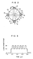
- headers At first a Si3N4 layer, about 300 nm thick, as a protective layer was formed on a substrate 14 by magnetron sputtering. Then, the substrate was disposed in a vacuum evaporation apparatus having an internal structure as shown in Fig.
- evaporation sources 1 , 2 , 3 and 4 were provided in the evaporation apparatus.
- Three of the evaporation sources were evaporation boats by resistance heating and one thereof was an electron beam evaporation source. These boats and electron beam evaporation source were provided under parts on the substrate 14 destined to record information and substantially on a circumference concentric with the center axis of rotation of the substrate. Sb, Te and Se were placed in the three evaporation boats, respectively, and Sn was placed in the electron beam evaporation source. Between the individual boats and the substrate there were provided masks 6 , 7 , 8 and 9 having a sector slit and shutters 10 , 11 , 12 and 13 . The substrate 14 was set to rotate at 120 rpm, while an electric current was passed to the individual boats and the electron beam evaporation source was irradiated with an electron beam to evaporate the source materials.
- the evaporating rates from the individual evaporation sources were detected by quartz-crystal type film thickness monitors 15 , 16 , 17 and 18 to control the electric current thereby to make the evaporation rates constant.
- a recording film 21 having the composition of Sn14Sb30Te28Se28 was vapor deposited to a film thickness of about 30 nm on the Si3N4 layer 20 on the substrate 19 .
- an intermediate layer 22 having a composition substantially equal to Si3N4 was successively formed to a film thickness of about 80 nm thereon also by magnetron sputtering.
- a reflecting layer 23 of Au was formed to a film thickness of about 50 nm thereon by magnetron sputtering.
- a protective layer 20 ′ having a composition substantially equal to Si3N4 on another similar substrate 19′, and a recording film 21 ′ having the composition of Sn14Sb30Te28Se28, an intermediate layer 22 ′ having a composition substantially equal to Si3N4 and a reflecting layer 23 ′ of Au were successively formed thereon.
- Si3N4 protective layers 24 and 24 ′ were formed each to a film thickness of about 200 nm on the vapor-deposited layers 23 and 23 ′ of the thus obtained two substrates 19 and 19 ′, respectively, and the thus obtained two substrates 19 and 19 ′ were joined together by pasting through an organic adhesive layer 25 so that the layers 24 and 24 ′ could be faced inwardly. In this manner, a disk could be prepared.
- the thus prepared disk was subjected to recording, reproduction and erasing in the following manner:
- the disk was rotated at 1,800 rpm, and one of the recording films was exposed to a beam of argon ion laser (wavelength: 830 nm), kept at a non-recording level and condensed by a lens in the recording head, through the substrate.
- the reflected light was detected to drive the head so that the center of the light spot could always fall onto the intermediate part between the tracking grooves.
- the influence of noises generated from the grooves could be prevented by making the intermediate part between the grooves a recording track.
- Automatic focussing was carried out so that the focus could fall on the recording film while conducting the tracking in this manner.
- the recording film on the recording tracks was heated by continuous irradiation of a laser beam of high power density to subject the individual elements to reaction and crystallization.
- An appropriate laser power range for the formation of an amorphous state was higher than the power for the crystallization and lower than the power capable of causing a remarkable transformation or making holes.
- An appropriate laser power range for the crystallization was high enough to cause the crystallization and lower than the power for causing formation of an amorphous state.
- the disk was rotated at 1,800 rpm, and one of the recording films was exposed to a beam of semi-conductor laser (wavelength: 830 nm), kept at a non-recording power level (about 1 mW) and condensed by a lens in the recording head, through the substrate.
- the reflected light was detected to drive the head so that the center of the light spot could always fall onto the intermediate part between the tracking grooves, whereby the influence of noises generated from the grooves could be prevented.
- Automatic focusing was carried out so that the focus could fall on the recording film while conducting the tracking in this manner, and in the recording part recording was carried out by changing a laser power between an intermediate power level of 10 mW and a high power level of 18 mW, as shown in Fig.
- a power ratio of the high power level to the intermediate power level was particularly preferably in a range of 1:0.4 to 1:0.6. Other power levels could be used at short intervals.
- the amorphous portion in the recorded part was regarded as a recording point. After the recording part, the laser power was lowered to 1 mW, and the tracking and automatic focusing were continued. During the recording, the tracking and autofocussing were continued. When such recording procedure was applied to the already recorded part, the recorded information was replaced with newly recorded information. That is, it was possible to make overwriting by a single circular light spot. It is the feature of the present recording film materials as disclosed in this Example that such overwriting is possible in this manner.
- Recording and erasing could be carried out in repetitions of at least 100. Without the Si3N4 layers over and below recording films, the noise was slightly increased after a few repetitions of recording and erasing.
- the disk was rotated at 1,800 rpm, and the intensity of reflected light of semi-conductor laser beam with such a low power not enough to effect recording and erasing was detected to reproduce information, while conducting the tracking and autofocussing in the same manner as in the recording.
- reproduced signal voltage of about 100 mV was obtained.
- the recording film according to this Example had a good oxidation resistance.
- the recording film without formation of the Si3N4 protective layer was not substantially oxidized even if placed at 60°C and a relative humidity of 95%.
- the necessary laser beam power and degree of signal modulation for the recording were changed as follows, when a ratio of Te to Se was changed while keeping the Se content, Sb content and the sum total of Te and Se contents constant.
- the Se content was increased, the thickness of the recording film was made a little larger.
- Degree of signal modulation Sn14Sb30Te4Se52 25% Sn14Sb30Te 5.1 Se 50.9 25% Sn14Sb30Te 9.4 Se 46.6 20% Sn14Sb30Te 11.2 Se 44.8 20% Sn14Sb30Te 44.8 Se 11.2 20% Sn14Sb30Te 46.6 Se 9.4 15% Sn14Sb30Te 50.9 Se 5.1 10% Sn14Sb30Te52Se4 5%
- the necessary irradiation time for erasing was changed as follows, when the Sb content was changed, while keeping the ratio of other elements constant. Necessary irradiation time for erasing Sn19Sb5Te38Se38 5.0 ⁇ s Sn18Sb10Te36Se36 1.0 ⁇ s Sn18Sb12Te35Se35 0.5 ⁇ s Sn17Sb14Te 34.5 Se 34.5 0.1 ⁇ s Sn12Sb40Te24Se24 0.1 ⁇ s Sn11Sb45Te22Se22 0.5 ⁇ s Sn6Sb70Te12Se12 1.0 ⁇ s Sn5Sb75Te10Se10 5.0 ⁇ s
- the necessary laser beam power for recording and the necessary irradiation time for erasing were changed as follows, when the Sn content was changed while keeping the ratio of other elements constant. Necessary laser power for recording Sn2Sb34Te32Se32 16 mW Sn3Sb34Te 31.5 Se 31.5 16 mW Sn5Sb33Te31Se31 16 mW Sn7Sb32Te 30.5 Se 30.5 16 mW Sn23Sb27Te25Se25 16 mW Sn30Sb24Te23Se23 18 mW Sn50Sb 17.4 Te 16.3 Se 16.3 20 mW Sn54Sb16Te15Se15 not recorded Necessary irradiation time for erasing Sn2Sb34Te32Se32 2.0 ⁇ s Sn3Sb34Te 31.5 Se 31.5 1.0 ⁇ s Sn5Sb33Te31Se31 0.5 ⁇ s Sn7Sb32Te 3
- the necessary irradiation time for erasing and the crystallization temperature when heated at a constant rate were changed as follows, when the composition was changed by adding Sn(Te 0.5 Se 0.5 ) to Sb2(Te 0.5 Se 0.5 )3.
- Crystallization temperature when heated at a constant rate and the necessary laser power for recording were changed as follows, when the Co content was changed, while keeping the ratio of other elements constant.
- a film thickness of the intermediate layer of 20 nm to 90 nm was most preferable with respect to a large erasing ratio.
- the smaller the film thickness the higher the cooling rate after the irradiation of laser beam, and the more secure the formation of an amorphous state.
- At least one of halogen elements and alkali metal elements could be added in place of a portion or all of Tl, whereby quite similar characteristics can be obtained.
- halogen atoms of F, Cl, Br and I I was particularly preferable and Cl was next preferivelyable.
- alkali metal elements of Li, Na, K, Rb and Cs Na was particularly preferable and K was next preferable.
- At least one of Au, Ag, Cu, Sc, Y, Zr, V, Nb, Cr, Mo, Mn, Fe, Ru, Ti, Rh, Ta, W, Ir and Ni could be added in place of a portion or all of Co, whereby quite similar characteristics could be obtained.
- at least one of Ti, V, Cr, Mn, Zr and Ni was preferable with respect of easy vapor deposition.
- oxides such as SiO2, SiO, Al2O3, Y2O3, etc., nitrides such as TaN, AlN, etc., sulfides such as ZnS, Sb2S3, etc., fluorides such as CeF3, etc., and compositions similar to amorphous Si, TiB2, C, B4C, BC, etc. could be also used.
- An as a reflecting layer Ag, Cu, Al, Ni, Fe, Co, Cr, Ti, Pd, Pt, W, Ta, Mo, etc. could be used, whereby similar characteristics could be obtained.
- a UV light curing resin replica layer of tracking grooves also serving as a protective layer was formed on the surface of a disk form, chemically reinforced glass plate.
- the glass disk was 13 cm in diameter and 1.2 mm thick, one track was divided into 32 sectors, and track addresses and sector addresses were formed in the form of concave and convex pits at the individual intermediate summit parts between the grooves at the starting points of the individual sectors (these parts will be hereinafter referred to as "headers").
- headers At first a SiO2 layer 20 , about 300 nm thick as a protective layer was formed on a substrate 19 by magnetron sputtering.
- the SiO2 layer may have some unevenness or fluctuation in the film thickness, because the SiO2 layer has only a small difference in the refractive index from the substrate.
- the substrate was disposed in a sputtering apparatus capable of successivelysively forming lamination layers with a uniform film thickness and a good reproducibility, the apparatus having a plurality of targets, and ZnS was formed thereon to a film thickness of about 110 nm as a layer 21 by sputtering and then a recording film 22 having a composition of Sn 14.3 Sb 28.6 Te 57.1 was formed on the ZnS layer 21 to a film thickness of 30 nm in the same sputtering apparatus.
- a protective layer 23 of ZnS was formed thereon to a film thickness of about 50 nm in the same sputtering apparatus.
- a reflecting layer 24 of Au was formed thereon to a film thickness of about 50 nm and then a protective layer of ZnS 25 thereon to a film thickness of 150 nm in the same sputtering apparatus.
- a SiO2 layer 20 ′, a ZnS layer 21 ′, a recording film 22 ′ having a composition of Sn 14.3 Sb 28.6 Te 57.1 , a ZnS layer 23 ′, an Au reflecting layer 24 ′ and a ZnS layer 25 ′ were successively formed on another similar substrate 19 ′.
- the thus prepared disk was subjected to recording, reproduction and erasing in the following manner.
- the disk was rotated at 1,800 rpm, and one of the recording films was exposed to a beam of semi-conductor laser (wavelength: 830 nm), kept at a non-recording power level and condensed by a lens in the recording head, through the substrate.
- the reflected light was detected to drive the head so that the center of the light spot could always fall onto the intermediate part between the adjacent tracking grooves.
- the intermediate part between the adjacent tracking grooves as a recording track, the influence of noises generated from the grooves could be prevented.
- Automatic focusing was carried out so that the focus could fall on the recording film while conducting the tracking in this manner.
- the recording film on the recording track was heated by continuous irradiation of a laser beam of high power density to subject the individual elements to reaction and crystallization.
- An appropriate laser power range for the formation of an amorphous state was higher than the power for the crystallization and lower than the power capable of causing a remarkable transformation or making holes.
- An appropriate laser power range for the crystallization was high enough to cause the crystallization and lower than the power for causing formation of an amorphous state.
- the disk was rotated at 1,800 rpm, and one of the recording films was exposed to a beam of semi-conductor laser (wavelength: 830 nm), kept at a non-recording power level (about 1mW) and condensed by a lens in the recording head, through the substrate.
- the reflected light was detected to drive the head so that the center of the light spot could always fall onto the intermediate part between the tracking grooves, whereby the influence of noises generated from the grooves could be prevented.
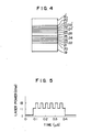
- Automatic focusing was carried out so that the focus could fall ont he recoridng film while conducting the tracking in this matter, and in the recording part recording was carried out by changing a laser power between an intermediate power level of 11 mW and a high power level of 18 mW, as shown in Fig. 5.
- a power ratio of the high power level to the intermediate power level is particularly preferably in a range of 1:0.4 to 1:0.8. Other power levels can be used at short intervals.
- the amorphous portion in the recorded part was regarded as a recording point. After the recording part, the laser power was lowered to 1 mW, and the tracking and automatic focusing were continued. During the recording, the tracking and autofocussing were continued.
- Recording and erasing could be carried out in repetitions of at least 105. Without the ZnS layers over and below recording films, the noise was slightly increased after a few repetitions of recording and erasing.
- the disk was rotated at 1,800 rpm, and the intensity of reflected light of semi-conductor laser beam with such a lower power not enough to effect recording and erasing was detected to reproduce information, while conducting the tracking and auto-focussing in the same manner as in the recording.
- reproduced signal voltage of about 100 mV was obtained.
- the recording film according to this Example had a good oxidation resistance.
- the recording film without formation of the ZnS protective layer was not substantially oxidized even if placed at 60°C and a relative humidity of 95%.
- the necessary irradiation time for erasing was changed as follows, when the Sb content was changed, while keeping a ratio of other elements constant. Necessary irradiation time for erasing Sn 19.4 Sb3Te 77.6 5.0 ⁇ s Sn19Sb5Te76 1.0 ⁇ s Sn18Sb10Te72 0.5 ⁇ s Sn 17.4 Sb13Te 69.6 0.1 ⁇ s Sn12Sb40Te48 0.1 ⁇ s Sn11Sb45Te44 0.5 ⁇ s Sn6Sb70Te24 1.0 ⁇ s Sn5Sb75Te20 5.0 ⁇ s
- the necessary irradiation time for erasing was changed as follows, when the Tl content was changed, while keeping the ratio of other elements constant.
- Crystallization temperature when heated at a constant rate and the necessary laser beam power for recording were changed as follows, when the Co content was changed, while keeping the ratio of other elements constant.
- At least one of Br, Pb, Ga, Au and In could be added in place of a portion or all of Sn, whereby similar characteristics could be obtained.
- halogens and alkali metals When at least one element of halogens and alkali metals was added in place of a portion or all or Tl, quite similar characteristics were obtained.
- I was particularly preferable among the halogens F, C, Br and I, and Cl is next preferable.
- Na was particularly preferable among the alkali metals Li, Na, K, Rb and Cs, and K was next preferable.
- At least one of Cu, Ag, Sc, Y, Zr, V, Nb, Cr, Mo, Mn, Fe, Ru, Ti, Rh, Ta, W, Ir, and Ni could be added in place of a portion or all of Co, whereby quite similar characteristics could be obtained.
- At least one of Ti, V, Cr, Mn, Zr and Ni was preferable among them, because of easy vapor deposition.
- oxides such as SiO2, SiO, Y2O3, nitrides such as TaN, AlN, Si3N4, etc., sulfides such as Sb2S3, etc., selenides such as SnSe2, SbSe2, etc., fluorides such as CeF3, etc. or amorphous materials of Si, TiB2, B4C, BC, etc. or materials having a composition approximating to any of the foregoing materials could be used.
- Lamination film of these materials double or more than double layer was effective for an increase in the protective strength.
- a double layer structure of a 300 nm-thick SiO2 layer provided on the or side from the recording film and a 110 nm-thick ZnS layer provides on the near side from the recording film had less change in the characteristics by rewriting and was found better.
- Ag, Cu, Ni, Fe, Al, Co, Cr, Ti, Pd, Pt, W, Ta, Mo, etc. could be used in place of a portion or all of Au, whereby similar characteristics could be obtained.
- a substrate As a substrate, a polycarbonate plate, a polyolefin plate, an epoxy resin plate, an acrylic resin plate, etc. with concave and convex parts such as tracking guides, directly provided on the surface, could be used in place of the chemically reinforced glass plate with a UV curing resin layer formed on the surface.
- a UV light curing resin replica layer of tracking grooves serving also as a protective layer was formed on the surface of a disk form, chemically reinforced glass plate.
- the glass disk was 13 cm in diameter and 1.2 mm thick, and one track was divided into 32 sectors, and track addresses and sector addresses were formed in the form of concave and convex pits at the individual intermediate summit parts between the grooves at the starting points of the individual sectors (these parts will be hereinafter referred to as "headers").
- headers At first a Si3N4 layer, about 300 nm thick, as a protective layer was formed on a substrate 14 by magnetron sputtering. Then, the substrate was disposed in a vacuum evaporation apparatus having an internal structure as shown in Fig.
- evaporation sources 1 , 2 , 3 and 4 were provided in the evaporation apparatus.
- Three of the evaporation sources were evaporation boats by resistance heating and one thereof was an electron beam evaporation source. These boats and electron beam evaporation source were provided under parts on the substrate 14 destined to record information and substantially on a circumference concentric with the center axis of rotation of the substrate. Sn, Sb and Te were placed in the three evaporation boats, respectively, and Te was placed in the electron beam evaporation source.
- masks 6 , 7 , 8 and 9 having a sector slit and shutters 10 , 11 , 12 and 13 .
- the substrate 14 was set to rotate at 120 rpm, while an electric current was passed to the individual boats and the electron beam evaporation source was irradiated with an electron beam to evaporate the source materials.
- the evaporating rates from the individual evaporation sources were detected by quartz-crystal type film thickness monitors 15 , 16 , 17 and 18 to control the electric current thereby to make the evaporation rates constant.
- a recording film 21 having the composition of Sn15Sb30Te55 was vapor deposited to a film thickness of about 80 nm on the Si3N4 layer 20 on the substrate 19 .
- a protective layer 22 having a composition substantially equal to Si3N4 was successively formed to a film thickness of about 100 nm thereon also by magnetron sputtering.
- a reflecting layer 23 of Au was formed to a film thickness of about 50 nm thereon by electron beam vapor deposition.
- a protective layer 20 ′ having a composition substantially equal to Si3N4 on another similar substrate 19 ′, and a recording film 21 ′ having the composition of Sn15Sb30Te55, a protective layer 22 ′ having a composition substantially equal to Si3N4 and a reflecting layer 23 ′ of Au were successively formed thereon.
- Si3N4 protective layers 24 and 24 ′ were formed each to a film thickness of about 200 nm on the vapor-deposited layers 23 and 23 ′ of the thus obtained two substrates 19 and 19 ′, respectively, and the thus obtained two substrates 19 and 19 ′ were joined together by pasting through an organic adhesive layer 25 so that the layers 24 and 24 ′ could be faced inwardly. In this manner, a disk could be prepared.
- the thus prepared disk was subjected to recording, reproduction and erasing in the following manner:
- the disk was rotated at 1,800 rpm, and one of the recording films was exposed to a beam of argon ion laser (wavelength: 830 nm), kept at a non-recording level and condensed by a lens in the recording head, through the substrate.
- the reflected light was detected to drive the head so that the center of the light spot could always fall onto the intermediate part between the tracking grooves.
- the influence of noises generated from the grooves could be prevented by making the intermediate part between the grooves a recording track.
- Automatic focussing was carried out so that the focus could fall on the recording film while conducting the tracking in this manner.
- the recording film on the recording tracks was heated by continuous irradiation of a laser beam of high power density to subject the individual elements to reaction and crystallization.
- An appropriate laser power range for the formation of an amorphous state was higher than the power for the crystallization and lower than the power capable of causing a remarkable transformation or making holes.
- An appropriate laser power range for the crystallization was high enough to cause the crystallization and lower than the power for causing formation of an amorphous state.
- the disk was rotated at 1,800 rpm, and one of the recording films was exposed to a beam of semi-conductor laser (wavelength: 830 nm), kept at a non-recording power level (about 1 mW) and condensed by a lens in the recording head, through the substrate.
- the reflected light was detected to drive the head so that the center of the light spot could always fall onto the intermediate part between the tracking grooves, whereby the influence of noises generated from the grooves could be prevented.
- Automatic focusing was carried out so that the focus could fall on the recording film while conducting the tracking in this manner, and in the recording part recording was carried out by changing a laser power between an intermediate power level of 11 mW and a high power level of 18 mW, as shown in Fig.
- a power ratio of the high power level to the intermediate power level was particularly preferably in a range of 1:0.75 to 1:0.9. Other power levels could be used at short intervals.
- the amorphous portion in the recorded part was regarded as a recording point. After the recording part, the laser power was lowered to 1 mW, and the tracking and automatic focusing were continued. During the recording, the tracking and autofocussing were continued. When such recording procedure was applied to the already recorded part, the recorded information was replaced with newly recorded information. That is, it was possible to make overwriting by a single circular light spot. It is the feature of the present recording film materials as disclosed in this Example that such overwriting is possible in this manner.
- Recording and erasing could be carried out in repetitions of at least 100. Without the Si3N4 layers over and below recording films, the noise was slightly increased after a few repetitions of recording and erasing.
- the disk was rotated at 1,800 rpm, and the intensity of reflected light of semi-conductor laser beam with such a low power not enough to effect recording and erasing was detected to reproduce information, while conducting the tracking and autofocussing in the same manner as in the recording.
- reproduced signal voltage of about 100 mV was obtained.
- the recording film according to this Example had a good oxidation resistance.
- the recoridng film without formation of the Si3N4 protective layer was not substantially oxidized even if placed at 60°C and a relative humidity of 95%.
- an information-recording member having a good reproducibility, good recording and reproducing characteristics and a long stability can be obtained by a simple method in the present invention. Rewriting of recording can be made in a large number of repetitions.
Applications Claiming Priority (4)
| Application Number | Priority Date | Filing Date | Title |
|---|---|---|---|
| JP63249890A JPH0298488A (ja) | 1988-10-05 | 1988-10-05 | 情報記録用薄膜及び情報の記録再生方法 |
| JP249890/88 | 1988-10-05 | ||
| JP63306052A JP2776847B2 (ja) | 1988-12-05 | 1988-12-05 | 情報記録用薄膜及び情報の記録再生方法 |
| JP306052/88 | 1988-12-05 |
Publications (3)
| Publication Number | Publication Date |
|---|---|
| EP0362852A2 true EP0362852A2 (de) | 1990-04-11 |
| EP0362852A3 EP0362852A3 (de) | 1991-08-28 |
| EP0362852B1 EP0362852B1 (de) | 1996-01-03 |
Family
ID=26539540
Family Applications (1)
| Application Number | Title | Priority Date | Filing Date |
|---|---|---|---|
| EP89118519A Expired - Lifetime EP0362852B1 (de) | 1988-10-05 | 1989-10-05 | Informationsaufzeichnungsdünnschicht und Methode zur Aufnahme und Wiedergabe von Information |
Country Status (2)
| Country | Link |
|---|---|
| EP (1) | EP0362852B1 (de) |
| DE (1) | DE68925331T2 (de) |
Cited By (5)
| Publication number | Priority date | Publication date | Assignee | Title |
|---|---|---|---|---|
| EP0387898A2 (de) * | 1989-03-17 | 1990-09-19 | Fuji Xerox Co., Ltd. | Optischer Aufzeichnungsträger |
| EP0514733A1 (de) * | 1991-05-10 | 1992-11-25 | Ykk Corporation | Optisches Aufzeichnungsmedium |
| EP0661699A2 (de) * | 1993-12-27 | 1995-07-05 | Nec Corporation | Datenaufzeichnungsträger |
| EP1146509A2 (de) * | 1997-03-27 | 2001-10-17 | Mitsubishi Chemical Corporation | Optisches Aufzeichnungsmedium |
| EP1154413A2 (de) * | 2000-05-12 | 2001-11-14 | TDK Corporation | Optisches Aufzeichnungsverfahren und Medium |
Citations (2)
| Publication number | Priority date | Publication date | Assignee | Title |
|---|---|---|---|---|
| EP0195532A1 (de) * | 1985-02-22 | 1986-09-24 | Asahi Kasei Kogyo Kabushiki Kaisha | Informationsaufzeichnungsmedium |
| JPS6329333A (ja) * | 1986-07-22 | 1988-02-08 | Fuji Electric Co Ltd | 光記録用媒体 |
-
1989
- 1989-10-05 DE DE68925331T patent/DE68925331T2/de not_active Expired - Fee Related
- 1989-10-05 EP EP89118519A patent/EP0362852B1/de not_active Expired - Lifetime
Patent Citations (2)
| Publication number | Priority date | Publication date | Assignee | Title |
|---|---|---|---|---|
| EP0195532A1 (de) * | 1985-02-22 | 1986-09-24 | Asahi Kasei Kogyo Kabushiki Kaisha | Informationsaufzeichnungsmedium |
| JPS6329333A (ja) * | 1986-07-22 | 1988-02-08 | Fuji Electric Co Ltd | 光記録用媒体 |
Non-Patent Citations (1)
| Title |
|---|
| PATENT ABSTRACTS OF JAPAN vol. 12, no. 238 (P-726) 07 July 1988, & JP-A-63 029333 (FUJI ELECTRIC CO LTD) 08 February 1988, * |
Cited By (9)
| Publication number | Priority date | Publication date | Assignee | Title |
|---|---|---|---|---|
| EP0387898A2 (de) * | 1989-03-17 | 1990-09-19 | Fuji Xerox Co., Ltd. | Optischer Aufzeichnungsträger |
| EP0387898B1 (de) * | 1989-03-17 | 1995-11-29 | Fuji Xerox Co., Ltd. | Optischer Aufzeichnungsträger |
| EP0514733A1 (de) * | 1991-05-10 | 1992-11-25 | Ykk Corporation | Optisches Aufzeichnungsmedium |
| EP0661699A2 (de) * | 1993-12-27 | 1995-07-05 | Nec Corporation | Datenaufzeichnungsträger |
| EP0661699A3 (de) * | 1993-12-27 | 1997-02-05 | Nec Corp | Datenaufzeichnungsträger. |
| EP1146509A2 (de) * | 1997-03-27 | 2001-10-17 | Mitsubishi Chemical Corporation | Optisches Aufzeichnungsmedium |
| EP1146509A3 (de) * | 1997-03-27 | 2002-05-02 | Mitsubishi Chemical Corporation | Optisches Aufzeichnungsmedium |
| EP1154413A2 (de) * | 2000-05-12 | 2001-11-14 | TDK Corporation | Optisches Aufzeichnungsverfahren und Medium |
| EP1154413A3 (de) * | 2000-05-12 | 2006-03-22 | TDK Corporation | Optisches Aufzeichnungsverfahren und Medium |
Also Published As
| Publication number | Publication date |
|---|---|
| DE68925331D1 (de) | 1996-02-15 |
| DE68925331T2 (de) | 1996-06-13 |
| EP0362852A3 (de) | 1991-08-28 |
| EP0362852B1 (de) | 1996-01-03 |
Similar Documents
| Publication | Publication Date | Title |
|---|---|---|
| US4954379A (en) | Information recording thin film and method for recording information | |
| US6232035B1 (en) | Information recording medium and information memory apparatus | |
| US4769311A (en) | Information recording member | |
| US5479382A (en) | Information recording medium comprising recording layer capable of recording under-exposure to recording laser beam | |
| US5753413A (en) | Rewritable medium for recording information in which the atomic arrangement is changed without the shape being changed and the optical constant is changed | |
| US5688574A (en) | Optical recording medium | |
| US4668573A (en) | Thin film for recording data | |
| US4866672A (en) | Information-recording thin film and method for recording and reproducing information | |
| JPH05286249A (ja) | 情報記録用媒体 | |
| EP0335469B1 (de) | Informationsaufzeichnungsdünnschicht und Methode zur Aufzeichnung und Wiedergabe von Informationen | |
| US5811217A (en) | Optical information recording medium and optical information recording/reproducing method | |
| JPH07223372A (ja) | 情報記録用薄膜および情報記録媒体 | |
| EP0362852B1 (de) | Informationsaufzeichnungsdünnschicht und Methode zur Aufnahme und Wiedergabe von Information | |
| JP2776847B2 (ja) | 情報記録用薄膜及び情報の記録再生方法 | |
| JPH04226784A (ja) | 光情報記録媒体および情報の記録再生方法 | |
| JP2664207B2 (ja) | 情報記録用薄膜 | |
| JPH09185846A (ja) | 情報記録媒体および情報メモリ装置 | |
| JPH0829616B2 (ja) | 情報の記録用部材 | |
| JPH0363178A (ja) | 情報記録用薄膜及び情報の記録再生方法 | |
| JP2647059B2 (ja) | 情報記録用薄膜 | |
| JPS6313785A (ja) | 情報記録用薄膜 | |
| JPH06162563A (ja) | 情報記録用媒体 | |
| JPH08318679A (ja) | 相変化記録媒体 | |
| JPH0636342A (ja) | 情報記録用媒体 | |
| JPS62181189A (ja) | 情報記録用薄膜及び情報の記録再生方法 |
Legal Events
| Date | Code | Title | Description |
|---|---|---|---|
| PUAI | Public reference made under article 153(3) epc to a published international application that has entered the european phase |
Free format text: ORIGINAL CODE: 0009012 |
|
| AK | Designated contracting states |
Kind code of ref document: A2 Designated state(s): DE NL |
|
| 17P | Request for examination filed |
Effective date: 19901122 |
|
| PUAL | Search report despatched |
Free format text: ORIGINAL CODE: 0009013 |
|
| AK | Designated contracting states |
Kind code of ref document: A3 Designated state(s): DE NL |
|
| 17Q | First examination report despatched |
Effective date: 19930611 |
|
| GRAA | (expected) grant |
Free format text: ORIGINAL CODE: 0009210 |
|
| AK | Designated contracting states |
Kind code of ref document: B1 Designated state(s): DE NL |
|
| REF | Corresponds to: |
Ref document number: 68925331 Country of ref document: DE Date of ref document: 19960215 |
|
| PLBE | No opposition filed within time limit |
Free format text: ORIGINAL CODE: 0009261 |
|
| STAA | Information on the status of an ep patent application or granted ep patent |
Free format text: STATUS: NO OPPOSITION FILED WITHIN TIME LIMIT |
|
| 26N | No opposition filed | ||
| PGFP | Annual fee paid to national office [announced via postgrant information from national office to epo] |
Ref country code: NL Payment date: 20071015 Year of fee payment: 19 Ref country code: DE Payment date: 20070927 Year of fee payment: 19 |
|
| NLV4 | Nl: lapsed or anulled due to non-payment of the annual fee |
Effective date: 20090501 |
|
| PG25 | Lapsed in a contracting state [announced via postgrant information from national office to epo] |
Ref country code: NL Free format text: LAPSE BECAUSE OF NON-PAYMENT OF DUE FEES Effective date: 20090501 |
|
| PG25 | Lapsed in a contracting state [announced via postgrant information from national office to epo] |
Ref country code: DE Free format text: LAPSE BECAUSE OF NON-PAYMENT OF DUE FEES Effective date: 20090501 |