EP0361078A2 - Method of producing a semiconductor device having shallow highly doped regions - Google Patents
Method of producing a semiconductor device having shallow highly doped regions Download PDFInfo
- Publication number
- EP0361078A2 EP0361078A2 EP89115513A EP89115513A EP0361078A2 EP 0361078 A2 EP0361078 A2 EP 0361078A2 EP 89115513 A EP89115513 A EP 89115513A EP 89115513 A EP89115513 A EP 89115513A EP 0361078 A2 EP0361078 A2 EP 0361078A2
- Authority
- EP
- European Patent Office
- Prior art keywords
- layer
- silicon layer
- substrate
- diffusion regions
- dopant
- Prior art date
- Legal status (The legal status is an assumption and is not a legal conclusion. Google has not performed a legal analysis and makes no representation as to the accuracy of the status listed.)
- Withdrawn
Links
- 239000004065 semiconductor Substances 0.000 title claims abstract description 32
- 238000000034 method Methods 0.000 title claims abstract description 31
- 239000002019 doping agent Substances 0.000 claims abstract description 74
- 239000000758 substrate Substances 0.000 claims abstract description 68
- 229910021420 polycrystalline silicon Inorganic materials 0.000 claims abstract description 49
- 229910052710 silicon Inorganic materials 0.000 claims abstract description 37
- 239000010703 silicon Substances 0.000 claims abstract description 37
- XUIMIQQOPSSXEZ-UHFFFAOYSA-N Silicon Chemical compound [Si] XUIMIQQOPSSXEZ-UHFFFAOYSA-N 0.000 claims abstract description 35
- 238000009792 diffusion process Methods 0.000 claims abstract description 31
- 229910021332 silicide Inorganic materials 0.000 claims abstract description 10
- FVBUAEGBCNSCDD-UHFFFAOYSA-N silicide(4-) Chemical compound [Si-4] FVBUAEGBCNSCDD-UHFFFAOYSA-N 0.000 claims abstract description 10
- 230000003213 activating effect Effects 0.000 claims abstract 3
- 229910021417 amorphous silicon Inorganic materials 0.000 claims description 16
- 239000000463 material Substances 0.000 claims description 12
- 239000010936 titanium Substances 0.000 claims description 10
- 229910052751 metal Inorganic materials 0.000 claims description 9
- 239000002184 metal Substances 0.000 claims description 9
- 238000010438 heat treatment Methods 0.000 claims description 8
- RTAQQCXQSZGOHL-UHFFFAOYSA-N Titanium Chemical compound [Ti] RTAQQCXQSZGOHL-UHFFFAOYSA-N 0.000 claims description 5
- 229910052719 titanium Inorganic materials 0.000 claims description 5
- 239000010941 cobalt Substances 0.000 claims description 2
- 229910017052 cobalt Inorganic materials 0.000 claims description 2
- GUTLYIVDDKVIGB-UHFFFAOYSA-N cobalt atom Chemical compound [Co] GUTLYIVDDKVIGB-UHFFFAOYSA-N 0.000 claims description 2
- 230000005669 field effect Effects 0.000 claims description 2
- BASFCYQUMIYNBI-UHFFFAOYSA-N platinum Chemical compound [Pt] BASFCYQUMIYNBI-UHFFFAOYSA-N 0.000 claims 3
- 238000000059 patterning Methods 0.000 claims 2
- ZOKXTWBITQBERF-UHFFFAOYSA-N Molybdenum Chemical compound [Mo] ZOKXTWBITQBERF-UHFFFAOYSA-N 0.000 claims 1
- 239000011248 coating agent Substances 0.000 claims 1
- 238000000576 coating method Methods 0.000 claims 1
- 229910052735 hafnium Inorganic materials 0.000 claims 1
- VBJZVLUMGGDVMO-UHFFFAOYSA-N hafnium atom Chemical compound [Hf] VBJZVLUMGGDVMO-UHFFFAOYSA-N 0.000 claims 1
- 229910052750 molybdenum Inorganic materials 0.000 claims 1
- 239000011733 molybdenum Substances 0.000 claims 1
- 229910052697 platinum Inorganic materials 0.000 claims 1
- VSZWPYCFIRKVQL-UHFFFAOYSA-N selanylidenegallium;selenium Chemical compound [Se].[Se]=[Ga].[Se]=[Ga] VSZWPYCFIRKVQL-UHFFFAOYSA-N 0.000 claims 1
- -1 silicon ions Chemical class 0.000 claims 1
- WFKWXMTUELFFGS-UHFFFAOYSA-N tungsten Chemical compound [W] WFKWXMTUELFFGS-UHFFFAOYSA-N 0.000 claims 1
- 229910052721 tungsten Inorganic materials 0.000 claims 1
- 239000010937 tungsten Substances 0.000 claims 1
- 229910052720 vanadium Inorganic materials 0.000 claims 1
- LEONUFNNVUYDNQ-UHFFFAOYSA-N vanadium atom Chemical compound [V] LEONUFNNVUYDNQ-UHFFFAOYSA-N 0.000 claims 1
- 229920005591 polysilicon Polymers 0.000 abstract description 38
- 238000009826 distribution Methods 0.000 abstract description 15
- 238000005468 ion implantation Methods 0.000 abstract description 8
- 238000004151 rapid thermal annealing Methods 0.000 abstract description 8
- 230000000875 corresponding effect Effects 0.000 abstract description 3
- 150000002500 ions Chemical class 0.000 description 38
- 229910021419 crystalline silicon Inorganic materials 0.000 description 11
- 238000010586 diagram Methods 0.000 description 10
- OAICVXFJPJFONN-UHFFFAOYSA-N Phosphorus Chemical compound [P] OAICVXFJPJFONN-UHFFFAOYSA-N 0.000 description 8
- VYPSYNLAJGMNEJ-UHFFFAOYSA-N Silicium dioxide Chemical compound O=[Si]=O VYPSYNLAJGMNEJ-UHFFFAOYSA-N 0.000 description 8
- 229910052698 phosphorus Inorganic materials 0.000 description 8
- 239000011574 phosphorus Substances 0.000 description 8
- 238000005229 chemical vapour deposition Methods 0.000 description 6
- 230000005465 channeling Effects 0.000 description 5
- BHEPBYXIRTUNPN-UHFFFAOYSA-N hydridophosphorus(.) (triplet) Chemical compound [PH] BHEPBYXIRTUNPN-UHFFFAOYSA-N 0.000 description 5
- 239000012212 insulator Substances 0.000 description 5
- ZOXJGFHDIHLPTG-UHFFFAOYSA-N Boron Chemical compound [B] ZOXJGFHDIHLPTG-UHFFFAOYSA-N 0.000 description 4
- 229910052796 boron Inorganic materials 0.000 description 4
- 239000012535 impurity Substances 0.000 description 4
- 235000012239 silicon dioxide Nutrition 0.000 description 4
- 239000000377 silicon dioxide Substances 0.000 description 4
- 230000015572 biosynthetic process Effects 0.000 description 3
- 230000000694 effects Effects 0.000 description 3
- 230000008569 process Effects 0.000 description 3
- 229910021341 titanium silicide Inorganic materials 0.000 description 3
- JBRZTFJDHDCESZ-UHFFFAOYSA-N AsGa Chemical compound [As]#[Ga] JBRZTFJDHDCESZ-UHFFFAOYSA-N 0.000 description 2
- 229910015900 BF3 Inorganic materials 0.000 description 2
- 230000004913 activation Effects 0.000 description 2
- WTEOIRVLGSZEPR-UHFFFAOYSA-N boron trifluoride Chemical compound FB(F)F WTEOIRVLGSZEPR-UHFFFAOYSA-N 0.000 description 2
- 238000007796 conventional method Methods 0.000 description 2
- 230000006872 improvement Effects 0.000 description 2
- 238000004519 manufacturing process Methods 0.000 description 2
- 238000001953 recrystallisation Methods 0.000 description 2
- 239000007787 solid Substances 0.000 description 2
- ZXEYZECDXFPJRJ-UHFFFAOYSA-N $l^{3}-silane;platinum Chemical compound [SiH3].[Pt] ZXEYZECDXFPJRJ-UHFFFAOYSA-N 0.000 description 1
- WEAMLHXSIBDPGN-UHFFFAOYSA-N (4-hydroxy-3-methylphenyl) thiocyanate Chemical compound CC1=CC(SC#N)=CC=C1O WEAMLHXSIBDPGN-UHFFFAOYSA-N 0.000 description 1
- TWRSDLOICOIGRH-UHFFFAOYSA-N [Si].[Si].[Hf] Chemical compound [Si].[Si].[Hf] TWRSDLOICOIGRH-UHFFFAOYSA-N 0.000 description 1
- VKTGMGGBYBQLGR-UHFFFAOYSA-N [Si].[V].[V].[V] Chemical compound [Si].[V].[V].[V] VKTGMGGBYBQLGR-UHFFFAOYSA-N 0.000 description 1
- 239000002253 acid Substances 0.000 description 1
- 150000007513 acids Chemical class 0.000 description 1
- 229910052785 arsenic Inorganic materials 0.000 description 1
- RQNWIZPPADIBDY-UHFFFAOYSA-N arsenic atom Chemical compound [As] RQNWIZPPADIBDY-UHFFFAOYSA-N 0.000 description 1
- YXTPWUNVHCYOSP-UHFFFAOYSA-N bis($l^{2}-silanylidene)molybdenum Chemical compound [Si]=[Mo]=[Si] YXTPWUNVHCYOSP-UHFFFAOYSA-N 0.000 description 1
- 238000003486 chemical etching Methods 0.000 description 1
- 230000007547 defect Effects 0.000 description 1
- 238000005516 engineering process Methods 0.000 description 1
- 230000002349 favourable effect Effects 0.000 description 1
- 229910052732 germanium Inorganic materials 0.000 description 1
- GNPVGFCGXDBREM-UHFFFAOYSA-N germanium atom Chemical compound [Ge] GNPVGFCGXDBREM-UHFFFAOYSA-N 0.000 description 1
- 229910052736 halogen Inorganic materials 0.000 description 1
- 150000002367 halogens Chemical class 0.000 description 1
- 238000002513 implantation Methods 0.000 description 1
- 230000010354 integration Effects 0.000 description 1
- 238000010884 ion-beam technique Methods 0.000 description 1
- 229910044991 metal oxide Inorganic materials 0.000 description 1
- 150000004706 metal oxides Chemical class 0.000 description 1
- 229910021344 molybdenum silicide Inorganic materials 0.000 description 1
- 230000003647 oxidation Effects 0.000 description 1
- 238000007254 oxidation reaction Methods 0.000 description 1
- 230000000149 penetrating effect Effects 0.000 description 1
- 230000000704 physical effect Effects 0.000 description 1
- 229910021339 platinum silicide Inorganic materials 0.000 description 1
- 229920000136 polysorbate Polymers 0.000 description 1
- 230000009467 reduction Effects 0.000 description 1
- 238000004544 sputter deposition Methods 0.000 description 1
- 230000002311 subsequent effect Effects 0.000 description 1
- WQJQOUPTWCFRMM-UHFFFAOYSA-N tungsten disilicide Chemical compound [Si]#[W]#[Si] WQJQOUPTWCFRMM-UHFFFAOYSA-N 0.000 description 1
- 229910021342 tungsten silicide Inorganic materials 0.000 description 1
- 229910021355 zirconium silicide Inorganic materials 0.000 description 1
Images


Classifications
-
- H—ELECTRICITY
- H01—ELECTRIC ELEMENTS
- H01L—SEMICONDUCTOR DEVICES NOT COVERED BY CLASS H10
- H01L21/00—Processes or apparatus adapted for the manufacture or treatment of semiconductor or solid state devices or of parts thereof
- H01L21/70—Manufacture or treatment of devices consisting of a plurality of solid state components formed in or on a common substrate or of parts thereof; Manufacture of integrated circuit devices or of parts thereof
- H01L21/71—Manufacture of specific parts of devices defined in group H01L21/70
- H01L21/74—Making of localized buried regions, e.g. buried collector layers, internal connections substrate contacts
-
- H—ELECTRICITY
- H01—ELECTRIC ELEMENTS
- H01L—SEMICONDUCTOR DEVICES NOT COVERED BY CLASS H10
- H01L29/00—Semiconductor devices adapted for rectifying, amplifying, oscillating or switching, or capacitors or resistors with at least one potential-jump barrier or surface barrier, e.g. PN junction depletion layer or carrier concentration layer; Details of semiconductor bodies or of electrodes thereof ; Multistep manufacturing processes therefor
- H01L29/66—Types of semiconductor device ; Multistep manufacturing processes therefor
- H01L29/66007—Multistep manufacturing processes
- H01L29/66075—Multistep manufacturing processes of devices having semiconductor bodies comprising group 14 or group 13/15 materials
- H01L29/66227—Multistep manufacturing processes of devices having semiconductor bodies comprising group 14 or group 13/15 materials the devices being controllable only by the electric current supplied or the electric potential applied, to an electrode which does not carry the current to be rectified, amplified or switched, e.g. three-terminal devices
- H01L29/66409—Unipolar field-effect transistors
- H01L29/66477—Unipolar field-effect transistors with an insulated gate, i.e. MISFET
- H01L29/66568—Lateral single gate silicon transistors
- H01L29/66575—Lateral single gate silicon transistors where the source and drain or source and drain extensions are self-aligned to the sides of the gate
-
- H—ELECTRICITY
- H01—ELECTRIC ELEMENTS
- H01L—SEMICONDUCTOR DEVICES NOT COVERED BY CLASS H10
- H01L21/00—Processes or apparatus adapted for the manufacture or treatment of semiconductor or solid state devices or of parts thereof
- H01L21/02—Manufacture or treatment of semiconductor devices or of parts thereof
- H01L21/04—Manufacture or treatment of semiconductor devices or of parts thereof the devices having at least one potential-jump barrier or surface barrier, e.g. PN junction, depletion layer or carrier concentration layer
- H01L21/18—Manufacture or treatment of semiconductor devices or of parts thereof the devices having at least one potential-jump barrier or surface barrier, e.g. PN junction, depletion layer or carrier concentration layer the devices having semiconductor bodies comprising elements of Group IV of the Periodic System or AIIIBV compounds with or without impurities, e.g. doping materials
- H01L21/22—Diffusion of impurity materials, e.g. doping materials, electrode materials, into or out of a semiconductor body, or between semiconductor regions; Interactions between two or more impurities; Redistribution of impurities
- H01L21/225—Diffusion of impurity materials, e.g. doping materials, electrode materials, into or out of a semiconductor body, or between semiconductor regions; Interactions between two or more impurities; Redistribution of impurities using diffusion into or out of a solid from or into a solid phase, e.g. a doped oxide layer
- H01L21/2251—Diffusion into or out of group IV semiconductors
- H01L21/2254—Diffusion into or out of group IV semiconductors from or through or into an applied layer, e.g. photoresist, nitrides
- H01L21/2257—Diffusion into or out of group IV semiconductors from or through or into an applied layer, e.g. photoresist, nitrides the applied layer being silicon or silicide or SIPOS, e.g. polysilicon, porous silicon
-
- H—ELECTRICITY
- H01—ELECTRIC ELEMENTS
- H01L—SEMICONDUCTOR DEVICES NOT COVERED BY CLASS H10
- H01L21/00—Processes or apparatus adapted for the manufacture or treatment of semiconductor or solid state devices or of parts thereof
- H01L21/02—Manufacture or treatment of semiconductor devices or of parts thereof
- H01L21/04—Manufacture or treatment of semiconductor devices or of parts thereof the devices having at least one potential-jump barrier or surface barrier, e.g. PN junction, depletion layer or carrier concentration layer
- H01L21/18—Manufacture or treatment of semiconductor devices or of parts thereof the devices having at least one potential-jump barrier or surface barrier, e.g. PN junction, depletion layer or carrier concentration layer the devices having semiconductor bodies comprising elements of Group IV of the Periodic System or AIIIBV compounds with or without impurities, e.g. doping materials
- H01L21/28—Manufacture of electrodes on semiconductor bodies using processes or apparatus not provided for in groups H01L21/20 - H01L21/268
- H01L21/283—Deposition of conductive or insulating materials for electrodes conducting electric current
- H01L21/285—Deposition of conductive or insulating materials for electrodes conducting electric current from a gas or vapour, e.g. condensation
- H01L21/28506—Deposition of conductive or insulating materials for electrodes conducting electric current from a gas or vapour, e.g. condensation of conductive layers
- H01L21/28512—Deposition of conductive or insulating materials for electrodes conducting electric current from a gas or vapour, e.g. condensation of conductive layers on semiconductor bodies comprising elements of Group IV of the Periodic System
- H01L21/28525—Deposition of conductive or insulating materials for electrodes conducting electric current from a gas or vapour, e.g. condensation of conductive layers on semiconductor bodies comprising elements of Group IV of the Periodic System the conductive layers comprising semiconducting material
Definitions
- the present invention relates to a method for forming a semiconductor device, such as a large scale integrated circuit (LSI), having a fine structure suitable for high density integration. Particularly, it relates to a method for forming a shallow and high concentration impurity region in the relevant semiconductor substrate of the device.
- LSI large scale integrated circuit
- Fig. 1 (a) is a schematic diagram A having a peak point Pa at a depth Xa, illustrating the distribution of the dopant concentration with respect to a single crystalline silicon substrate which is implanted with dopant normally incident on the surface of the substrate.
- the dopant concentration is taken on the coordinate and the depth from the surface is taken on the abscissa.
- the peak point Pa can be selectively varied by adjusting the associated accelerating energy.
- the channeling effect there is an effect known as "the channeling effect". Projected range distribution in a single crystalline body is quite different from those in an amorphous body under the same implantation condition. This is because of the possibility that incident ions can channel along open directions which appear when the incident ion beam is aligned with a low index crystallographic direction. The ions implanted into a single crystalline body are likely to be channeled, proceeding deeper in the body than in the amorphous body. In the diagram A of Fig. 1(a), therefore, the peak point Pa is followed by an elongated tail, which suggests that the direct ion implantation to a single crystalline silicon substrate is not suitable to form a shallow and high dopant concentration diffused region.
- a solid-to-solid thermal diffusion technology is utilized to form a shallow diffusion region in a semiconductor substrate.
- a dopant carrying layer is formed over the surface of the substrate corresponding to doped regions (impurity regions) of the relevant MOS FET.
- the layer for example, is a polycrystalline silicon layer (hereinafter, referred to as a polysilicon layer) containing dopant therein.
- the dopant is implanted into the polysilicon layer by employing an ion implanting method.
- the substrate is subject to a rapid thermal annealing (RTA), resulting in thermal diffusion of dopant contained in the polysilicon layer into the substrate through the interface surface between the polysilicon layer and the substrate.
- RTA rapid thermal annealing
- Fig. 1 (b) is a schematic diagram, illustrating the distribution of the dopant concentration with respect to the above-described structure composed of the polysilicon layer and the single crystalline silicon substrate which are implanted with dopant.
- the diagram B represents the dopant concentration distribution when the dopant is implanted with an accelerating energy such that the peak point Pb is located approximately at the mid point Xb of the depth of the polysilicon layer, while the diagram C represents when the dopant is accelerated with higher energy with the result that the peak point pc is shifted to a depth Xc substantially near the interface F.
- the dopant concentration at the interface F of the diagram C is much higher than that of the diagram B.
- the dopant concentration of the doped polysilicon layer at the interface F is desirably as high as possible.
- the peak point of the concentration distribution of the dopant is desirable to be located as close as possible to the interface.
- the curve C is more preferable than the curve D.
- the depth X of the peak point P of the distribution is limited because dopant ions once penetrating the polysilicon layer and intruding into the single crystalline silicon substrate, can easily proceed further due to the channneling effect as clearly shown in Fig. 1(b), resulting in forming an undesirably deep dopant region in the substrate.
- the reduced depth and the high dopant concentrations are incompatible, providing a problem which must be solved.
- Fig. 2 (a) to (c) illustrate one example of a prior art methods for fabricating a metal-oxide field - effect transistor (MOS FET) having shallow source and drain regions (diffused regions) and contact layers connected to the source and drain regions with low contact resistance.
- MOS FET metal-oxide field - effect transistor
- a field insulating layer 2 is selectively formed on a silicon substrate 1 of p-type, doped with boron (B) for example, employing a conventional LOCOS (Local Oxidation of Silicon) method, having a window 8, through which the surface of the silicon substrate 1 is exposed.
- the window 8 is selectively formed corresponding to a diffusion region.
- a gate electrode 4 is formed on the silicon substrate 1 through a gate insulator 3. Then, the gate electrode 4 is surrounded by an insulating layer 5.
- Both of the insulating layer 5 and the field insulating layer 2 are made of silicon dioxide (SiO2).
- a polysilicon layer 6 is formed by a CVD (Chemical Vapor Deposition) method over the entire surface of the substrate 1, and phosphorus (P) ions are implanted downwardly to the surface of the substrate 1 to dope the polysilicon layer 6 in the n-type.
- the ions are distributed within the polysilicon layer 6. A part of the ions intrude into the upper portion of the substrate 1 passing through the polysilicon layer 6.
- the polysilicon layer 6 is patterned using a photolithographic-process such that the doped polysilicon layer 6 remains selectively at least over the window 8, namely over the predetermined source-drain regions.
- the substrate 1 is subject to a heating process to activate the phosphorus (P) ions, to diffuse the phosphorus (P) ions from the doped polysilicon layer 6 to the silicon substrate 1 of p-type with the result that shallow source and drain regions 7 of n-type are formed in the substrate 1 beneath the polysilicon layer 6.
- the dopant concentration distribution along the depth direction of the polysilicon layer 6 and the substrate 1 is also represented in Fig. 1(b). A reduced thickness of the doped regions is difficult to be realized due to the channeling effect as described above.
- An object of the present invention is to provide a method for fabricating a semiconductor device having physical dimensions of sub-micron order.
- Another object of the present invention is to provide a method for fabricating a dopant diffusion region having a reduced depth, high dopant concentration, and a high diffusion conductance.
- Still another object of the present invention is to provide a method for fabricating an MOS FET having dopant diffusion region with a reduced depth, high dopant concentration, a high diffusion conductance, and a substantially low contact resistance to the associated contact terminal.
- Further object of the present invention is to eliminate the defects of the prior art method that implanted dopant ions tend to proceed deep in a single crystalline semiconductor substrate hindering the realization of a shallow doped region due to the channeling effect.
- a method in which an amorphized silicon layer portion is formed in a single crystalline silicon substrate by implanting ions of silicon or germanium, for example, in a portion beneath the top surface of the substrate, and a polysilicon layer of a doped metal silicide layer, is formed over the amorphized silicon layer portion.
- the polysilicon layer is doped by ion implantation of dopant.
- the dopant ions are suppressed to intrude the underlying single crystalline silicon substrate.
- the dopant ions escape from the undesirable channeling effect.
- the substrate is subjected to a rapid thermal annealing.
- the dopant contained in the doped polysilicon layer or a doped metal silicide layer is thermally diffused into the amorphous silicon layer and simultaneously the amorphous silicon layer is converted to a single crystalline silicon layer by the heat treatment.
- the dopants are activated, being not able to diffuse into the substrate passing through the relevant field insulator and gate insulator.
- the contact resistance between both layers is substantially low.
- the dopant ions in the amorphized silicon layer portion are mostly activated therein, and do not go further into the underlying silicon substrate by the heat treatment so that the depth of the diffusion layer is approximately limited within the amorphized layer portion of the substrate. As the result, a shallow and highly concentration dense impurity material layer is formed.
- the temperature of the associated heat treatment can be selected favorably low, which leads to various fabricating advantages.
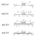
- Figs. from 3 (a) to 3(d) are cross-sectional views illustrating the fabricating steps of a first embodiment according to the present invention, presented in series.
- a single crystalline silicon substrate 1 of p-type, doped with boron (B) of the concentration of 1015/cm3 is prepared.
- a field insulating layer 2 having a window 8 is formed over the surface of the substrate using a conventional method.
- a gate electrode 4 is formed on the surface of the substrate 1 exposed through the window through a gate insulator 3, being surrounded by an insulating film 5 made of silicon dioxide (SiO2).
- the forming methods employed are the known ones.
- a layer portion beneath the exposed surface of the substrate 1 is amorphized by downwardly implanting silicon (Si) ions to the surface of the substrate 1.
- the ions are implanted through the window 8 except for the portion covered by the insulating film 5 under a condition, for example, of an accelerating energy of 40 KeV, and the dose of 4x10¹⁵/cm2.
- An amorphous silicon layer 10 is thus formed beneath the surface of the substrate 1, having a thickness of approximately 300 to 1000 Angstrom.
- the implanting condition is of an accelerating energy of 70 KeV and the dose of 4x10¹⁵/cm2.
- the polysilicon layer 6 is patterned by a conventional photolithographic process such that the doped polysilicon layer 6 is selectively left over the predetermined source and drain regions, namely over the windows 8.
- the substrate 1 is subject to a conventional rapid thermal annealing (RTA) method and heated an 1000 centigrade for 10 seconds.
- RTA rapid thermal annealing
- the implanted phosphorus (P) ions are activated, being diffused from the polysilicon layer 6 into the underlying amorphous silicon layer 10 which is simultaneously recrystallized and converted to a single crystalline silicon layer. Consequently, n-type source and drain regions 17 are formed.
- source and drain regions 17 are shallow diffusion layers with high dopant concentration. The depth of the regions is approximately 600 Angstrom, and the dopant concentration near the interface is approximately 1020/cm3.
- the doped polysilicon layer is formed by ion implanting of the relevant dopant to the polysilicon layer 6.
- the dopant concentration distribution is represented by the diagram D shown in Fig. 1(c).
- the accelerating energy of the dopant ion implantation is selected considering the thickness of the polysilicon layer 6 such that the peak point Pd is located substantially near the interface F.
- the implanted dopant ions go into the amorphized layer 10, being suppressed to proceed further because of the amorphized structure of the layer 10.
- the intrusion of the ions into the underlying single crystalline silicon substrate 1 is thus prevented, and the ions are escaped from the channeling effect.
- the dopant concentration diagram D is rapidly falling down in the amorphized layer 10.
- the diffusion region 17 formed by the subsequent RTA has a reduced depth almost limited within the amorphized layer 10, and the dopant concentration thereof is favorably high since the dopants in the region 17 are supplied from the doped polysilicon layer 6 by thermal diffusion and the dopant ions contained in the polysilicon layer, being added the dopant ions contained in the amorphized layer portion 10.
- the contact resistance between the polysilicon layer 6 and the diffusion layer 17 is substan tially low, since the dopant concentration near the interface between both layers is high.
- the temperature of the associated heat treatment can be favorably low, leading to various fabricating advantages.
- the doped polycristalline layer 6 functions as a contact terminal to each diffusion region 17 since the layer 6 has a favorable electrical conductivity.
- the electrical conductivity can be enhanced by converting the polysilicon layer 6 to a silicide layer, the method of which is disclosed next.
- a field insulating layer 2 having a window 8 is selectively formed over the surface of a silicon substrate 1 of p-type, doped with boron (B) of the concentration of 1015/cm3, employing a conventional method. Then, a gate electrode 4 is formed through a gate insulator 3 on the surface of the substrate exposed through the window 8, being surrounded by an insulating film 6.
- the ions are implanted under the conditions, for example, of a accelerating energy of 40 KeV, and the dose of 4x10¹⁵/cm2.
- the implanting condition is of an accelerating energy of 70 KeV, and the dose of 4x10¹⁵/cm2.
- the polysilicon layer 6 is patterned by a conventional photolithographic process such that the doped polysilicon layer 6 is selectively remained over at least the predetermined source-drain regions, namely diffusion regions. Subsequently, a titanium (Ti) film 11 is formed thereon employing a conventional sputtering method.
- Ti titanium
- a rapid heat treatment using a halogen lamp with a temperature rise of approximately 650 centigrade for 1 minute, the polysilicon layer 6 and the titanium (Ti) film 11 formed thereon, chemically react with each other, forming a titanium silicide layer 12. While the titanium (Ti) film 11 formed over the field insulating oxide layer 2 does not react with each other. The remaining titanium (Ti) film 11 is selectively removed with a usual chemical etching process using acids. After the removal, the substrate is heated at 750 centigrade for 30 seconds.
- RTA rapid heat treatment
- the doped phosphorus (P) ions are diffused from the polysilicon layer 6 into the underlying amorphous silicon layer portion 10, which is simultaneously recrystallized and converted to a single crystalline silicon layer, and the phosphorus (P) ions are activated at the same time.
- n-type source and drain regions 17 having a reduced depth, such as approximately 600 Angstrom, and high dopant concentration of approximately 1020/cm3 almost in the recrystallized layer portion 10.
- the formation of the titanium silicide film 12 and that of the diffused regions (source and drain regions 17) are performed simultaneously.
- a silicide layer is formed first employing a CVD method, and then the phosphorus (P) ions are implanted into the silicide layer to dope the silicide layer. Thereafter, the phosphorous (p) ions are diffused into the amorphous silicon layer 10.
- a platinum silicide layer other than the titanium silicide layer, a platinum silicide layer, a cobalt silicide layer, a tungsten silicide layer, a molybdenum silicide layer, a hafnium silicide layer, a vanadium silicide layer, and a zirconium silicide layer are applicable as a metal silicide layer.
- a dopant material except for phosphorus (P) arsenic (As) is applicable, and as a p-type dopant, boron (B) and boron fluoride (BF2) are applicable.
- the amorphous silicon layer portion is formed by ion planting the surface of the substrate 1. While, an amorphous silicon layer can be formed using a CVD method over the surface of the substrate before or after the formation of the field insulating layer 2. Furthermore, the polysilicon layer 6 may be doped to some degree in advance before the subsequent dopant ion implantation shown in Fig. 3(c) or Fig. 4(c). The preliminary doping of the polysilicon layer 6 is advantageous to reduce doping amount of the following ion implantation.
- the structure of an MOS transistor can be miniaturized and a short channel effect of the transistor is reduced, resulting in substantially improving the function and reliability of the transistor.
- the present invention is further applicable to the improvement of a bipolar transistor by miniaturizing the emitter contact thereof. Furthermore, in the above description, a doped silicon substrate or silicon layers are mentioned. However, it is apparent for the skilled person in the art, that the present invention is applic severelyable to the fabrication of another semiconductor device such as a gallium-arsenic (GaAs) transistor.
- GaAs gallium-arsenic
- the contact resistance and the diffusion resistance of the relevant dopant regions can be reduced and the physical dimensions, particularly the depth of the dopant region is favorably reduced.
- the present invention can effectively contribute to the miniaturization and the improvement of the function of the associated transistor.
Abstract
A method for fabricating a semiconductor device, such as a silicon MOS FET, having diffusion regions with a reduced depth and high dopant concentration, is disclosed. Beneath the surface of the relevant semiconductor substrate, an amorphous layer is formed corresponding to the diffusion regions in advance, following which a doped polysilicon layer is formed. Thereafter, the polysilicon layer is doped employing a dopant ion implantation such that the peak point of the dopant concentration distribution is located substantially near the interface between the silicon substrate and the polysilicon layer. Subsequently, the substrate is subject to a rapid thermal annealing for diffusing the dopant from the doped polysilicon layer, recrystallizing the amorphous layer portion, and activating the dopant contained in the recrystallized layer portion to be the diffusion regions. A silicide layer is used in the place of the polysilicon layer to have a high electrical conductance.
Description
- The present invention relates to a method for forming a semiconductor device, such as a large scale integrated circuit (LSI), having a fine structure suitable for high density integration. Particularly, it relates to a method for forming a shallow and high concentration impurity region in the relevant semiconductor substrate of the device.
- Recently, the miniaturization of a semiconductor device, such as an LSI, is proceeding on, usually based on the well known scaling theory which requires the reduction of the physical dimensions of the device by the scaling factor l/k accompanied with the increase in impurity material (dopant) concentration of the substrate. Consequently, in the art, there has been required the development of an improved fabricating method for forming a shallow diffusion layer with high dopant concentration in order to obtain low diffusion resistance and low contact resistance to the relevant contact terminal.
- Before proceeding further, a brief survey of the ion implanting is described. An accelerated ion entering a solid layer will lose its energy through collision with the nuclei and electrons of the layer, and finally comes to rest. The total distance that the ion travels is referred to as range, and the projection of this distance on the direction of incidence of the ion is referred to as a projected range. The projected range varies depending on the accelerating energy and the collision state with the nuclei and electrons of the implanted layer material. In general, the projected range distribution is theoretically represented by a Gaussian distribution within a single crystalline structure, as shown in an article, titled "Ion implantation in semiconductors - part I" by J. F. Gibbons, published on Proceeding of the IEEE, Vol. 3, March 1968, for example. Experimentally, there is found a projected range distribution of implanted dopant, represented in a peaked concentration distribution curve. Apparently, the distribution of the projected range of implanted dopant is equivalent to that of the concentration of the dopant. Fig. 1 (a) is a schematic diagram A having a peak point Pa at a depth Xa, illustrating the distribution of the dopant concentration with respect to a single crystalline silicon substrate which is implanted with dopant normally incident on the surface of the substrate. The dopant concentration is taken on the coordinate and the depth from the surface is taken on the abscissa. The peak point Pa can be selectively varied by adjusting the associated accelerating energy.
- Regarding the ion implantation, there is an effect known as "the channeling effect". Projected range distribution in a single crystalline body is quite different from those in an amorphous body under the same implantation condition. This is because of the possibility that incident ions can channel along open directions which appear when the incident ion beam is aligned with a low index crystallographic direction. The ions implanted into a single crystalline body are likely to be channeled, proceeding deeper in the body than in the amorphous body. In the diagram A of Fig. 1(a), therefore, the peak point Pa is followed by an elongated tail, which suggests that the direct ion implantation to a single crystalline silicon substrate is not suitable to form a shallow and high dopant concentration diffused region.
- In a method of the prior art, a solid-to-solid thermal diffusion technology is utilized to form a shallow diffusion region in a semiconductor substrate. In the method, a dopant carrying layer is formed over the surface of the substrate corresponding to doped regions (impurity regions) of the relevant MOS FET. The layer, for example, is a polycrystalline silicon layer (hereinafter, referred to as a polysilicon layer) containing dopant therein. The dopant is implanted into the polysilicon layer by employing an ion implanting method. Thereafter, the substrate is subject to a rapid thermal annealing (RTA), resulting in thermal diffusion of dopant contained in the polysilicon layer into the substrate through the interface surface between the polysilicon layer and the substrate.
- Fig. 1 (b) is a schematic diagram, illustrating the distribution of the dopant concentration with respect to the above-described structure composed of the polysilicon layer and the single crystalline silicon substrate which are implanted with dopant. The diagram B represents the dopant concentration distribution when the dopant is implanted with an accelerating energy such that the peak point Pb is located approximately at the mid point Xb of the depth of the polysilicon layer, while the diagram C represents when the dopant is accelerated with higher energy with the result that the peak point pc is shifted to a depth Xc substantially near the interface F. Naturally, the dopant concentration at the interface F of the diagram C is much higher than that of the diagram B. In order to diffuse the dopant into the underlying silicon substrate at a favorably low temperature and form a shallow and high concentration doped region in the substrate, the dopant concentration of the doped polysilicon layer at the interface F is desirably as high as possible. Thus, the peak point of the concentration distribution of the dopant is desirable to be located as close as possible to the interface. Namely, the curve C is more preferable than the curve D. However, the depth X of the peak point P of the distribution is limited because dopant ions once penetrating the polysilicon layer and intruding into the single crystalline silicon substrate, can easily proceed further due to the channneling effect as clearly shown in Fig. 1(b), resulting in forming an undesirably deep dopant region in the substrate. Thus, the reduced depth and the high dopant concentrations are incompatible, providing a problem which must be solved.
- Fig. 2 (a) to (c) illustrate one example of a prior art methods for fabricating a metal-oxide field - effect transistor (MOS FET) having shallow source and drain regions (diffused regions) and contact layers connected to the source and drain regions with low contact resistance. The fabricating steps thereof are briefly described in series with reference to the drawings of Fig. 2(a) to Fig. 2(c).
- Fig. 2(a); A
field insulating layer 2 is selectively formed on asilicon substrate 1 of p-type, doped with boron (B) for example, employing a conventional LOCOS (Local Oxidation of Silicon) method, having awindow 8, through which the surface of thesilicon substrate 1 is exposed. Thewindow 8 is selectively formed corresponding to a diffusion region. Following the formation of thelayer 2, agate electrode 4 is formed on thesilicon substrate 1 through agate insulator 3. Then, thegate electrode 4 is surrounded by aninsulating layer 5. Both of theinsulating layer 5 and thefield insulating layer 2 are made of silicon dioxide (SiO₂). - Fig. 2(b); Subsequently, a
polysilicon layer 6 is formed by a CVD (Chemical Vapor Deposition) method over the entire surface of thesubstrate 1, and phosphorus (P) ions are implanted downwardly to the surface of thesubstrate 1 to dope thepolysilicon layer 6 in the n-type. The ions are distributed within thepolysilicon layer 6. A part of the ions intrude into the upper portion of thesubstrate 1 passing through thepolysilicon layer 6. - Fig. 2(c); Next, the
polysilicon layer 6 is patterned using a photolithographic-process such that thedoped polysilicon layer 6 remains selectively at least over thewindow 8, namely over the predetermined source-drain regions. Thereafter, thesubstrate 1 is subject to a heating process to activate the phosphorus (P) ions, to diffuse the phosphorus (P) ions from thedoped polysilicon layer 6 to thesilicon substrate 1 of p-type with the result that shallow source anddrain regions 7 of n-type are formed in thesubstrate 1 beneath thepolysilicon layer 6. The dopant concentration distribution along the depth direction of thepolysilicon layer 6 and thesubstrate 1 is also represented in Fig. 1(b). A reduced thickness of the doped regions is difficult to be realized due to the channeling effect as described above. - An object of the present invention is to provide a method for fabricating a semiconductor device having physical dimensions of sub-micron order.
- Another object of the present invention is to provide a method for fabricating a dopant diffusion region having a reduced depth, high dopant concentration, and a high diffusion conductance.
- Still another object of the present invention is to provide a method for fabricating an MOS FET having dopant diffusion region with a reduced depth, high dopant concentration, a high diffusion conductance, and a substantially low contact resistance to the associated contact terminal.
- Further object of the present invention is to eliminate the defects of the prior art method that implanted dopant ions tend to proceed deep in a single crystalline semiconductor substrate hindering the realization of a shallow doped region due to the channeling effect.
- To achieve the objects, a method is provided, in which an amorphized silicon layer portion is formed in a single crystalline silicon substrate by implanting ions of silicon or germanium, for example, in a portion beneath the top surface of the substrate, and a polysilicon layer of a doped metal silicide layer, is formed over the amorphized silicon layer portion. The polysilicon layer is doped by ion implantation of dopant. Hereby the dopant ions are suppressed to intrude the underlying single crystalline silicon substrate. Thus the dopant ions escape from the undesirable channeling effect. Thereafter, the substrate is subjected to a rapid thermal annealing. As the result, the dopant contained in the doped polysilicon layer or a doped metal silicide layer is thermally diffused into the amorphous silicon layer and simultaneously the amorphous silicon layer is converted to a single crystalline silicon layer by the heat treatment. Of course, at the same time, the dopants are activated, being not able to diffuse into the substrate passing through the relevant field insulator and gate insulator.
- Since the dopant concentration near the interface between the polysilicon layer and the substrate is kept high, the contact resistance between both layers is substantially low. The dopant ions in the amorphized silicon layer portion are mostly activated therein, and do not go further into the underlying silicon substrate by the heat treatment so that the depth of the diffusion layer is approximately limited within the amorphized layer portion of the substrate. As the result, a shallow and highly concentration dense impurity material layer is formed.
- Furthermore, since the recrystallization of the amorphized silicon layer is easy and the activation ratio of the dopant ions in the amorphized silicon layer is favorably high, the temperature of the associated heat treatment can be selected favorably low, which leads to various fabricating advantages.
- The features and advantages of the present invention will be apparent by reading of the following description and the claims with reference to the following drawings in which like reference numerals represent like parts.
-
- Fig. 1 are schematic diagrams, illustrating the distribution of the dopant concentration taken in the direction normal to the semiconductor substrate,
- Fig. 2 are cross-sectional views illustrating a series of prior art fabricating steps arranged in order,
- Fig. 3 are cross-sectional views, illustrating a series of fabricating steps of a first embodiment according to the present invention arranged in order, and
- Fig. 4 are cross-sectional views illustrating a series of fabricating steps of a second embodiment according to the present invention arranged in order.
- The detail to the present invention is described in the following with reference to drawings.
- Figs. from 3 (a) to 3(d) are cross-sectional views illustrating the fabricating steps of a first embodiment according to the present invention, presented in series.
- Refer to Fig. 3(a); A single
crystalline silicon substrate 1 of p-type, doped with boron (B) of the concentration of 10¹⁵/cm³ is prepared. On thesilicon substrate 1, afield insulating layer 2 having awindow 8 is formed over the surface of the substrate using a conventional method. Then, agate electrode 4 is formed on the surface of thesubstrate 1 exposed through the window through agate insulator 3, being surrounded by an insulatingfilm 5 made of silicon dioxide (SiO₂). The forming methods employed are the known ones. - Refer to Fig. 3(b); Next, a layer portion beneath the exposed surface of the
substrate 1 is amorphized by downwardly implanting silicon (Si) ions to the surface of thesubstrate 1. The ions are implanted through thewindow 8 except for the portion covered by the insulatingfilm 5 under a condition, for example, of an accelerating energy of 40 KeV, and the dose of 4x10¹⁵/cm². Anamorphous silicon layer 10 is thus formed beneath the surface of thesubstrate 1, having a thickness of approximately 300 to 1000 Angstrom. - Refer to Figs. 3(c); Next, a
polysilicon layer 6 with a thickness of approximately 2000 Angstrom, is formed covering the entire surface of thesubstrate 1, employing a conventional CVD method, following which phosphorous (P) ions are implanted into thepolysilicon layer 6 which is doped in the n-type with a dopant concentration of 10²⁰/cm³. The implanting condition is of an accelerating energy of 70 KeV and the dose of 4x10¹⁵/cm². - Refer to Fig. 3(d); Thereafter, the
polysilicon layer 6 is patterned by a conventional photolithographic process such that the dopedpolysilicon layer 6 is selectively left over the predetermined source and drain regions, namely over thewindows 8. - Subsequently, the
substrate 1 is subject to a conventional rapid thermal annealing (RTA) method and heated an 1000 centigrade for 10 seconds. Thereby, the implanted phosphorus (P) ions are activated, being diffused from thepolysilicon layer 6 into the underlyingamorphous silicon layer 10 which is simultaneously recrystallized and converted to a single crystalline silicon layer. Consequently, n-type source and drainregions 17 are formed. Thus formed source and drainregions 17 are shallow diffusion layers with high dopant concentration. The depth of the regions is approximately 600 Angstrom, and the dopant concentration near the interface is approximately 10²⁰/cm³. - In the above described fist embodiment, the doped polysilicon layer is formed by ion implanting of the relevant dopant to the
polysilicon layer 6. The dopant concentration distribution is represented by the diagram D shown in Fig. 1(c). The accelerating energy of the dopant ion implantation is selected considering the thickness of thepolysilicon layer 6 such that the peak point Pd is located substantially near the interface F. Naturally a portion of the implanted dopant ions go into theamorphized layer 10, being suppressed to proceed further because of the amorphized structure of thelayer 10. The intrusion of the ions into the underlying singlecrystalline silicon substrate 1 is thus prevented, and the ions are escaped from the channeling effect. As shown in Fig. 1(c), the dopant concentration diagram D is rapidly falling down in theamorphized layer 10. As the result, thediffusion region 17 formed by the subsequent RTA has a reduced depth almost limited within theamorphized layer 10, and the dopant concentration thereof is favorably high since the dopants in theregion 17 are supplied from the dopedpolysilicon layer 6 by thermal diffusion and the dopant ions contained in the polysilicon layer, being added the dopant ions contained in theamorphized layer portion 10. - In addition, the contact resistance between the
polysilicon layer 6 and thediffusion layer 17 is substan tially low, since the dopant concentration near the interface between both layers is high. - Furthermore, since the recrystallization of the
amorphized silicon layer 10 is easy and the activation ratio of the dopant ions in theamorphized silicon layer 10 is high, the temperature of the associated heat treatment can be favorably low, leading to various fabricating advantages. - The
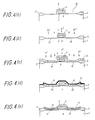
doped polycristalline layer 6 functions as a contact terminal to eachdiffusion region 17 since thelayer 6 has a favorable electrical conductivity. The electrical conductivity can be enhanced by converting thepolysilicon layer 6 to a silicide layer, the method of which is disclosed next. - A second embodiment is described with reference to cross-sectional views of Figs. 4(a) to (e), illustrating the series of the fabricating steps.
- Refer to Fig. 4(a); In the similar manner of the first embodiment, a
field insulating layer 2 having awindow 8 is selectively formed over the surface of asilicon substrate 1 of p-type, doped with boron (B) of the concentration of 10¹⁵/cm³, employing a conventional method. Then, agate electrode 4 is formed through agate insulator 3 on the surface of the substrate exposed through thewindow 8, being surrounded by an insulatingfilm 6. - Refer to Fig. 4(b); Next, an amorphized
silicon layer portion 10 having a depth of approximately 300 to 1000 Angstrom, is formed over an exposed surface of thesubstrate 1 by downwardly implanting silicon (Si) ions thereinto. The ions are implanted under the conditions, for example, of a accelerating energy of 40 KeV, and the dose of 4x10¹⁵/cm². - Refer to Fig. 4(c); Next, a
polysilicon layer 6 having a thickness of approximately 2000 Angstrom, is formed over the entire surface of thesubstrate 1 by a conventional CVD method, following which phosphorous (p) ions are implanted to dope thepolysilicon layer 6 in the n-type to have a dopant concentration of 10²⁰/cm³. The implanting condition is of an accelerating energy of 70 KeV, and the dose of 4x10¹⁵/cm². - Refer to Fig. 4(d); Thereafter, the
polysilicon layer 6 is patterned by a conventional photolithographic process such that the dopedpolysilicon layer 6 is selectively remained over at least the predetermined source-drain regions, namely diffusion regions. Subsequently, a titanium (Ti)film 11 is formed thereon employing a conventional sputtering method. - Refer to Fig. 4(e); Thereafter, upon being subject to a rapid heat treatment (RTA) using a halogen lamp with a temperature rise of approximately 650 centigrade for 1 minute, the
polysilicon layer 6 and the titanium (Ti)film 11 formed thereon, chemically react with each other, forming atitanium silicide layer 12. While the titanium (Ti)film 11 formed over the field insulatingoxide layer 2 does not react with each other. The remaining titanium (Ti)film 11 is selectively removed with a usual chemical etching process using acids. After the removal, the substrate is heated at 750 centigrade for 30 seconds. The doped phosphorus (P) ions are diffused from thepolysilicon layer 6 into the underlying amorphoussilicon layer portion 10, which is simultaneously recrystallized and converted to a single crystalline silicon layer, and the phosphorus (P) ions are activated at the same time. As the result, there are formed n-type source and drainregions 17 having a reduced depth, such as approximately 600 Angstrom, and high dopant concentration of approximately 10²⁰/cm³ almost in the recrystallizedlayer portion 10. - In the above described second embodiment, the formation of the
titanium silicide film 12 and that of the diffused regions (source and drain regions 17) are performed simultaneously. While, in another method, a silicide layer is formed first employing a CVD method, and then the phosphorus (P) ions are implanted into the silicide layer to dope the silicide layer. Thereafter, the phosphorous (p) ions are diffused into theamorphous silicon layer 10. Furthermore, other than the titanium silicide layer, a platinum silicide layer, a cobalt silicide layer, a tungsten silicide layer, a molybdenum silicide layer, a hafnium silicide layer, a vanadium silicide layer, and a zirconium silicide layer are applicable as a metal silicide layer. As a dopant material except for phosphorus (P), arsenic (As) is applicable, and as a p-type dopant, boron (B) and boron fluoride (BF₂) are applicable. - In both of the first and second embodiments, the amorphous silicon layer portion is formed by ion planting the surface of the
substrate 1. While, an amorphous silicon layer can be formed using a CVD method over the surface of the substrate before or after the formation of thefield insulating layer 2. Furthermore, thepolysilicon layer 6 may be doped to some degree in advance before the subsequent dopant ion implantation shown in Fig. 3(c) or Fig. 4(c). The preliminary doping of thepolysilicon layer 6 is advantageous to reduce doping amount of the following ion implantation. - With the above-described fabricating method according to the present invention, the structure of an MOS transistor can be miniaturized and a short channel effect of the transistor is reduced, resulting in substantially improving the function and reliability of the transistor.
- The present invention is further applicable to the improvement of a bipolar transistor by miniaturizing the emitter contact thereof. Furthermore, in the above description, a doped silicon substrate or silicon layers are mentioned. However, it is apparent for the skilled person in the art, that the present invention is applicable to the fabrication of another semiconductor device such as a gallium-arsenic (GaAs) transistor.
- As is apparent from the above description, with respect to the fabrication of a semiconductor device, such as an MOS FET, the contact resistance and the diffusion resistance of the relevant dopant regions can be reduced and the physical dimensions, particularly the depth of the dopant region is favorably reduced. As the result, the present invention can effectively contribute to the miniaturization and the improvement of the function of the associated transistor.
Claims (6)
1. A method for forming diffusion regions in a semiconductor substrate, said method comprising the steps of:
(a) forming an amorphous semiconductor layer portion on a surface of said semiconductor substrate;
(b) forming a semiconductor layer containing dopant material therein over said amorphous semiconductor layer portion;
(c) patterning said semiconductor layer by selectively remaining said semiconductor layer over the predetermined diffusion regions to be formed in said semiconductor substrate; and
(d) heating said semiconductor substrate for thermally diffusing said dopant material contained in said patterned semiconductor layer into said amorphous silicon layer, and simultaneously recrystallizing said amorphous semiconductor layer and activating said dopant material in said recrystallized semiconductor layer, thus forming said diffusion regions in said semiconductor substrate.
2. A method for fabricating diffusion regions in a semiconductor substrate of claim 1, wherein the semiconductor is silicon and said diffusion regions are a source region and a drain region of a metal-insulator-silicon (MIS) field effect transistor (FET).
3. A method for fabricating diffusion regions in a semiconductor substrate of claim 2, wherein said amorphous silicon layer in the step (a) is formed by implanting silicon ions into said silicon substrate.
4. A method for fabricating diffusion regions in a semiconductor substrate of claim 2, wherein the step (c) of forming a silicon layer containing dopant material therein comprises the sub-steps of:
forming a silicon layer over said amorphous silicon layer; and
implanting dopant material into said silicon layer.
forming a silicon layer over said amorphous silicon layer; and
implanting dopant material into said silicon layer.
5. A method for fabricating diffusion regions in a semiconductor substrate, comprising the steps of:
(a) forming an amorphous silicon layer on a surface of said silicon substrate;
(b) forming a silicon layer containing dopant material doped therein over said amorphous silicon layer;
(c) patterning said doped silicon layer to be remained on said amorphous silicon layer;
(d) coating said doped silicon layer with a metal film over said doped silicon layer;
(e) heating said patterned polycrystalline silicon layer,
resulting in chemically reacting said polycrystalline silicon layer and said metal film to form a metal silicide layer with respect to said metal on said polycrystalline layer,
thermally diffusing said dopant material contained in said patterned polycrystalline layer into said amorphous silicon layer, and
simultaneously recrystallizing said amorphous silicon layer, and activating said dopant material in said recrystallized silicon layer, thus forming said diffusion regions.
6. A method for fabricating diffusion regions in a semiconductor substrate of claim 5, wherein said metal is a metal selected from a group of titanium (Ti), tungsten (W), molybdenum (Mo), platinum (Pt), cobalt (Co), hafnium (Hf), vanadium (Va) and zirconium (Zr).
Applications Claiming Priority (2)
| Application Number | Priority Date | Filing Date | Title |
|---|---|---|---|
| JP245569/88 | 1988-09-28 | ||
| JP63245569A JPH0291932A (en) | 1988-09-28 | 1988-09-28 | Manufacture of semiconductor device |
Publications (2)
| Publication Number | Publication Date |
|---|---|
| EP0361078A2 true EP0361078A2 (en) | 1990-04-04 |
| EP0361078A3 EP0361078A3 (en) | 1990-04-25 |
Family
ID=17135668
Family Applications (1)
| Application Number | Title | Priority Date | Filing Date |
|---|---|---|---|
| EP89115513A Withdrawn EP0361078A3 (en) | 1988-09-28 | 1989-08-23 | Method of producing a semiconductor device having shallow highly doped regions |
Country Status (3)
| Country | Link |
|---|---|
| EP (1) | EP0361078A3 (en) |
| JP (1) | JPH0291932A (en) |
| KR (1) | KR920006850B1 (en) |
Cited By (2)
| Publication number | Priority date | Publication date | Assignee | Title |
|---|---|---|---|---|
| WO2007105157A2 (en) * | 2006-03-14 | 2007-09-20 | Nxp B.V. | Source and drain formation |
| US7622343B2 (en) | 1992-10-30 | 2009-11-24 | Semiconductor Energy Laboratory Co., Ltd. | Laser processing method, method for forming a flash memory, insulated gate semiconductor device and method for forming the same |
Families Citing this family (3)
| Publication number | Priority date | Publication date | Assignee | Title |
|---|---|---|---|---|
| JP2833468B2 (en) * | 1994-02-17 | 1998-12-09 | 日本電気株式会社 | Method for manufacturing semiconductor device |
| JP2978736B2 (en) * | 1994-06-21 | 1999-11-15 | 日本電気株式会社 | Method for manufacturing semiconductor device |
| JP5700025B2 (en) * | 2012-11-27 | 2015-04-15 | トヨタ自動車株式会社 | Semiconductor device and manufacturing method thereof |
Citations (2)
| Publication number | Priority date | Publication date | Assignee | Title |
|---|---|---|---|---|
| EP0165547A2 (en) * | 1984-06-21 | 1985-12-27 | International Business Machines Corporation | A method of forming a shallow doped region in a semiconductor substrate |
| EP0227085A2 (en) * | 1985-12-23 | 1987-07-01 | SGS MICROELETTRONICA S.p.A. | A method of manufacturing IGFETs having minimal junction depth using epitaxial recrystallization |
Family Cites Families (4)
| Publication number | Priority date | Publication date | Assignee | Title |
|---|---|---|---|---|
| JPS5853757B2 (en) * | 1976-10-12 | 1983-12-01 | 原子能委員会核能研究所 | Reactor |
| JPS58161344A (en) * | 1982-03-19 | 1983-09-24 | Oki Electric Ind Co Ltd | Manufacture of semiconductor device |
| JPS62130519A (en) * | 1985-12-03 | 1987-06-12 | Sony Corp | Impurity doping to semiconductor thin film |
| JPS62266829A (en) * | 1986-05-14 | 1987-11-19 | Sharp Corp | Formation of shallow junction layer |
-
1988
- 1988-09-28 JP JP63245569A patent/JPH0291932A/en active Pending
-
1989
- 1989-08-23 EP EP89115513A patent/EP0361078A3/en not_active Withdrawn
- 1989-09-27 KR KR1019890013897A patent/KR920006850B1/en not_active IP Right Cessation
Patent Citations (2)
| Publication number | Priority date | Publication date | Assignee | Title |
|---|---|---|---|---|
| EP0165547A2 (en) * | 1984-06-21 | 1985-12-27 | International Business Machines Corporation | A method of forming a shallow doped region in a semiconductor substrate |
| EP0227085A2 (en) * | 1985-12-23 | 1987-07-01 | SGS MICROELETTRONICA S.p.A. | A method of manufacturing IGFETs having minimal junction depth using epitaxial recrystallization |
Non-Patent Citations (2)
| Title |
|---|
| ELECTRONICS LETTERS, vol. 24, no. 15, July 1988, pages 949-950, Stevenage, Herts, GB; K.J. BARLOW: "Formation of submicron PMOS transistors by implantation into silicide" * |
| JAPANESE JOURNAL OF APPLIED PHYSICS. SUPPLEMENTS-17TH CONF. ON SOLID STATE DEVICES AND MATERIALS, Tokyo, 25th-27th August 1985, pages 325-328; N. NATSUAKI et al.: "Refractory-metal-silicide contact formation by rapid thermal annealing" * |
Cited By (3)
| Publication number | Priority date | Publication date | Assignee | Title |
|---|---|---|---|---|
| US7622343B2 (en) | 1992-10-30 | 2009-11-24 | Semiconductor Energy Laboratory Co., Ltd. | Laser processing method, method for forming a flash memory, insulated gate semiconductor device and method for forming the same |
| WO2007105157A2 (en) * | 2006-03-14 | 2007-09-20 | Nxp B.V. | Source and drain formation |
| WO2007105157A3 (en) * | 2006-03-14 | 2007-11-15 | Nxp Bv | Source and drain formation |
Also Published As
| Publication number | Publication date |
|---|---|
| KR920006850B1 (en) | 1992-08-20 |
| EP0361078A3 (en) | 1990-04-25 |
| JPH0291932A (en) | 1990-03-30 |
| KR900005575A (en) | 1990-04-14 |
Similar Documents
| Publication | Publication Date | Title |
|---|---|---|
| US5006476A (en) | Transistor manufacturing process using three-step base doping | |
| JP3211394B2 (en) | Method for manufacturing semiconductor device | |
| US8236675B2 (en) | Semiconductor device and method of fabricating a semiconductor device | |
| US5079182A (en) | Bicmos device having self-aligned well tap and method of fabrication | |
| EP0137645B1 (en) | Method of forming a shallow n-type region | |
| US5536676A (en) | Low temperature formation of silicided shallow junctions by ion implantation into thin silicon films | |
| JPH04226022A (en) | Formation of space in semiconductor struc- tural body | |
| JPS6379368A (en) | Manufacture of high performance bicmos composition with polycrystalline silicon emitter and silicide base | |
| KR100822228B1 (en) | Semiconductor device and method of fabrication | |
| US6130144A (en) | Method for making very shallow junctions in silicon devices | |
| US5593923A (en) | Method of fabricating semiconductor device having refractory metal silicide layer on impurity region using damage implant and single step anneal | |
| JPH04226064A (en) | Interconnection body for semiconductor device use its manufacture | |
| EP0401786B1 (en) | Method of manufacturing a lateral bipolar transistor | |
| US5443994A (en) | Method of fabricating a semiconductor device having a borosilicate glass spacer | |
| US5234847A (en) | Method of fabricating a BiCMOS device having closely spaced contacts | |
| EP0361078A2 (en) | Method of producing a semiconductor device having shallow highly doped regions | |
| EP0325181B1 (en) | A method of manufacturing a polysilicon emitter and a polysilicon gate using the same etch of polysilicon on a thin gate oxide | |
| US5298440A (en) | Method of fabrication of transistor device with increased breakdown voltage | |
| JPH0878674A (en) | Semiconductor device and its manufacture and bipolar transistor | |
| JP2001007325A (en) | Field-effect transistor | |
| JPH05304158A (en) | Semiconductor device and fabrication thereof | |
| JP2000058822A (en) | Manufacture of semiconductor device | |
| JPH1131665A (en) | Manufacture of semiconductor integrated circuit | |
| JP3190370B2 (en) | BiCMOS device having closely spaced contacts and method of manufacturing the same | |
| JP3161379B2 (en) | Semiconductor device and method of manufacturing semiconductor device |
Legal Events
| Date | Code | Title | Description |
|---|---|---|---|
| PUAI | Public reference made under article 153(3) epc to a published international application that has entered the european phase |
Free format text: ORIGINAL CODE: 0009012 |
|
| PUAL | Search report despatched |
Free format text: ORIGINAL CODE: 0009013 |
|
| AK | Designated contracting states |
Kind code of ref document: A2 Designated state(s): DE FR GB |
|
| AK | Designated contracting states |
Kind code of ref document: A3 Designated state(s): DE FR GB |
|
| 17P | Request for examination filed |
Effective date: 19900510 |
|
| 17Q | First examination report despatched |
Effective date: 19921028 |
|
| STAA | Information on the status of an ep patent application or granted ep patent |
Free format text: STATUS: THE APPLICATION HAS BEEN WITHDRAWN |
|
| 18W | Application withdrawn |
Withdrawal date: 19930217 |