EP0359018A2 - Lithographiegerät zur Strukturierung eines Objektes - Google Patents
Lithographiegerät zur Strukturierung eines Objektes Download PDFInfo
- Publication number
- EP0359018A2 EP0359018A2 EP89115843A EP89115843A EP0359018A2 EP 0359018 A2 EP0359018 A2 EP 0359018A2 EP 89115843 A EP89115843 A EP 89115843A EP 89115843 A EP89115843 A EP 89115843A EP 0359018 A2 EP0359018 A2 EP 0359018A2
- Authority
- EP
- European Patent Office
- Prior art keywords
- lithography device
- probes
- electron
- particle
- lithography
- Prior art date
- Legal status (The legal status is an assumption and is not a legal conclusion. Google has not performed a legal analysis and makes no representation as to the accuracy of the status listed.)
- Withdrawn
Links
Images

Classifications
-
- H—ELECTRICITY
- H01—ELECTRIC ELEMENTS
- H01J—ELECTRIC DISCHARGE TUBES OR DISCHARGE LAMPS
- H01J37/00—Discharge tubes with provision for introducing objects or material to be exposed to the discharge, e.g. for the purpose of examination or processing thereof
- H01J37/30—Electron-beam or ion-beam tubes for localised treatment of objects
- H01J37/317—Electron-beam or ion-beam tubes for localised treatment of objects for changing properties of the objects or for applying thin layers thereon, e.g. for ion implantation
- H01J37/3174—Particle-beam lithography, e.g. electron beam lithography
- H01J37/3177—Multi-beam, e.g. fly's eye, comb probe
-
- B—PERFORMING OPERATIONS; TRANSPORTING
- B82—NANOTECHNOLOGY
- B82Y—SPECIFIC USES OR APPLICATIONS OF NANOSTRUCTURES; MEASUREMENT OR ANALYSIS OF NANOSTRUCTURES; MANUFACTURE OR TREATMENT OF NANOSTRUCTURES
- B82Y10/00—Nanotechnology for information processing, storage or transmission, e.g. quantum computing or single electron logic
-
- B—PERFORMING OPERATIONS; TRANSPORTING
- B82—NANOTECHNOLOGY
- B82Y—SPECIFIC USES OR APPLICATIONS OF NANOSTRUCTURES; MEASUREMENT OR ANALYSIS OF NANOSTRUCTURES; MANUFACTURE OR TREATMENT OF NANOSTRUCTURES
- B82Y40/00—Manufacture or treatment of nanostructures
-
- H—ELECTRICITY
- H01—ELECTRIC ELEMENTS
- H01J—ELECTRIC DISCHARGE TUBES OR DISCHARGE LAMPS
- H01J37/00—Discharge tubes with provision for introducing objects or material to be exposed to the discharge, e.g. for the purpose of examination or processing thereof
- H01J37/30—Electron-beam or ion-beam tubes for localised treatment of objects
- H01J37/3002—Details
- H01J37/3007—Electron or ion-optical systems
Definitions
- the invention relates to a lithography device for structuring an object with a plurality of particle probes.
- a lithography device (electron beam writer) is known, the electron-optical column of which has a control panel for generating a plurality of individually deflectable or probable electron probes.
- This aperture which is described in more detail in EP-0 191 439 A1, essentially consists of a silicon wafer, the central part of which is designed as a self-supporting membrane and is provided with a linear arrangement of square recesses. An electrode system arranged in the region of the recesses serves as the deflection unit.
- the electron probes are fed from a common source, so that each of the partial beams only accounts for a fraction of the available source current.
- the probe current should be as high as possible.
- the invention has for its object to provide a lithography device of the type mentioned, in which the probe current is significantly higher than in conventional systems.
- the lithography device should have a high resolution. According to the invention, these objects are achieved by a lithography device according to claim 1.
- the subclaims relate to advantageous developments of the invention.
- the advantage that can be achieved with the invention is in particular that the throughput of structured semiconductor bodies increases significantly.
- 1 to 3 show exemplary embodiments of lithography devices according to the invention.
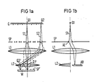
- the lithography device shown schematically in FIG. 1 comprises a beam generator Q consisting of a plurality of electron sources Q1, Q2, a control plate SP for shaping and blanking out the electron probes S1, S2 emanating from the sources Q1, Q2 and electron optics consisting of a condenser lens L1 and an objective lens L2 , which images the square or rectangular recesses of the control plate SP illuminated by the probes S1, S2 on the semiconductor body W coated with a resist.
- the distortion that occurs when imaging electron sources Q1, Q2, which are preferably arranged along a line, is considerably reduced in the lithography device according to the invention by a telecentric beam path.
- the intermediate images Q1 ', Q2' of the source Q1, Q2 are in the objective lens L2.
- the beam cross section of the electron probes S1, S2 then becomes minimal within the objective lens L2, which ensures particularly low aberrations and thus a high resolution.
- the diaphragm known from US-A-4,724,328 or EP-0 191 439 A1 can be used as the control plate SP.
- This preferably consists of a silicon wafer, which is formed in the central region as a self-supporting membrane and is also provided with a linear arrangement of square or rectangular recesses.
- a deflection element AE in particular a pair of capacitor plates, is associated with each of the recesses the electrodes of which apply the signal to deflect the respective electron probe S1.
- the deflected probe S1 strikes the aperture AB, which is preferably arranged inside the objective lens L2, and is thereby blanked out. In this way, any light-dark pattern can be created with the help of the linear special array.
- the lithography device shown schematically in FIG. 2 likewise comprises a beam generator Q with a plurality of electron sources Q1, Q2 arranged along a line, a control plate SP for individually blanking out the electron probes S1, S2 emanating from the sources Q1, Q2 and one consisting of a condenser lens L1 and an objective lens L2 existing telecentric electron optics for focusing the electron probes S1, S2 on the semiconductor body W to be structured.
- an optic consisting of the lenses L3 and L4 is also provided, which images the linear electron source Q telecentrically into the plane of the control plate SP.
- a capacitor element AE is again assigned to each of the recesses in the control plate SP in order to deflect the electron probes S1, S2, if necessary, onto a blanking aperture AB arranged in the beam path below the control plate SP (see FIG. 2b).
- each electron probe S1, S2 is fed from its own source Q1 or Q2.
- electron sources Q1, Q2 come in particular from J. Vac. Sci. Technol. A5 (4), July / August 1987, pages 1544 to 1548 known silicon cold cathodes, laser-pumped photocathodes (Applied Physics Letters 51.2, July 1987, pages 145 to 147), LaB6 single-crystal cutting edge emitter (US-A-4 724 328) and the in SRI International Technical Note 2, November 1984 field emission cathodes. Silicon cold cathodes and field mission cathodes according to Spindt offer special advantages, the emission current of which can be switched very quickly.
- a lithography device equipped with such sources does not require a control plate SP with the associated illumination optics L3, L4, since the blanking of the electron probes S1, S2 is then carried out in the beam generator Q itself.
- the structure of the lithography device is considerably simplified.
Landscapes
- Chemical & Material Sciences (AREA)
- Engineering & Computer Science (AREA)
- Nanotechnology (AREA)
- Analytical Chemistry (AREA)
- Physics & Mathematics (AREA)
- Crystallography & Structural Chemistry (AREA)
- Mathematical Physics (AREA)
- Theoretical Computer Science (AREA)
- Condensed Matter Physics & Semiconductors (AREA)
- General Physics & Mathematics (AREA)
- Manufacturing & Machinery (AREA)
- Electron Beam Exposure (AREA)
Abstract
Description
- Die Erfindung bezieht sich auf ein Lithographiegerät zur Strukturierung eines Objektes mit einer Vielzahl von Teilchensonden.
- Aus der US-A-4 724 382 ist ein Lithographiegerät (Elektronenstrahlschreiber) bekannt, dessen elektronenoptische Säule eine Steuerblende zur Erzeugung einer Vielzahl individuell ablenk- bzw. austastbarer Elektronensonden aufweist. Diese in der EP-0 191 439 A1 näher beschriebene Blende besteht im wesentlichen aus einer Siliziumscheibe, deren mittlerer Teil als freitragende Membran ausgebildet und mit einer linienförmigen Anordnung quadratischer Ausnehmungen versehen ist. Als Ablenkeinheit dient ein im Bereich der Ausnehmungen angeordnetes Elektrodensystem.
- Weitere Lithographiegeräte sind aus den US-A-4 130 761, 4 153 843, 4 409 487 und 4 524 278 bekannt.
- In diesen Lithographiegeräten werden die Elektronensonden aus einer gemeinsamen Quelle gespeist, so daß auf jeden der Teilstrahlen nur ein Bruchteil des verfügbaren Quellenstroms entfällt. Zur Steigerung des Durchsatzes an strukturierten Halbleiterwafern sollte der Sondenstrom aber möglichst hoch sein.
- Der Erfindung liegt die Aufgabe zugrunde, ein Lithographiegerät der eingangs genannten Art anzugeben, in dem der Sondenstrom deutlich höher ist als in konventionellen Systemen. Außerdem soll das Lithographiegerät eine hohe Auflösung besitzen. Diese Aufgaben werden erfindungsgemäß durch ein Lithographiegerät nach Patentanspruch 1 gelöst. Die Unteransprüche betreffen vorteilhafte Weiterbildungen der Erfindung.
- Der mit der Erfindung erzielbare Vorteil besteht insbesondere darin, daß sich der Durchsatz an strukturierten Halbleiterkörpern deutlich erhöht.
- Die Erfindung wird im folgenden anhand der Zeichnungen näher erläutert. Hierbei zeigen die Figuren 1 bis 3 Ausführungsbeispiele erfindungsgemäßer Lithographiegeräte.
- Das in Figur 1 schematisch dargestellte Lithographiegerät umfaßt einen aus mehreren Elektronenquellen Q1, Q2 bestehenden Strahlerzeuger Q, eine Steuerplatte SP zur Formung und Austastung der von den Quellen Q1, Q2 ausgehenden Elektronensonden S1, S2 und eine aus einer Kondensorlinse L1 und einer Objektivlinse L2 bestehende Elektronenoptik, die die von den Sonden S1, S2 ausgeleuchteten quadratischen oder rechteckförmigen Ausnehmungen der Steuerplatte SP verkleinert auf den mit einem Resist beschichteten Halbleiterkörper W abbildet. Die bei der Abbildung der vorzugsweise entlang einer Linie angeordneten Elektronenquellen Q1, Q2 auftretende Verzeichnung wird in dem erfindungsgemäßen Lithographiegerät durch einen telezentrischen Strahlengang erheblich reduziert. Hierbei ist es von Vorteil, wenn die Zwischenbilder Q1′, Q2′ der Quelle Q1, Q2 in der Objektivlinse L2 liegen. Der Strahlquerschnitt der Elektronensonden S1, S2 wird dann innerhalb der Objektivlinse L2 minimal, was besonders geringe Aberrationen und damit eine hohe Auflösung gewährleistet.
- Als Steuerplatte SP kann insbesondere die aus der US-A-4 724 328 bzw. EP-0 191 439 A1 bekannte Blende verwendet werden. Diese besteht dann vorzugsweise aus einer Siliziumscheibe, die im mittleren Bereich als freitragende Membran ausgebildet und mit einer ebenfalls linienförmigen Anordnung quadratischer oder rechteckförmiger Ausnehmungen versehen ist. Wie die Figur 1b in der Seitenansicht zeigt, ist jeder der Ausnehmungen ein Ablenkelement AE, insbesondere ein Kondensatorplattenpaar, zugeordnet, an dessen Elektroden das Signal zur Ablenkung der jeweiligen Elektronensonde S1 anliegt. Die abgelenkte Sonde S1 trifft auf die vorzugsweise innerhalb der Objektivlinse L2 angeordnete Blende AB und wird dadurch ausgetastet. Auf diese Weise lassen sich beliebige hell-dunkel Muster mit Hilfe des linienförmigen Sonderarrays erzeugen.
- Das in Figur 2 schematisch dargestellte Lithographiegerät umfaßt ebenfalls einen Strahlerzeuger Q mit mehreren entlang einer Linie angeordneten Elektronenquellen Q1, Q2, eine Steuerplatte SP zur individuellen Austastung der von den Quellen Q1, Q2 ausgehenden Elektronensonden S1, S2 und eine aus einer Kondensorlinse L1 und einer Objektivlinse L2 bestehende telezentrische Elektronenoptik zur Fokussierung der Elektronensonden S1, S2 auf den zu strukturierenden Halbleiterkörper W. Zusätzlich ist noch eine aus den Linsen L3 und L4 bestehende Optik vorgesehen, die die linienförmige Elektronenquelle Q telezentrisch in die Ebene der Steuerplatte SP abbildet. Im Unterschied zu dem in Figur 1 dargestellten Lithographiegerät, bei dem die Elektronenquelle Q und die Steuerplatte SP als Objekt ebenso wie deren Bilder Q1′, Q2′ bzw. SP′ jeweils räumlich getrennt vorliegen (Köhler-Beleuchtung), ist in diesem Ausführungsbeispiel die sogenannte kritische Beleuchtung verwirklicht, wo Quelle Q1′, Q2′ und Objekt SP ebenso wie deren Bilder Q1˝, Q2˝ bzw. SP′ jeweils zusammenfallen. Jeder der Ausnehmungen der Steuerplatte SP ist wieder ein Kondensatorelement AE zugeordnet, um die Elektronensonden S1, S2 gegebenenfalls auf eine im Strahlengang unterhalb der Steuerplatte SP angeordnete Austastblende AB abzulenken (siehe Figur 2b).
- In den erfindungsgemäßen Lithographiegeräten wird jede Elektronensonde S1, S2 aus einer eigenen Quelle Q1 bzw. Q2 gespeist. Als Elektronenquellen Q1, Q2 kommen insbesondere die aus J. Vac. Sci. Technol. A5 (4), Juli/August 1987, Seite 1544 bis 1548 bekannten Silizium-Kaltkathoden, lasergepumpte Photokathoden (Applied Physics Letters 51.2, Juli 1987, Seite 145 bis 147), LaB6-Einkristall-Schneidenemitter (US-A-4 724 328) und die in SRI International Technical Note 2, November 1984 beschriebenen Feldemissionskathoden in Betracht. Besondere Vorteile bieten Silizium-Kaltkathoden und Feldmissionskathoden nach Spindt, deren Emissionsstrom sich sehr schnell schalten läßt.
- Ein mit solchen Quellen ausgestattetes Lithographiegerät benötigt keine Steuerplatte SP mit der zugehörigen Beleuchtungsoptik L3, L4, da die Austastung der Elektronensonden S1, S2 dann im Strahlerzeuger Q selbst vorgenommen wird. Wie die Figur 3 schematisch zeigt, vereinfacht sich der Aufbau des Lithographiegerätes dadurch erheblich.
Claims (7)
Applications Claiming Priority (2)
| Application Number | Priority Date | Filing Date | Title |
|---|---|---|---|
| DE3831526 | 1988-09-16 | ||
| DE3831526 | 1988-09-16 |
Publications (2)
| Publication Number | Publication Date |
|---|---|
| EP0359018A2 true EP0359018A2 (de) | 1990-03-21 |
| EP0359018A3 EP0359018A3 (de) | 1990-08-22 |
Family
ID=6363096
Family Applications (1)
| Application Number | Title | Priority Date | Filing Date |
|---|---|---|---|
| EP89115843A Withdrawn EP0359018A3 (de) | 1988-09-16 | 1989-08-28 | Lithographiegerät zur Strukturierung eines Objektes |
Country Status (3)
| Country | Link |
|---|---|
| US (1) | US4996441A (de) |
| EP (1) | EP0359018A3 (de) |
| JP (1) | JPH02121251A (de) |
Cited By (20)
| Publication number | Priority date | Publication date | Assignee | Title |
|---|---|---|---|---|
| EP0580318A1 (de) * | 1992-07-14 | 1994-01-26 | AT&T Corp. | Bauelementeherstellung im Submikronbereich unter Verwendung eines Mehrlochblendenfilters |
| US5973332A (en) * | 1996-03-04 | 1999-10-26 | Canon Kabushiki Kaisha | Electron beam exposure method, and device manufacturing method using same |
| EP0955641A1 (de) * | 1998-05-05 | 1999-11-10 | Carl Zeiss | Beleuchtungssystem insbesondere für die EUV-Lithographie |
| US6438199B1 (en) | 1998-05-05 | 2002-08-20 | Carl-Zeiss-Stiftung | Illumination system particularly for microlithography |
| EP1434240A1 (de) * | 1998-05-05 | 2004-06-30 | Carl Zeiss | Beleuchtungssystem insbesondere für die EUV-Lithographie |
| US6858853B2 (en) | 1998-05-05 | 2005-02-22 | Carl Zeiss Smt Ag | Illumination system particularly for microlithography |
| US6859515B2 (en) | 1998-05-05 | 2005-02-22 | Carl-Zeiss-Stiftung Trading | Illumination system, particularly for EUV lithography |
| US6859328B2 (en) | 1998-05-05 | 2005-02-22 | Carl Zeiss Semiconductor | Illumination system particularly for microlithography |
| US6947120B2 (en) | 1998-05-05 | 2005-09-20 | Carl Zeiss Smt Ag | Illumination system particularly for microlithography |
| US6947124B2 (en) | 1998-05-05 | 2005-09-20 | Carl Zeiss Smt Ag | Illumination system particularly for microlithography |
| US7071476B2 (en) | 1998-05-05 | 2006-07-04 | Carl Zeiss Smt Ag | Illumination system with a plurality of light sources |
| US7109497B2 (en) | 1998-05-05 | 2006-09-19 | Carl Zeiss Smt Ag | Illumination system particularly for microlithography |
| US7126137B2 (en) | 1998-05-05 | 2006-10-24 | Carl Zeiss Smt Ag | Illumination system with field mirrors for producing uniform scanning energy |
| US7142285B2 (en) | 1998-05-05 | 2006-11-28 | Carl Zeiss Smt Ag | Illumination system particularly for microlithography |
| US7186983B2 (en) | 1998-05-05 | 2007-03-06 | Carl Zeiss Smt Ag | Illumination system particularly for microlithography |
| US7248667B2 (en) | 1999-05-04 | 2007-07-24 | Carl Zeiss Smt Ag | Illumination system with a grating element |
| US7329886B2 (en) | 1998-05-05 | 2008-02-12 | Carl Zeiss Smt Ag | EUV illumination system having a plurality of light sources for illuminating an optical element |
| US7443948B2 (en) | 1998-05-05 | 2008-10-28 | Carl Zeiss Smt Ag | Illumination system particularly for microlithography |
| USRE41667E1 (en) * | 1998-05-05 | 2010-09-14 | Carl Zeiss Smt Ag | Illumination system particularly for microlithography |
| USRE42065E1 (en) | 1998-05-05 | 2011-01-25 | Carl Zeiss Smt Ag | Illumination system particularly for microlithography |
Families Citing this family (15)
| Publication number | Priority date | Publication date | Assignee | Title |
|---|---|---|---|---|
| JP2559849B2 (ja) * | 1989-05-23 | 1996-12-04 | 三菱電機株式会社 | Icカード |
| US5384463A (en) * | 1991-06-10 | 1995-01-24 | Fujisu Limited | Pattern inspection apparatus and electron beam apparatus |
| US6104035A (en) * | 1997-06-02 | 2000-08-15 | Canon Kabushiki Kaisha | Electron-beam exposure apparatus and method |
| US6014200A (en) * | 1998-02-24 | 2000-01-11 | Nikon Corporation | High throughput electron beam lithography system |
| WO2001039243A1 (en) * | 1999-11-23 | 2001-05-31 | Ion Diagnostics, Inc. | Electron optics for multi-beam electron beam lithography tool |
| US6977375B2 (en) | 2000-02-19 | 2005-12-20 | Multibeam Systems, Inc. | Multi-beam multi-column electron beam inspection system |
| US6787780B2 (en) * | 2000-04-04 | 2004-09-07 | Advantest Corporation | Multi-beam exposure apparatus using a multi-axis electron lens, fabrication method of a semiconductor device |
| US7122795B2 (en) * | 2001-04-18 | 2006-10-17 | Multibeam Systems, Inc. | Detector optics for charged particle beam inspection system |
| US6614035B2 (en) * | 2002-01-30 | 2003-09-02 | International Business Machines Corporation | Multi-beam shaped beam lithography system |
| EP1602121B1 (de) * | 2003-03-10 | 2012-06-27 | Mapper Lithography Ip B.V. | Vorrichtung zur erzeugung einer vielzahl von teilstrahlen |
| ATE441202T1 (de) * | 2004-05-17 | 2009-09-15 | Mapper Lithography Ip Bv | Belichtungssystem mit einem geladenen teilchenstrahl |
| CA2562722C (en) | 2006-09-12 | 2015-11-24 | Sunwell Engineering Company Limited | Method and apparatus for cooling product |
| JP2013165234A (ja) * | 2012-02-13 | 2013-08-22 | Canon Inc | 荷電粒子光学系、荷電粒子線装置、および物品の製造方法 |
| WO2021104991A1 (en) * | 2019-11-28 | 2021-06-03 | Asml Netherlands B.V. | Multi-source charged particle illumination apparatus |
| EP3828916A1 (de) * | 2019-11-28 | 2021-06-02 | ASML Netherlands B.V. | Bestrahlungsapparat mit mehreren quellen geladener teilchen |
Family Cites Families (9)
| Publication number | Priority date | Publication date | Assignee | Title |
|---|---|---|---|---|
| JPS52119178A (en) * | 1976-03-31 | 1977-10-06 | Toshiba Corp | Electron beam exposure device |
| CA1100237A (en) * | 1977-03-23 | 1981-04-28 | Roger F.W. Pease | Multiple electron beam exposure system |
| FR2443085A1 (fr) * | 1978-07-24 | 1980-06-27 | Thomson Csf | Dispositif de microlithographie par bombardement electronique |
| FR2461281A2 (fr) * | 1979-07-06 | 1981-01-30 | Thomson Csf | Dispositif de microlithographie par bombardement electronique |
| NL8200559A (nl) * | 1982-02-15 | 1983-09-01 | Ir Jan Bart Le Poole Prof Dr | Bestralingsinrichting met bundelsplitsing. |
| US4405487A (en) * | 1982-04-29 | 1983-09-20 | Harrah Larry A | Combination moisture and hydrogen getter |
| DE3504705A1 (de) * | 1985-02-12 | 1986-08-14 | Siemens AG, 1000 Berlin und 8000 München | Aperturblende mit zellenfoermiger mehrlochstruktur und austastelektroden zur erzeugung einer mehrzahl von individuell austastbaren korpuskularstrahlsonden fuer ein lithografiegeraet |
| DE3504714A1 (de) * | 1985-02-12 | 1986-08-14 | Siemens AG, 1000 Berlin und 8000 München | Lithografiegeraet zur erzeugung von mikrostrukturen |
| US4847552A (en) * | 1987-07-07 | 1989-07-11 | The Boeing Company | Detection of electrically conductive materials beneath surface coatings employing eddy currents |
-
1989
- 1989-08-21 US US07/395,976 patent/US4996441A/en not_active Expired - Fee Related
- 1989-08-28 EP EP89115843A patent/EP0359018A3/de not_active Withdrawn
- 1989-09-11 JP JP1235493A patent/JPH02121251A/ja active Pending
Cited By (30)
| Publication number | Priority date | Publication date | Assignee | Title |
|---|---|---|---|---|
| EP0580318A1 (de) * | 1992-07-14 | 1994-01-26 | AT&T Corp. | Bauelementeherstellung im Submikronbereich unter Verwendung eines Mehrlochblendenfilters |
| EP1369895A2 (de) | 1996-03-04 | 2003-12-10 | Canon Kabushiki Kaisha | Elektronenstrahl Belichtungsgerät und Herstellungsverfahren und -vorrichtung |
| US5973332A (en) * | 1996-03-04 | 1999-10-26 | Canon Kabushiki Kaisha | Electron beam exposure method, and device manufacturing method using same |
| EP0794552A3 (de) * | 1996-03-04 | 1999-12-15 | Canon Kabushiki Kaisha | Elektronenstrahl-Belichtungsgerät, Belichtungsverfahren und Verfahren zur Erzeugung eines Objekts |
| US6166387A (en) * | 1996-03-04 | 2000-12-26 | Canon Kabushiki Kaisha | Electron beam exposure apparatus and method |
| EP1369895A3 (de) * | 1996-03-04 | 2004-12-22 | Canon Kabushiki Kaisha | Elektronenstrahl Belichtungsgerät und Herstellungsverfahren und -vorrichtung |
| US6323499B1 (en) | 1996-03-04 | 2001-11-27 | Canon Kabushiki Kaisha | Electron beam exposure apparatus and method, and device manufacturing method |
| US6947120B2 (en) | 1998-05-05 | 2005-09-20 | Carl Zeiss Smt Ag | Illumination system particularly for microlithography |
| US7126137B2 (en) | 1998-05-05 | 2006-10-24 | Carl Zeiss Smt Ag | Illumination system with field mirrors for producing uniform scanning energy |
| EP1434240A1 (de) * | 1998-05-05 | 2004-06-30 | Carl Zeiss | Beleuchtungssystem insbesondere für die EUV-Lithographie |
| US6198793B1 (en) | 1998-05-05 | 2001-03-06 | Carl-Zeiss-Stiftung Trading As Carl Zeiss | Illumination system particularly for EUV lithography |
| US6858853B2 (en) | 1998-05-05 | 2005-02-22 | Carl Zeiss Smt Ag | Illumination system particularly for microlithography |
| US6859515B2 (en) | 1998-05-05 | 2005-02-22 | Carl-Zeiss-Stiftung Trading | Illumination system, particularly for EUV lithography |
| US6859328B2 (en) | 1998-05-05 | 2005-02-22 | Carl Zeiss Semiconductor | Illumination system particularly for microlithography |
| EP0955641A1 (de) * | 1998-05-05 | 1999-11-10 | Carl Zeiss | Beleuchtungssystem insbesondere für die EUV-Lithographie |
| US6947124B2 (en) | 1998-05-05 | 2005-09-20 | Carl Zeiss Smt Ag | Illumination system particularly for microlithography |
| US7071476B2 (en) | 1998-05-05 | 2006-07-04 | Carl Zeiss Smt Ag | Illumination system with a plurality of light sources |
| US7109497B2 (en) | 1998-05-05 | 2006-09-19 | Carl Zeiss Smt Ag | Illumination system particularly for microlithography |
| US6438199B1 (en) | 1998-05-05 | 2002-08-20 | Carl-Zeiss-Stiftung | Illumination system particularly for microlithography |
| US7142285B2 (en) | 1998-05-05 | 2006-11-28 | Carl Zeiss Smt Ag | Illumination system particularly for microlithography |
| US7186983B2 (en) | 1998-05-05 | 2007-03-06 | Carl Zeiss Smt Ag | Illumination system particularly for microlithography |
| US7977651B2 (en) | 1998-05-05 | 2011-07-12 | Carl Zeiss Smt Gmbh | Illumination system particularly for microlithography |
| US7329886B2 (en) | 1998-05-05 | 2008-02-12 | Carl Zeiss Smt Ag | EUV illumination system having a plurality of light sources for illuminating an optical element |
| US7348565B2 (en) | 1998-05-05 | 2008-03-25 | Carl Zeiss Smt Ag | Illumination system particularly for microlithography |
| US7443948B2 (en) | 1998-05-05 | 2008-10-28 | Carl Zeiss Smt Ag | Illumination system particularly for microlithography |
| US7456408B2 (en) | 1998-05-05 | 2008-11-25 | Carl Zeiss Smt Ag | Illumination system particularly for microlithography |
| US7592598B2 (en) | 1998-05-05 | 2009-09-22 | Carl Zeiss Smt Ag | Illumination system particularly for microlithography |
| USRE41667E1 (en) * | 1998-05-05 | 2010-09-14 | Carl Zeiss Smt Ag | Illumination system particularly for microlithography |
| USRE42065E1 (en) | 1998-05-05 | 2011-01-25 | Carl Zeiss Smt Ag | Illumination system particularly for microlithography |
| US7248667B2 (en) | 1999-05-04 | 2007-07-24 | Carl Zeiss Smt Ag | Illumination system with a grating element |
Also Published As
| Publication number | Publication date |
|---|---|
| US4996441A (en) | 1991-02-26 |
| JPH02121251A (ja) | 1990-05-09 |
| EP0359018A3 (de) | 1990-08-22 |
Similar Documents
| Publication | Publication Date | Title |
|---|---|---|
| EP0359018A2 (de) | Lithographiegerät zur Strukturierung eines Objektes | |
| DE102018007652B4 (de) | Teilchenstrahl-System sowie Verfahren zur Stromregulierung von Einzel-Teilchenstrahlen | |
| EP0281743B1 (de) | Detektorobjectiv für Rastermikroskope | |
| DE69432098T2 (de) | Elektronenstrahl-Lithographie-System | |
| EP2197014B1 (de) | Anordnung zur Beleuchtung eines Substrats mit mehreren individuell geformten Partikelstrahlen zur hochauflösenden Lithographie von Strukturmustern | |
| DE102014008083B4 (de) | Teilchenstrahlsystem | |
| EP1280184B1 (de) | Untersuchungssystem zum teilchenoptischen Abbilden eines Objekts, Ablenkvorrichtung für geladene Teilchen sowie Verfahren zum Betrieb derselben | |
| DE2832582C2 (de) | Magnetische Elektronenlinsenanordnung | |
| EP0352552B1 (de) | Verfahren zum Beleuchten eines Objektes in einem Transmissions-Elektronenmikroskop und dazu geeignetes Elektronenmikroskop | |
| DE2702445C3 (de) | Korpuskularstrahloptisches Gerät zur verkleinernden Abbildung einer Maske auf ein zu bestrahlendes Präparat | |
| EP1172837B1 (de) | Verfahren zur Elektronenstrahl-Lithographie und elektronen-optisches Lithographiesystem | |
| EP1389794B1 (de) | Strahlführungssystem, Abbildungsverfahren und Elektronenmikroskopiesystem | |
| DE102020123567A1 (de) | Vielzahl-Teilchenstrahl-System mit Kontrast-Korrektur-Linsen-System | |
| EP0603555B1 (de) | Verfahren zur Beleuchtung mit einem fokussierten Elektronenstrahl und zugehöriges elektronen-optisches Beleuchtungssystem | |
| DE3933317A1 (de) | Saeule zur erzeugung eines fokussierten ionenstrahls | |
| DE102023120127A1 (de) | Teilchenoptische Anordnung, insbesondere Vielstrahl-Teilchenmikroskop, mit einer Magnetanordnung zum Separieren eines primären und eines sekundären teilchenoptischen Strahlenganges mit verbesserter Performance | |
| DE69605053T2 (de) | Kanonenlinse zur Partikelstrahlerzeugung | |
| DE69628367T2 (de) | Rasterelektronenmikroskop | |
| EP1216483B1 (de) | Elektronenoptische linsenanordnung mit verschiebbarer achse | |
| DE102023119451B4 (de) | Vielstrahl-Teilchenstrahlsystem mit elektrostatischer Boosterlinse, Verfahren zum Betreiben eines Vielstrahl-Teilchenstrahlsystems und zugehöriges Computerprogrammprodukt | |
| CH631574A5 (en) | Electron beam device for pattern projection | |
| DE112018007212B4 (de) | Ladungsträgerstrahl-Vorrichtung | |
| EP0360035A2 (de) | Elektronenstrahlerzeuger | |
| DE102004019835B4 (de) | Beleuchtungskondensor für ein Partikeloptik-Projektionssystem | |
| DE2043749A1 (de) | Raster Korpuskularstrahlmikroskop |
Legal Events
| Date | Code | Title | Description |
|---|---|---|---|
| PUAI | Public reference made under article 153(3) epc to a published international application that has entered the european phase |
Free format text: ORIGINAL CODE: 0009012 |
|
| AK | Designated contracting states |
Kind code of ref document: A2 Designated state(s): DE FR GB NL |
|
| PUAL | Search report despatched |
Free format text: ORIGINAL CODE: 0009013 |
|
| AK | Designated contracting states |
Kind code of ref document: A3 Designated state(s): DE FR GB NL |
|
| 17P | Request for examination filed |
Effective date: 19901220 |
|
| 17Q | First examination report despatched |
Effective date: 19930628 |
|
| STAA | Information on the status of an ep patent application or granted ep patent |
Free format text: STATUS: THE APPLICATION IS DEEMED TO BE WITHDRAWN |
|
| 18D | Application deemed to be withdrawn |
Effective date: 19931109 |